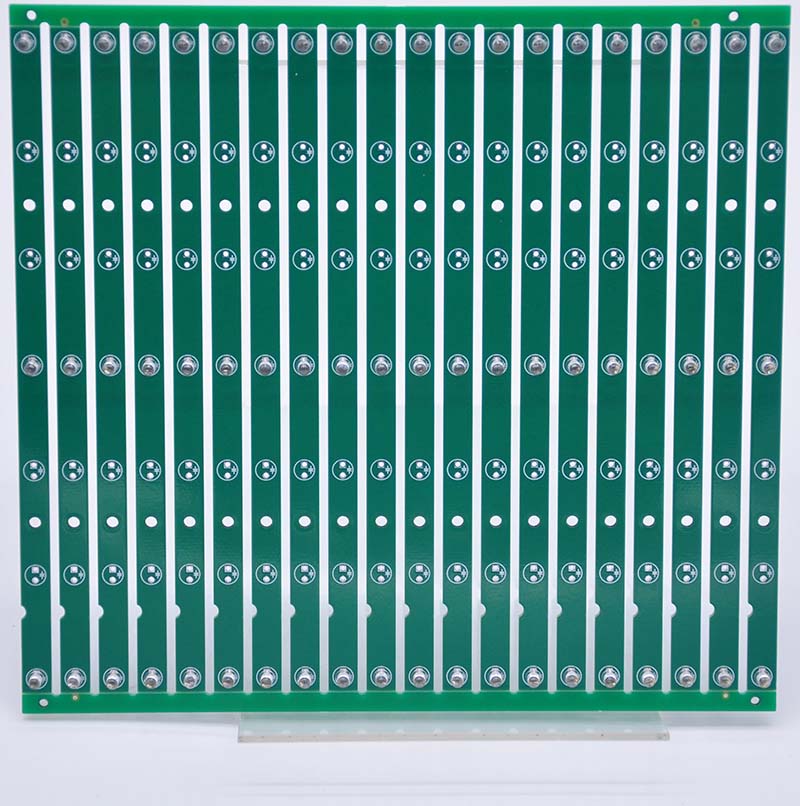
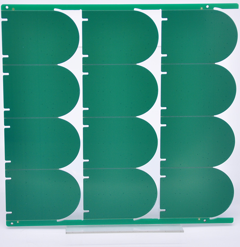
PCB panel sizes are not governed by one universal standard. An 18 × 24 in fabrication panel is a common reference, while an SMT assembly panel is usually smaller and must fit every machine in the line. The right size depends on usable area, board dimensions, rails, spacing, depaneling, rigidity, and equipment limits.
This distinction matters because the sheet purchased by a fabricator, the area available for nesting boards, and the panel delivered to an assembly line are not necessarily the same size. A panel that looks efficient in CAD can still fail at the stencil printer, sag in reflow, or leave insufficient clearance for depaneling. Use the following framework to compare common PCB panel sizes before approving the array.

What Are the Most Common PCB Panel Sizes?
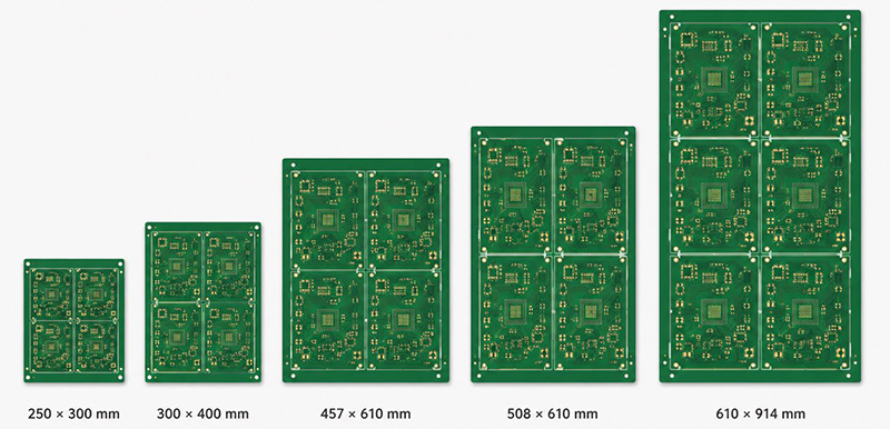
There is no single standard PCB panel size used by every fabricator and assembler. The PCB panel sizes below are practical references seen in fabrication and assembly planning. They are starting points—not guaranteed machine limits or a substitute for supplier confirmation.
| Panel reference | Approximate inches | Typical planning role | Important limitation |
| 250 × 250 mm | 9.84 × 9.84 in | Compact assembly array or smaller fabrication format | Usable area is smaller after rails and process margins |
| 250 × 300 mm | 9.84 × 11.81 in | Compact SMT panel reference | Must fit the narrowest machine and conveyor setting |
| 300 × 400 mm | 11.81 × 15.75 in | Medium assembly or fabrication reference | Rigidity depends on thickness, cutouts, copper, and support |
| 400 × 500 mm | 15.75 × 19.69 in | Larger-format planning reference | May be too large for some SMT lines or fixtures |
| 457 × 610 mm | 18 × 24 in | Widely referenced fabrication panel | Full sheet dimensions do not equal usable nesting area |
| 508 × 610 mm | 20 × 24 in | Alternative fabrication format | Availability and processing rules vary by supplier |
| 610 × 914 mm | 24 × 36 in | Large raw-material or fabrication reference | Usually subdivided before assembly handling |
The best reference size is the one that creates a manufacturable array with acceptable yield, stable handling, and a clean depaneling path. Ask whether a quoted dimension describes raw laminate, a fabrication working panel, or the finished delivery array.
Fabrication Panel vs Usable Area vs SMT Assembly Panel
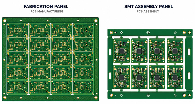
PCB panel sizes can describe four different objects. Confusing them is one of the most common causes of incorrect yield estimates.
| Panel term | Purpose | Main constraint | What to confirm |
| Raw or full fabrication panel | Starting laminate or working sheet | Fabrication equipment and material format | Whether quoted dimensions are raw or process-ready |
| Usable fabrication area | Area available for boards and required features | Process margins, coupons, tooling, and routing space | Confirmed usable width and height |
| Customer array or delivery panel | Multiple boards shipped together | Array count, rails, depaneling, packing, and handling | Overall dimensions and delivery condition |
| SMT assembly panel | Carrier through printing, placement, reflow, AOI, and test | The narrowest handling window across the line | Minimum, maximum, thickness, rail, and support requirements |
A fabricator may optimize several customer arrays within one working panel, but the assembler only handles the delivery panel. This is why PCB fabrication panel size and PCB assembly panel size should be checked separately.
Full PCB Panel Size vs Usable Panel Area
When comparing PCB panel sizes, usable panel area is the full panel area minus process margins and reserved zones. A simple first-pass model is:
Usable width = full width − left margin − right margin
Usable height = full height − top margin − bottom margin
Margins may contain tooling holes, global fiducials, impedance coupons, plating thieving, test structures, barcodes, or gripping zones. Router paths and breakaway rails also consume space. Therefore, an 18 × 24 PCB panel does not provide a universal 18 × 24 in usable area.
For example, if an 18 × 24 in working panel requires a 0.5 in reserved zone on each side, the simplified usable rectangle becomes 17 × 23 in. This is only a calculation example; actual process margins must come from the fabricator. Complex routing, coupons, or process constraints may reduce the usable region further.
How to Calculate PCB Panel Size and Boards per Panel
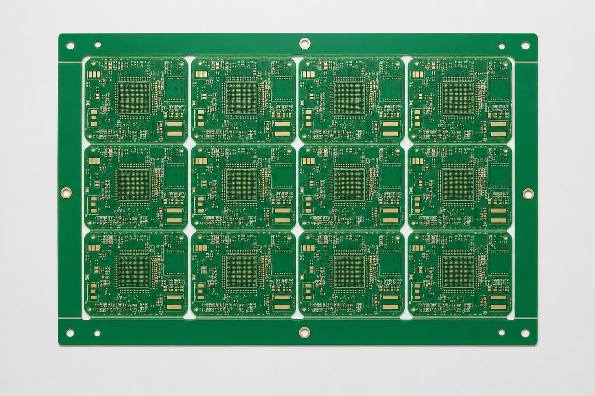
Calculate both board orientations before choosing among PCB panel sizes. Let the usable panel dimensions be Uw and Uh, board dimensions be Bw and Bh, and the required gap between boards be G.
Columns = floor((Uw + G) ÷ (Bw + G))
Rows = floor((Uh + G) ÷ (Bh + G))
Boards per panel = columns × rows
Worked example. Assume a 300 × 400 mm delivery panel with 10 mm rails on all four sides. The simplified usable area is 280 × 380 mm. The single board is 70 × 95 mm, and the selected routing strategy requires a 2 mm gap.
- At 0°: floor((280 + 2) ÷ (70 + 2)) = 3 columns; floor((380 + 2) ÷ (95 + 2)) = 3 rows; total = 9 boards.
- At 90°: floor((280 + 2) ÷ (95 + 2)) = 2 columns; floor((380 + 2) ÷ (70 + 2)) = 5 rows; total = 10 boards.
- Board-area utilization for the 2 × 5 option is (10 × 70 × 95) ÷ (300 × 400) = 55.4% of the full delivery-panel area.
The rotated layout fits one more board, but quantity is not the only approval criterion. The 2 × 5 array must still pass checks for rail direction, conveyor support, component orientation, copper balance, tooling access, and depaneling stress. If it becomes long and flexible, the 3 × 3 option may be safer despite its lower count.
Minimum and Maximum PCB Panel Size Across the SMT Line
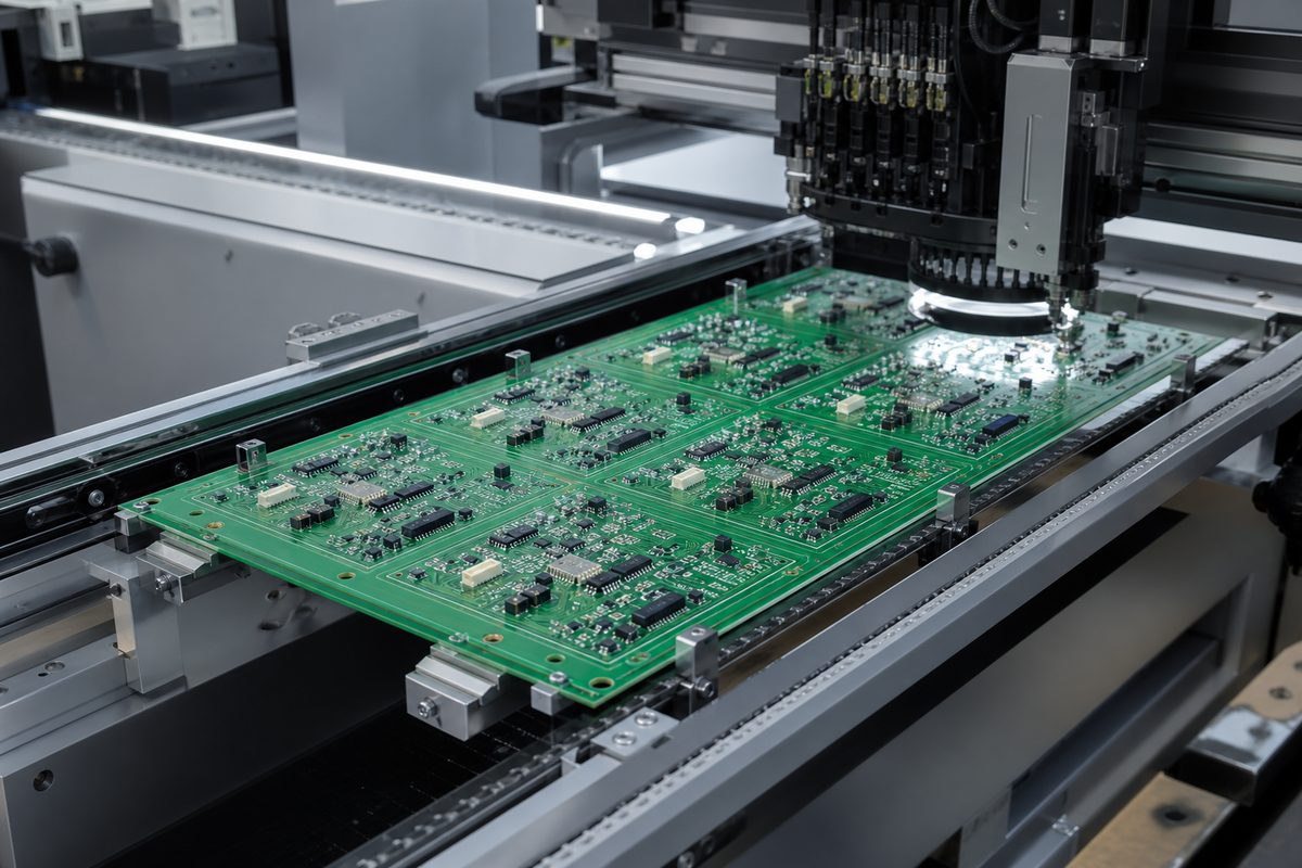
The minimum and maximum PCB panel sizes for assembly are set by the complete line, not by one machine in isolation. Check the stencil printer, loader, conveyor, pick-and-place machine, reflow oven, AOI, ICT or FCT fixture, depaneling equipment, and any manual carriers. The smallest maximum—or the largest minimum—becomes the controlling limit.
- Too small: the board may not clamp, convey, or expose enough edge area for fiducials and tooling.
- Too large: the panel may exceed a transport window, fixture, stencil format, or safe manual-handling range.
- Too flexible: a nominally acceptable panel may sag during printing, placement, or reflow.
- Too heavy: dense components or metal structures may overload support assumptions.
BestPCBS separates standard-process dimensions from special-process review in its controlled PCB Manufacturing Capability data. The following values describe confirmed finished-board and V-cut capabilities; they are not universal industry standards and do not replace a project-specific panel review.
| Confirmed capability item | Standard process | Special process or review condition |
| Finished board maximum dimension | Within 600 mm | Single/double-sided FR-4: 600–1980 mm; multilayer FR-4: 600–750 mm |
| Finished board minimum dimension | 5 mm | A single side of 5–10 mm is shipped by panel |
| Minimum distance between two V-cut lines | 8 mm | Array interaction requires engineering confirmation |
| V-cut board thickness range | 0.6–3.5 mm | More than 4 mm requires a special process |
| Minimum trace-to-board-edge distance for V-cut or routing | 8 mil | Component and mechanical clearances still require DFM review |
A PCB can be fabricable yet unsuitable for an SMT line, so the finished delivery panel must be approved against assembly equipment as well as fabrication capability.
How Rails, Board Spacing, Tooling Holes, and Fiducials Change Panel Dimensions
Every handling feature uses panel area. Add these features before calculating final yield, not after the array count has been fixed.
| Design element | Why it is used | Effect on dimensions | Who confirms it |
| Edge rails | Conveyor support, clamping, fiducials, and edge clearance | Increase overall width, height, or both | Assembler with fabricator review |
| Board spacing | Allows scoring, routing, tabs, and safe separation | Accumulates between every row and column | Fabricator based on depaneling method |
| Tooling holes | Locates the panel in fixtures and processes | Requires reserved rail or margin area | Assembler and fixture owner |
| Global fiducials | Aligns the complete panel for printing and placement | Requires clear optical zones, usually on rails | Assembler |
| Local fiducials | Improves alignment for fine-pitch devices or individual boards | Uses board-level surface area | PCB and assembly engineers |
| Coupons and labels | Supports process control, traceability, or testing | Consumes fabrication or rail space | Fabricator and quality team |
A complete panel drawing should identify the overall dimensions, board array, rails, board spacing, score or router path, tabs, tooling holes, fiducials, orientation, coupon area, barcode zone, and bad-board marking method. Do not assume one tooling-hole or rail dimension works for every production line.
V-Score vs Tab Routing: How the Method Changes Panel Size
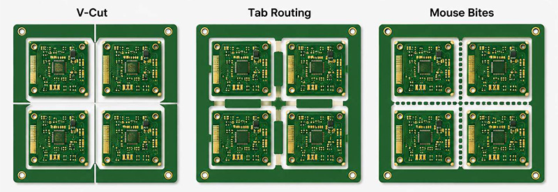
V-scoring suits straight, continuous separation lines and regular rectangular arrays. Tab routing supports irregular outlines and selective separation, but it needs router clearance, tabs, and often mouse-bite finishing. The method changes both the required spacing and the residual stress at the board edge.
| Decision factor | V-score | Tab routing |
| Board outline | Best for straight shared edges | Works with curves and irregular shapes |
| Spacing | Can support closely arranged straight edges, subject to process rules | Needs a router path plus tab locations |
| Edge result | Leaves a scored separation edge | May leave tab or mouse-bite witness marks |
| Component risk | Board bending during separation can stress nearby parts | Tab cutting can reduce bending but needs tool clearance |
| Panel rigidity | Long score lines can weaken the array | Tab number and placement control stiffness |
Minimum and maximum V-cut panel size are supplier- and equipment-specific. Confirm V-cut line spacing, board thickness, component clearance, scoring direction, and permitted edge condition before finalizing the panel.
How Board Thickness, Weight, and Copper Balance Affect Panel Stability
A larger panel is not automatically more economical. Thin laminates, long unsupported spans, large cutouts, asymmetric copper, heavy components, and too few connecting tabs can produce sag or twist. That movement can affect solder-paste release, placement height, reflow support, AOI focus, and depaneling.
Request engineering review when the panel combines two or more risk factors: a long aspect ratio, thin construction, dense copper on one side, heavy connectors, large routed openings, components close to break lines, or narrow rails. Possible responses include changing orientation, reducing the array, widening rails, adding temporary support, balancing copper, repositioning tabs, or using a carrier.
How PCB Panel Size Affects Material Utilization and Cost
The economics of PCB panel sizes include more than laminate area. Cost can be affected by the number of boards per working panel, routing time, wasted edge strips, rail area, tooling, stencil and fixture compatibility, assembly handling, test access, depaneling labor, and the risk of damaging multiple boards at once.
A high-count array may look attractive but lose its advantage if it needs a custom carrier, slows handling, or increases breakaway damage. Compare at least two orientations and, where practical, two delivery-panel sizes. For a realistic quotation, pair the proposed layout with the quantity and process data described in a custom PCB cost guide.
The useful target is not maximum geometric utilization. It is the lowest stable cost per acceptable board after fabrication, assembly, test, and depaneling constraints are included.
How to Choose the Right PCB Panel Size
- Confirm the exact single-board outline, thickness, stack-up, copper weight, and edge-mounted components.
- Ask the fabricator for its working-panel formats, confirmed usable area, process margins, and relevant special-process limits.
- Ask the assembler for the minimum and maximum handling dimensions of every machine and fixture in the line.
- Select V-score, tab routing, or another approved separation method based on outline, edge quality, and component stress.
- Add rails, board gaps, fiducials, tooling holes, coupons, and traceability zones.
- Calculate both 0° and 90° layouts, including the spacing between every row and column.
- Review stiffness, copper balance, component weight, conveyor support, and depaneling forces.
- Approve one controlled panel drawing with the fabricator and the provider of custom PCB assembly services.
Early joint review prevents the common handoff problem in which a fabrication-efficient panel has to be rebuilt for SMT. It also gives both suppliers one agreed definition of the overall panel dimensions and usable area.
What Information Should You Send for PCB Panel Review?
Send enough information for the fabricator and assembler to evaluate the same panel—not separate assumptions.
- Gerber, ODB++, IPC-2581, or another reviewable PCB data package
- Board outline, single-board dimensions, thickness, stack-up, and copper weight
- Required board quantity per delivery panel, or permission to optimize the array
- Assembly side, component overhang, edge clearance, and process flow
- V-score or tab-route preference and the required finished edge
- Rail, fiducial, tooling-hole, barcode, coupon, and bad-board marking requirements
- Delivery condition: individual boards, bare-board panels, or assembled panels
- Order quantity, test method, fixture constraints, and depaneling responsibility
If no customer array is mandatory, submit the single-board production files and ask the fabricator to propose a panel for joint DFM approval. That approach is often safer than locking dimensions before the SMT line and separation method are known.
FAQs About PCB Panel Sizes
Q1. Is there one universal standard PCB panel size?
A1. No—there is no universal panel size. Common dimensions are planning references. Each fabricator and assembler has its own material formats, process margins, equipment windows, and preferred arrays. Confirm whether a stated size means a raw sheet, usable fabrication area, or delivery panel.
Q2. How many PCBs fit on an 18 × 24 inch panel?
A2. The count depends on usable area and layout rules. Subtract fabrication margins, rails, coupons, router paths, and required spacing, then calculate both board orientations. Board outline, depaneling method, and process support can make the highest geometric count unsuitable.
Q3. Do panel rails count toward the overall PCB panel dimensions?
A3. Yes—rails are normally included in the delivered panel dimensions. They consume space but provide conveyor support, clamping area, tooling locations, and global fiducials. State both the overall panel size and the internal array size on the drawing.
Q4. What is the minimum PCB panel size for SMT assembly?
A4. The assembly line determines the practical minimum. A small board may need rails or a multi-board array so the printer, conveyor, placement machine, reflow oven, and inspection equipment can grip and transport it reliably.
Q5. What is the maximum V-cut PCB panel size?
A5. There is no universal maximum V-cut size. The limit depends on the supplier’s scoring equipment, material, thickness, score direction, panel rigidity, and downstream assembly line. Obtain a project-specific confirmation instead of applying another supplier’s published number.
Q6. Should I panelize the PCB myself or let the manufacturer do it?
A6. Let the manufacturer optimize it unless your assembly line requires a controlled array. If you provide the panel, have both fabrication and assembly teams review it. Never assume a CAD array is production-ready without checking tooling and depaneling.
Q7. When should small or prototype PCBs be panelized?
A7. Panelize when individual handling is unreliable or inefficient. Very small boards often need rails or an array for solder-paste printing, placement, reflow, inspection, or test. For low quantities, balance easier handling against panel setup and depaneling work.
Q8. Can different PCB designs share one panel?
A8. Mixed-design panels are possible only with supplier approval. Different outlines, copper distribution, layer constructions, quantities, and test requirements can complicate fabrication and assembly. Confirm fabrication rules, traceability, bad-board handling, and order acceptance before nesting different designs.
Q9. Does rotating boards reduce PCB panel cost?
A9. Rotation can improve yield, but it does not always reduce total cost. A rotated layout may fit more boards yet create poor conveyor support, unfavorable grain or copper behavior, awkward component orientation, or greater depaneling risk. Compare the complete process.
Q10. What panel files should be approved before production?
A10. Approve one dimensioned panel drawing and its production data. The package should show the array, overall size, rails, gaps, score or router paths, tabs, fiducials, tooling holes, orientation, labels, coupons, and bad-board marking requirements.
Conclusion
PCB panel sizes should be chosen by working backward from usable fabrication area, assembly-line handling, depaneling, and mechanical stability. Common PCB panel sizes provide a useful starting point, but the approved panel must reflect the actual board, process, and supplier limits. Calculate both orientations, include every rail and gap, and have fabrication and assembly review the same controlled drawing.
Send your Gerber files, board outline, assembly side, quantity, and preferred delivery format to sales@bestpcbs.com for a DFM panel review.