PCB manufacturing PCB manufacturing
Home > Blog

2 layer PCB

Practical 2 Layer PCB Stackup Guide for Manufacturing
Thursday, August 6th, 2026

An 2 layer PCB stackup looks simple, but it still affects board thickness, copper weight, routing space, grounding, impedance expectations, assembly yield, and final product fit. For engineers and buyers, the practical question is not only whether a board has two copper layers. It is whether the finished PCB can match the drawing, connector, enclosure, soldering process, and test requirement without avoidable rework.

EBest Circuit (Best Technology) supports 2 layer FR4 PCB fabrication, stackup review, copper thickness confirmation, surface finish selection, SMT assembly, inspection, testing coordination, and small-batch production. If your project already has Gerber files, ODB++, stackup notes, BOM, CPL, drawings, or assembly requirements, please send them to sales@bestpcbs.com for engineering review before production.
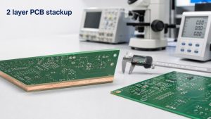
2 layer PCB stackup
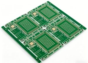
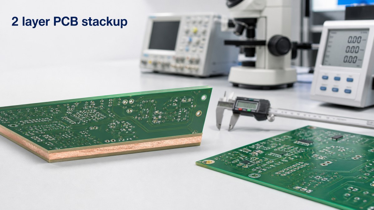
A 2 layer PCB stackup should be reviewed together with board thickness, copper weight, routing, and assembly needs.

What Is a 2 Layer PCB Stackup?

A 2 layer PCB stackup is the layer structure of a printed circuit board with one copper layer on the top side and one copper layer on the bottom side. Between the copper layers, the board normally uses an insulating core material such as FR4. Solder mask, silkscreen, and surface finish are then added according to the production requirement.

In everyday quoting, buyers may also call this a double sided PCB, two layer PCB, or 2 layer circuit board. These terms are closely related, but the stackup is the part that tells the manufacturer how the board thickness, copper, dielectric material, and layer arrangement should be built.

A useful 2 layer PCB stackup should make these points clear:

  • finished board thickness, such as 1.6 mm +/-10%;
  • top and bottom copper weight, such as 1 oz or 2 oz;
  • FR4 grade, high-Tg material, or other laminate requirement;
  • surface finish, such as HASL, lead-free HASL, ENIG, OSP, or immersion silver;
  • solder mask color and silkscreen requirement;
  • controlled impedance or special routing notes, if required;
  • SMT, through-hole, panelization, and test requirements.

Standard 2 Layer PCB Stackup Structure

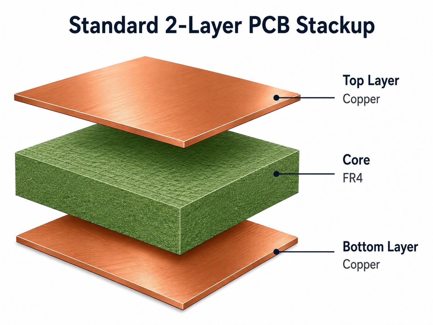
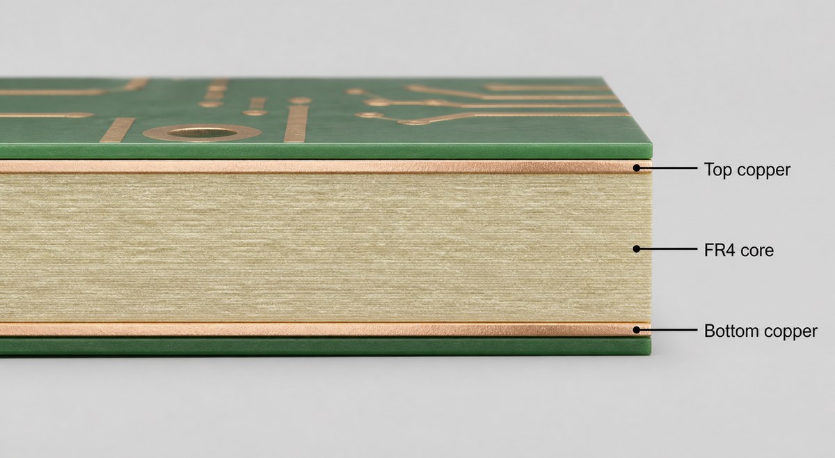
A standard 2 layer PCB stackup is usually built with copper on both sides of an FR4 PCB core. The top layer may carry components, signals, power traces, and local ground copper. The bottom layer may provide additional routing, ground return paths, power routing, and connector connections.
2 layer PCB stackup
A 2 layer PCB usually includes top copper, an FR4 core, and bottom copper, with solder mask and surface finish added during production.
LayerPractical Role
Top solder maskProtects copper and defines solderable openings
Top copperComponents, signals, power, or ground copper
FR4 coreInsulation and mechanical support
Bottom copperRouting, return paths, connectors, or ground copper
Bottom solder maskCopper protection and solder control

The stackup may be simple, but the production result still depends on material availability, copper thickness, finished board thickness, drilling, solder mask registration, surface finish, and panelization. A two layer board should not be treated as a board with no engineering risk.

1.6mm 2 Layer PCB Stackup and Copper Weight

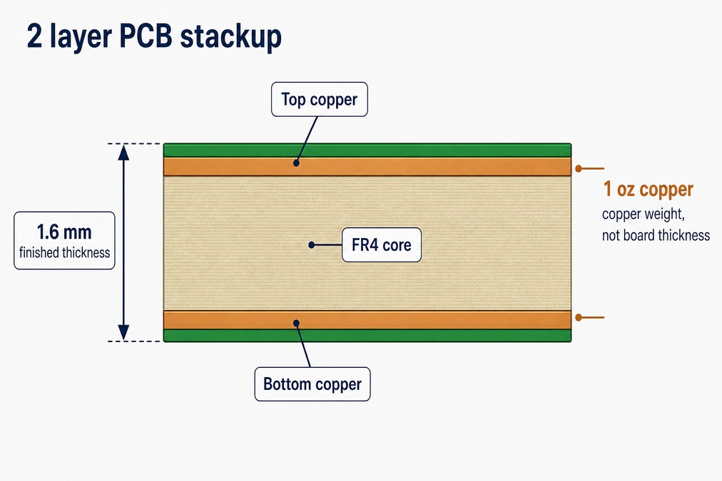
Many 2 layer PCB projects use a 1.6 mm finished board thickness because it is widely supported, mechanically stable, and compatible with many connectors and enclosures. However, 1.6 mm should refer to the finished board thickness, not only the raw laminate thickness.
2 layer PCB stackup
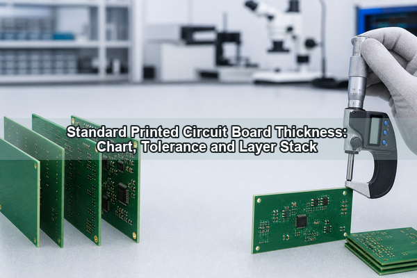
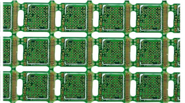
Finished board thickness is measured from the top surface to the bottom surface; copper weight is a separate specification.

Copper weight is a different requirement. For example, 1 oz copper describes the copper thickness or copper weight used on the conductive layers. It does not mean the whole board is 1 oz thick. This distinction matters when a drawing includes both board thickness and copper thickness.

Before production, confirm these thickness-related details:

  • finished board thickness and tolerance;
  • top and bottom copper weight;
  • whether copper is base copper or finished copper;
  • surface finish requirement;
  • connector or enclosure thickness limits;
  • whether impedance or current capacity depends on the stackup.

2 Layer PCB Stackup for Signal, Power, and Ground Routing

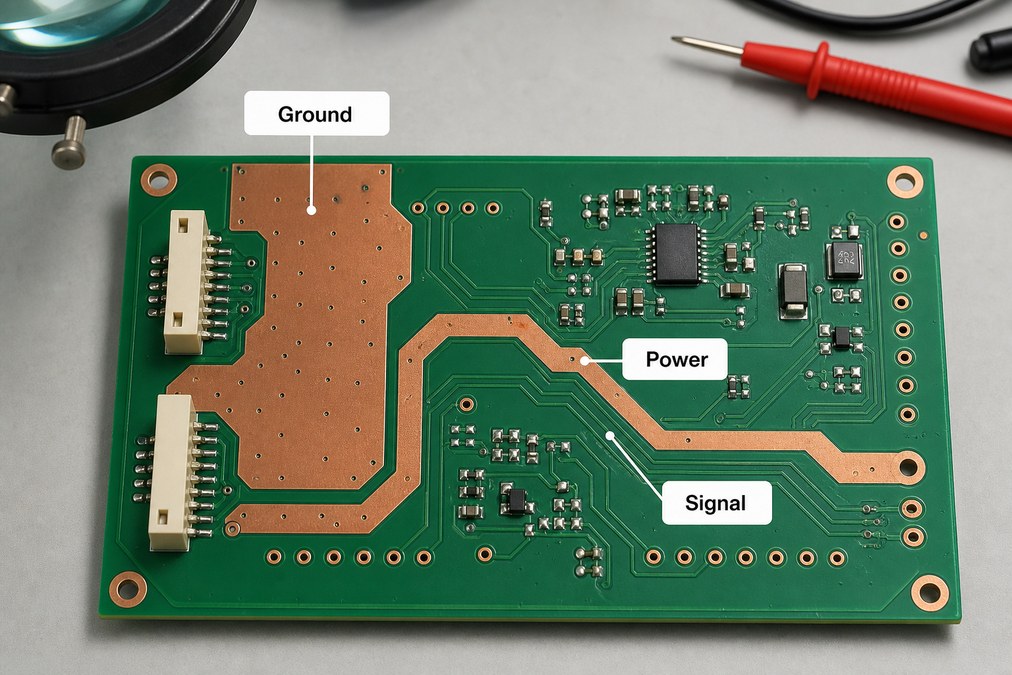
A 2 layer PCB gives less routing freedom than a 4 layer board, so the signal, power, and ground strategy must be practical. If the board has simple low-speed signals, connectors, LEDs, sensors, or basic control circuits, a two layer structure may be enough. If the board has high-speed interfaces, dense BGAs, strict EMI requirements, or multiple power domains, the project may need more review.
2 layer PCB stackup
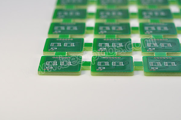
Signal, power, and ground routing should be planned early on a 2 layer PCB because routing space is limited.

For many 2 layer boards, production review focuses on:

  • return path continuity for important signals;
  • wide enough power traces for current paths;
  • clear ground copper and via stitching where needed;
  • connector orientation and pin mapping;
  • thermal relief, copper balance, and solderability;
  • test points and inspection access after assembly.

The PCB manufacturer should not change the customer’s circuit intent. EBest Circuit can review whether the approved files are manufacturable and whether the stackup, copper, drilling, solder mask, and assembly notes are clear enough before production.

2 Layer PCB Stackup vs 4 Layer PCB Stackup

A 2 layer PCB stackup is often a good choice when the project needs a lower-cost board, simple routing, fast prototype validation, or a compact control board without strict high-speed requirements. A 4 layer stackup is usually considered when the board needs better power distribution, cleaner ground reference, controlled impedance, denser routing, or improved EMI behavior.

Item2 Layer PCB4 Layer PCB
Layer structureTop and bottom copperTwo outer layers plus inner planes
Routing spaceLimited but cost-effectiveMore routing freedom
Ground referenceDepends on copper planningUsually stronger with inner plane
CostLowerHigher
Best fitSimple to moderate circuitsDense, faster, or noise-sensitive boards

The right choice depends on the product, not only the layer count. If the 2 layer board can meet routing, grounding, thermal, and assembly needs, it may be the better commercial choice. If the board is already crowded or unstable, moving to 4 layers may save debugging time later.

Manufacturing Checks Before 2 Layer PCB Fabrication

A 2 layer PCB may be easier to manufacture than a high-layer-count board, but file review still matters. A small missing note can lead to wrong thickness, wrong surface finish, solder mask mismatch, connector fit problems, or assembly delay.

EBest Circuit typically checks:

  • Gerber or ODB++ file completeness;
  • drill file and plated-through-hole requirements;
  • finished board thickness and tolerance;
  • copper weight and current-related traces;
  • minimum line width, spacing, annular ring, and solder mask opening;
  • surface finish and solderability requirement;
  • panelization, tooling holes, fiducials, and breakaway method;
  • test requirement and outgoing inspection notes.

This review is useful because the buyer receives a finished PCB, not a file screenshot. The file must be translated into a real board that can be drilled, plated, etched, solder-masked, finished, tested, packed, and assembled.

SMT and PCBA Risks on 2 Layer PCB Boards

If the 2 layer PCB also needs SMT assembly, the stackup should be reviewed together with assembly data. Board thickness, panel size, component placement, solder mask openings, fiducials, and connector positions can all affect SMT yield. If the project also includes component sourcing, the BOM should be checked before SMT scheduling.

Before assembly, the useful files include:

  • Gerber or ODB++ files;
  • BOM with approved part numbers;
  • CPL or pick-and-place file;
  • assembly drawing;
  • polarity and orientation notes;
  • panelization drawing;
  • testing and packing requirements.

For prototype and small-batch PCBA projects, EBest Circuit can review PCB fabrication and SMT assembly together. This helps keep board thickness, panelization, component sourcing, soldering, inspection, and packing notes visible under one workflow. This is especially useful when the project is still in prototype PCB assembly validation.

EBest Circuit 2 Layer PCB Stackup Manufacturing Capabilities

EBest Circuit supports 2 layer FR4 PCB projects from prototype to small-batch and production runs. The practical value is not only making a bare board, but helping the customer confirm the production path before the order moves forward.

RequirementEBest Circuit Support
Board type2 layer FR4 PCB and double sided PCB
Thickness reviewFinished thickness and tolerance confirmation
Copper optionsCommon 1 oz or higher copper review by project
Surface finishHASL, lead-free HASL, ENIG, OSP, and other options
AssemblySMT, through-hole, mixed assembly, and inspection
DocumentsDFM notes, stackup confirmation, test reports when required

EBest Circuit (Best Technology) has worked in PCB and PCBA manufacturing since 2006 and serves customers in more than 40 countries and regions. For customers comparing suppliers, stable engineering communication is often as important as the quote itself, especially when the project needs both PCB fabrication and assembly.

2 Layer PCB Stackup Case Study for a Prototype Build

A USA customer needed a small-batch 2 layer PCB prototype for a compact control board. The board looked simple at first, but the project still had several details that could affect assembly and validation.

Project snapshot:

  • Customer region: USA;
  • Application: compact control and sensor interface board;
  • Quantity: 50 pcs prototype build;
  • PCB type: 2 layer FR4 PCB;
  • Finished thickness: 1.6 mm +/-10%;
  • Copper: 1 oz top and bottom copper;
  • Surface finish: lead-free HASL;
  • Assembly: SMT after PCB fabrication;
  • Delivery focus: prototype validation before the next small batch.

What EBest Circuit reviewed before production:

  • stackup, copper weight, board thickness, and solder mask notes;
  • panelization method for SMT handling;
  • BOM availability and approved part numbers;
  • component polarity, connector direction, and placement data;
  • electrical test before assembly and visual inspection after SMT;
  • single-board packing after assembly to reduce handling damage.

The useful result for the customer was a clearer prototype path. The order quantity was small, but the board still moved through file review, PCB fabrication, SMT preparation, inspection, and packing as one controlled project. That is the kind of support that helps engineering teams validate a 2 layer PCB before scaling the design.

FAQs About 2 Layer PCB Stackup

1. Is a 2 layer PCB stackup the same as a double sided PCB?
In most PCB manufacturing contexts, yes. A double sided PCB usually means a 2 layer PCB with copper on both the top and bottom sides.

2. What is the standard thickness for a 2 layer PCB?
Many 2 layer FR4 boards use 1.6 mm finished thickness, but 0.8 mm, 1.0 mm, 1.2 mm, and other thicknesses may also be used depending on the product.

3. Is 1 oz copper the same as 1.6 mm PCB thickness?
No. 1 oz copper describes the copper layer weight or thickness. 1.6 mm describes the finished board thickness from the top surface to the bottom surface.

4. Can a 2 layer PCB stackup support controlled impedance?
Some 2 layer boards can support impedance requirements, but the stackup, trace width, dielectric thickness, copper thickness, and test requirement should be reviewed before fabrication.

5. What files should I send for a 2 layer PCB quotation?
Send Gerber or ODB++ files, drill files, stackup or thickness notes, BOM, CPL, assembly drawing, surface finish requirement, quantity, test notes, and packing requirements.

All in all, a 2 layer PCB stackup should be clear before production begins. If your project needs 2 layer FR4 PCB fabrication, thickness review, copper confirmation, SMT assembly, or prototype-to-small-batch support, please send your Gerber files, BOM, CPL, drawings, and project notes to sales@bestpcbs.com. EBest Circuit can help review the manufacturing and assembly path before your boards move into production.

You may also like

4 Layer vs 2 Layer PCB
Tuesday, July 7th, 2026

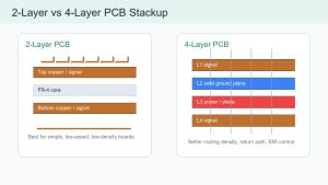
A 2 layer PCB is usually the right choice for simple, low-speed, low-density circuits where bare-board cost matters most. A 4 layer PCB is usually the better choice when the design needs cleaner return paths, better EMI control, easier routing, stronger power distribution, or more reliable high-speed behavior.

The practical decision is not only “two layers are cheaper” or “four layers are better.” The best layer count depends on circuit density, signal edge speed, power integrity, board size, EMC risk, connector placement, assembly yield, and the cost of redesign if the first prototype fails.

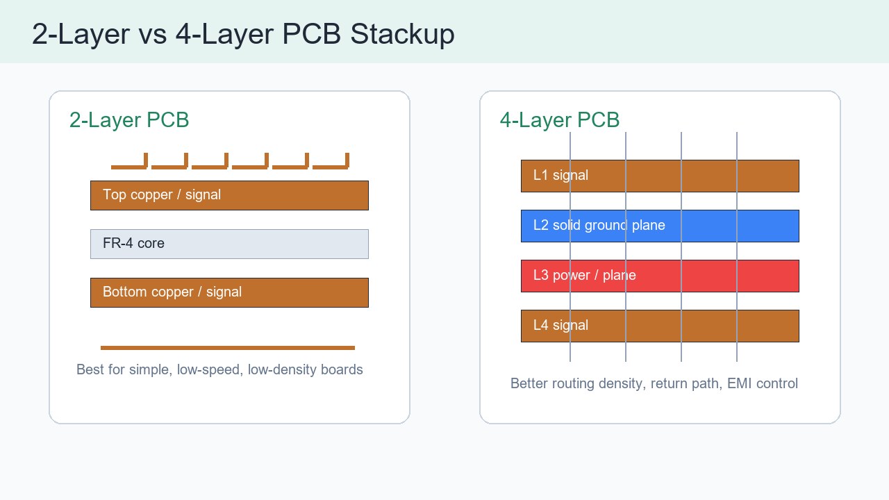
Side by side stackup comparison of a 2 layer PCB and a 4 layer PCB
2 layer and 4 layer PCB stackups differ most in routing space, plane structure, and return-current control.

Quick Answer: Choose 2 Layer for Simplicity, 4 Layer for Performance Margin

Choose a 2 layer PCB when the circuit is simple enough to route cleanly without cutting the ground path. Choose a 4 layer PCB when the board needs continuous reference planes, dense routing, lower loop area, or better control of EMI and signal integrity.

Decision Factor 2 Layer PCB 4 Layer PCB Engineering Note
Best fit Simple control boards, LED boards, basic power boards, low-speed sensors MCU boards, wireless products, mixed-signal boards, compact electronics Layer count should follow routing and noise risk, not habit.
Routing density Limited to top and bottom copper Outer routing plus inner reference and power planes 4 layers often reduce routing compromises.
EMI control Depends heavily on layout discipline and ground pours Easier to maintain short return paths with a solid plane Continuous reference planes reduce loop area.
Cost Lower bare-board cost Higher bare-board cost, sometimes lower debug cost For dense designs, 4 layers may save engineering time.
Manufacturing risk Easy to inspect and fabricate Needs stackup control, lamination, and clearer documentation Ask for stackup, impedance, and inspection requirements early.

What Is a 2 Layer PCB?

A 2 layer PCB has copper on the top and bottom sides of the board, separated by an insulating core. It can route signals on both sides, use vias to change layers, and use copper pours for ground or power distribution.

Two-layer boards are common in basic industrial controls, small LED products, simple power distribution, connector adapters, low-speed sensor boards, and cost-sensitive prototypes. The main limitation is that every trace, via, connector, and copper pour competes for the same two copper layers.

What Is a 4 Layer PCB?

A 4 layer PCB has four copper layers separated by dielectric material. A common structure is top signal, inner ground plane, inner power plane, and bottom signal, although the best stackup should be confirmed with the PCB manufacturer and the design requirements.

The main advantage is not only “more routing layers.” A 4 layer PCB can place signal traces close to a continuous reference plane, which gives return current a predictable path and helps reduce radiation, crosstalk, and ground bounce. This is why many compact digital products start at four layers even when the schematic looks moderate.

2 Layer vs 4 Layer PCB Stackup Differences

The biggest stackup difference is that a 4 layer board can dedicate inner copper to planes, while a 2 layer board must share copper for signals, power, and ground. That changes the way current returns, how decoupling capacitors behave, and how easily the layout can pass EMC testing.

Stackup Item 2 Layer PCB 4 Layer PCB Buyer or Engineering Note
Typical layers Top copper and bottom copper Top signal, ground plane, power or plane layer, bottom signal Actual construction varies by supplier and thickness.
Reference plane Ground pour may be interrupted by routing Solid inner ground plane is practical Ask whether critical signals cross plane splits or voids.
Power distribution Wider traces or pours are needed Power plane or large inner copper can reduce impedance High-current boards still need thermal and copper-width checks.
Impedance control Harder and less predictable More practical with controlled dielectric and planes Request impedance coupon and stackup data when required.
Board thickness Often simple standard thickness Needs defined dielectric and copper arrangement Confirm finished thickness, copper weight, and tolerance.

When a 2 Layer PCB Is the Better Choice

A 2 layer PCB is better when the circuit can be routed with clean grounding, enough spacing, and no high-speed or EMI-critical constraints. It is also attractive when the product needs a simple bare board, a low prototype cost, or very easy visual inspection.

  • The board has low-speed digital signals, simple analog paths, or basic switching.
  • The board size is not tightly constrained, so wider traces and ground pours fit.
  • The product is cost-sensitive and does not need controlled impedance.
  • The design has low component density and no fine-pitch BGA or dense connector field.
  • The EMC environment is mild and the enclosure, cable, and power system are simple.

A good 2 layer design still needs disciplined grounding. Avoid narrow ground traces, long return loops, poor decoupling placement, and random copper islands that look like ground but do not provide a reliable return path.

When a 4 Layer PCB Is the Better Choice

A 4 layer PCB is better when the board needs routing freedom and electrical margin. The additional layers help the designer maintain a continuous reference plane, route around dense components, and separate power distribution from sensitive signal paths.

  • The board includes fast digital edges, USB, Ethernet, RF modules, DDR, high-speed ADCs, or dense MCU routing.
  • Ground return paths are broken or difficult to control on a 2 layer layout.
  • The product must reduce EMI risk before compliance testing.
  • The PCB must be compact, connector-heavy, or packed with fine-pitch components.
  • The design needs a stable power distribution network and better decoupling behavior.

For many commercial products, 4 layers are used because the extra bare-board cost is smaller than the risk of a failed EMC test, unstable prototype, or repeated layout cycle.

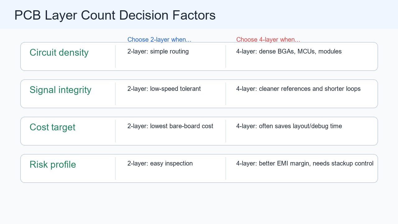
Decision factors for choosing between a 2 layer PCB and a 4 layer PCB
Layer count selection should compare circuit density, signal integrity, cost target, and project risk together.

Cost Difference: Bare Board Price vs Total Project Cost

A 2 layer PCB usually has the lower bare-board price, but a 4 layer PCB can lower total project cost when it prevents redesign, noise troubleshooting, or EMC failure. Procurement should compare the full cost of the design decision, not only the first PCB quotation.

Cost Area 2 Layer PCB Impact 4 Layer PCB Impact What to Check Before Ordering
Bare PCB fabrication Usually lower Usually higher due to lamination and extra copper layers Compare quantity, size, copper weight, finish, and delivery time.
Layout time Can increase if routing is congested Often easier for dense boards Ask whether the designer is forcing a 2 layer board too far.
EMI debugging Higher risk on noisy or cable-connected products Lower risk when planes and decoupling are designed well Consider EMC test cost and project schedule impact.
Assembly yield Good for simple boards Good when routing supports clean placement and test access Check test points, panelization, and soldering access.
Future revisions May need a layer-count upgrade later More margin for product updates Consider whether the product roadmap adds functions.

Signal Integrity and EMI: Why Ground Planes Matter

Signal integrity and EMI are often the reason a design moves from 2 layers to 4 layers. A solid ground plane under signal traces gives return current a short path, reduces loop area, and helps contain electromagnetic fields.

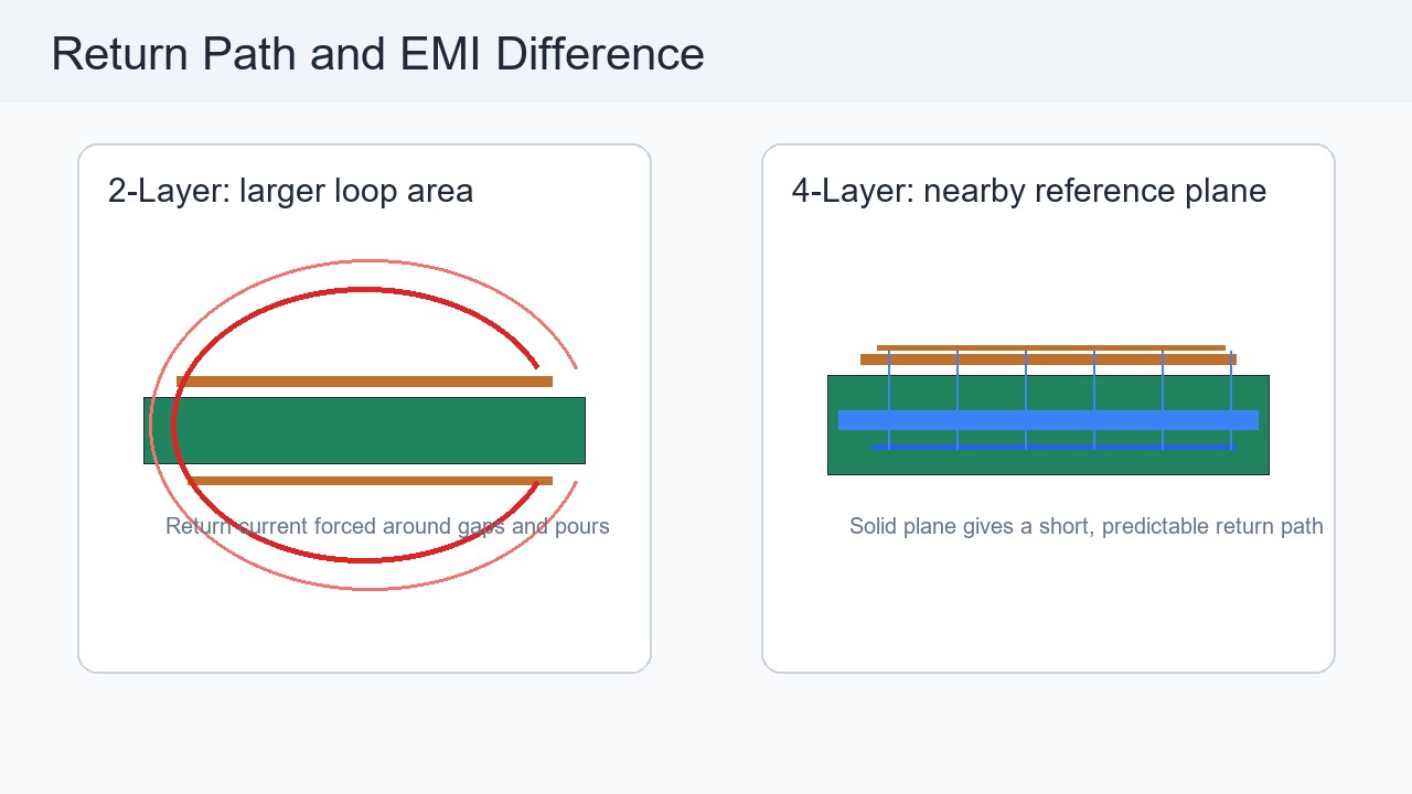
On a 2 layer board, ground pours can help, but they are frequently cut by routing channels, vias, slots, connectors, and power traces. When the return path has to detour, the loop area grows. Larger loops are more likely to radiate noise and pick up noise from nearby switching circuits.

Return path and EMI comparison between 2 layer and 4 layer PCB layouts
A 4 layer PCB can keep signal traces close to a continuous reference plane, reducing loop area and EMI risk.

Routing Density and Component Placement

A 4 layer PCB makes routing easier when components are dense, but it does not replace good placement. Put connectors, power sections, clocks, high-current paths, and sensitive analog areas in logical zones before deciding whether two layers are enough.

For a 2 layer design, routing congestion often causes long traces, extra vias, narrow ground necks, and poor test-point access. For a 4 layer design, routing can be cleaner, but the designer must still avoid plane splits under critical signals and document which layers are used for reference and power.

Manufacturing and Quality Control Differences

A 2 layer PCB is simpler to fabricate, while a 4 layer PCB needs tighter control of lamination, registration, dielectric thickness, and stackup documentation. This does not make 4 layer boards risky, but it does mean the supplier should receive clearer fabrication notes.

  • Confirm finished thickness, copper weight, solder mask, surface finish, and impedance requirements.
  • For 4 layer boards, request the stackup before fabrication if impedance, EMI, or mechanical thickness matters.
  • Use IPC-A-600 and IPC-6012 acceptance class requirements when they are part of the buyer’s quality specification.
  • Check annular ring, drill tolerance, minimum trace/space, solder mask bridge, and via fill or tenting requirements.
  • Keep test points accessible, especially when the 4 layer design is dense and assembled with fine-pitch parts.

Common Mistakes When Choosing Layer Count

The most common mistake is choosing the layer count by price alone. Another common mistake is assuming that a 4 layer PCB automatically fixes EMI, even when the stackup has poor reference planes or signals cross plane gaps.

Mistake Why It Matters Better Decision
Forcing dense routing onto 2 layers Creates long traces, broken ground paths, and hard-to-debug noise Compare 4 layer cost against redesign and EMC risk.
Using 4 layers without a clear stackup Planes may not support the signals that need them Define layer order, reference plane, and dielectric targets.
Ignoring power return paths High-current loops can heat copper and radiate noise Review power width, copper weight, via count, and thermal path.
Comparing quotes with different specs Price differences may come from finish, copper, test, or delivery Use the same Gerber, stackup, quantity, finish, and test requirements.
Skipping DFM review Small layout problems can become production defects Ask the PCB supplier for DFM feedback before mass production.

Procurement Checklist Before Ordering 2 Layer or 4 Layer PCB

Procurement should ask technical questions before comparing price, because layer count affects quality requirements, lead time, and manufacturing control. A clear RFQ reduces quotation errors and avoids surprise engineering changes.

  • What is the finished board thickness and tolerance?
  • What copper weight is required on outer and inner layers?
  • Does the design require controlled impedance or impedance testing?
  • What minimum trace/space, drill size, annular ring, and solder mask bridge are used?
  • Is electrical test required for every board?
  • Are there high-current, RF, high-speed, or mixed-signal areas that need engineering review?
  • Does the supplier provide DFM feedback before production?
  • For 4 layer PCB, can the supplier confirm the proposed stackup before fabrication?

Best Practical Selection Rule

The best rule is to use 2 layers only when the board remains electrically clean, manufacturable, and easy to test. Use 4 layers when the design needs a controlled reference plane, better routing density, or more performance margin than a 2 layer layout can provide.

For early prototypes, a 2 layer board may be enough to validate a simple circuit. For products with cables, switching power, fast digital interfaces, dense modules, or EMC exposure, starting with 4 layers often produces a cleaner design path.

FAQ About 4 Layer vs 2 Layer PCB

Is a 4 layer PCB always better than a 2 layer PCB?

No. A 4 layer PCB is usually better for dense routing, EMI control, and signal integrity, but a 2 layer PCB can be the better choice for simple, low-speed, cost-sensitive designs.

When should I upgrade from 2 layer to 4 layer PCB?

Upgrade when routing is congested, return paths are broken, EMI risk is high, impedance control is needed, or the board includes dense ICs, fast edges, wireless modules, or mixed-signal sections.

Is a 4 layer PCB much more expensive?

It is usually more expensive as a bare PCB because it needs more copper layers and lamination. However, the total project cost can be lower if 4 layers reduce redesign, EMI debugging, or layout time.

Can a 2 layer PCB pass EMI testing?

Yes, many 2 layer boards can pass EMI testing when the layout, grounding, filtering, enclosure, and cable design are well controlled. The risk rises when the board has fast edges, switching power, long cables, or broken return paths.

What is the common 4 layer PCB stackup?

A common stackup is signal, ground plane, power plane, and signal. Some designs use two ground reference layers or different plane arrangements. The right stackup should be confirmed with the manufacturer and the design requirements.

Is a 2 layer PCB suitable for LED products?

Often yes. Simple LED boards can use 2 layers when current, heat, copper width, and voltage drop are controlled. High-power LED boards may need heavier copper, metal-core PCB, or special thermal design instead of simply adding layers.

Does a 4 layer PCB improve heat dissipation?

It can help spread heat when inner copper planes are designed as part of the thermal path, but layer count alone is not a thermal solution. Copper weight, via arrays, board material, component placement, and enclosure contact matter more.

Can I route high-speed signals on a 2 layer PCB?

Some moderate-speed designs can work on 2 layers, but high-speed signals become harder to control because the return path and impedance are less predictable. For reliable high-speed interfaces, 4 layers are usually a safer starting point.

Do I need controlled impedance for every 4 layer PCB?

No. Controlled impedance is needed when the interface or signal speed requires it. If needed, specify impedance values, tolerance, layer reference, stackup, and test requirements in the fabrication notes.

Which is better for prototypes, 2 layer or 4 layer PCB?

Use 2 layers for simple proof-of-concept prototypes where cost and speed matter. Use 4 layers when the prototype must represent real EMI, signal integrity, power integrity, and product-size constraints.

Can a 4 layer PCB make assembly harder?

Layer count itself does not usually make assembly harder, but dense 4 layer layouts may reduce test access and increase placement complexity. Keep test points, fiducials, panelization, and soldering clearance in the DFM review.

What should I send to a supplier for a 4 layer PCB quote?

Send Gerber files, drill files, BOM if assembly is required, stackup requirements, finished thickness, copper weight, surface finish, impedance requirements, solder mask color, quantity, test requirements, and delivery expectations.

Final Recommendation

For a simple low-speed board, 2 layers can be the most economical and practical choice. For dense electronics, high-speed interfaces, EMI-sensitive products, compact layouts, or production designs where failure is expensive, 4 layers usually provide better engineering margin.

If you’re sourcing reliable PCB/PCBA manufacturing, including OEM, ODM, prototyping, mass production, or custom engineering solutions, reach out to our engineering team for technical support and a quote at sales@bestpcbs.com.

You may also like

Reliable Double Layer PCB Manufacturing for Prototype and Mass Production
Thursday, June 25th, 2026

Double layer PCB manufacturing is a common choice for electronic products that need more routing space than a single-sided PCB, but do not require the cost or complexity of a multi-layer PCB. This guide explains double layer PCB manufacturing from an engineering and purchasing point of view. It covers the structure, stackup, materials, manufacturing process, layout rules, applications, real production cases, and supplier selection.

Best Technology supports reliable double layer PCB manufacturing from prototype to mass production, with practical process capability for standard FR4, High Tg FR4, FPC, aluminum PCB, and PCB assembly projects. For 2 layer PCB production, we can support common board thicknesses, 1 oz and higher copper options, ENIG, HASL, OSP, immersion silver, immersion tin, and other surface finishes. Our process capability also covers fine line/space, PTH via plating, controlled hole tolerance, solder mask alignment, and SMT panel requirements. If you are developing a new double layer PCB project, pls feel free to send your Gerber files, BOM, stackup, or sample photos to sales@bestpcbs.com. Our engineering team can review your files and provide a practical quotation.

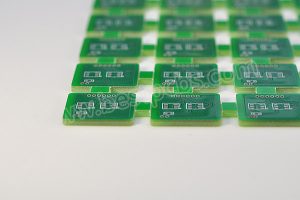
Double layer PCB manufacturing

What Is Double Layer PCB Manufacturing?

Double layer PCB manufacturing is the process of producing a printed circuit board with copper circuits on both the top and bottom sides. These two copper layers are connected by plated through holes, also called PTH vias, so signals and current can pass between the two sides.

A double layer PCB is also called a double sided PCB, D/S PCB, 2L PCB, 2 layer PCB, or double layer printed circuit board. Unlike a single-sided PCB, it has two conductive layers and supports routing on both sides. Components can also be assembled on one side or both sides, depending on the design and assembly requirements.

The main advantage is better routing flexibility. A 2 layer PCB gives engineers more space for traces, vias, power lines, and component placement, while keeping the cost lower than a 4 layer PCB. For this reason, double layer PCB manufacturing is widely used for prototypes, small batches, and mass production of control boards, sensor modules, power interface boards, and general electronic products.

How Is a Double Layer Printed Circuit Board Structured?

A double layer printed circuit board has a simple structure, but each layer has a clear function. A standard FR4 double layer PCB usually includes solder mask, copper traces, core material, surface finish, and silkscreen on both sides.

StructureFunction
SilkscreenMarks
Surface finishSolderability
Solder maskProtection
Top copperCircuit
FR4 coreInsulation
Bottom copperCircuit
PTH viaLayer connection

The most important part is the PTH via. The hole wall is plated with copper, so the top and bottom copper layers can connect electrically. Without PTH vias, the two sides cannot work as one circuit.

A conventional 2 layer PCB does not use blind vias or buried vias. These structures are normally used in more complex multilayer PCBs. For most double layer PCB manufacturing projects, standard through vias are enough.

What buyers should confirm

Before production, buyers should make sure the hole type is clear. PTH holes are used for electrical connection. NPTH holes are usually used for mounting, positioning, or mechanical support. If this information is unclear, the board may be produced incorrectly.

Buyers should also check via size, annular ring, solder mask opening, board outline, and whether the board needs SMT, DIP, or mixed assembly.

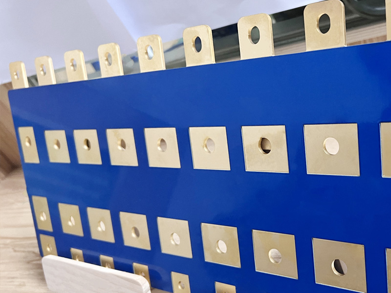
What Is the Standard 2 Layer PCB Stackup?

A standard 2 layer PCB stackup is usually simple. It has top copper, core material, and bottom copper. Solder mask, silkscreen, and surface finish are added during production.
Double layer PCB manufacturing

A common 2 layer PCB stackup uses FR4 material, 1.6 mm finished thickness, 1 oz copper, green solder mask, white silkscreen, and HASL or ENIG surface finish. This is a widely used configuration for many standard electronic products.

However, the stackup can be adjusted. The finished thickness may be 0.8 mm, 1.0 mm, 1.2 mm, 1.6 mm, or 2.0 mm. Copper thickness can also change based on current load and thermal needs.

OptionCommon Use
0.8–1.2 mmThin boards
1.6 mmStandard
2.0 mmStronger support
0.5 ozFine circuits
1 ozGeneral use
2 oz+Higher current

Stackup selection should not be based only on price. It should match current load, board size, component weight, assembly method, operating temperature, and mechanical strength.

For simple control circuits, a standard 1.6 mm FR4 stackup is often enough. For industrial or power products, thicker copper, High Tg FR4, or a stronger board thickness may be a better choice.

What Materials Are Used in a 2 Layer Printed Circuit Board?

FR4 is the most common material used in 2 layer printed circuit boards. It offers stable insulation, good mechanical strength, and reasonable cost. This is why it is widely used in control boards, consumer electronics, industrial devices, and general electronic products.

Different applications may need different materials. A product with higher temperature stress may need High Tg FR4. A flexible connection may need PI material. A lighting product with thermal requirements may need aluminum substrate.

MaterialBest For
FR4General PCB
High Tg FR4Heat resistance
CEM-1/CEM-3Cost-sensitive
FR5Higher heat
PIFPC
AluminumHeat dissipation

Surface finish is also part of the material decision. It protects exposed copper and affects solderability. Common options include HASL, lead-free HASL, ENIG, OSP, immersion silver, and immersion tin.

FinishAdvantage
HASLLow cost
Lead-free HASLRoHS
ENIGFlat surface
OSPSMT friendly
Immersion silverGood soldering
Immersion tinFlat pads

ENIG is often used when the design has fine-pitch SMT pads, small components, or higher solderability requirements. HASL is suitable for many standard products and is often more economical.

Buyer note

Material choice should consider working temperature, soldering process, shelf life, current load, assembly complexity, and product reliability. Choosing the right material early can reduce production risk later.

How Does the Double Layer PCB Manufacturing Process Work?

The double layer PCB manufacturing process includes file review, material preparation, drilling, plating, imaging, etching, solder mask, surface finish, profiling, and testing. Each step must be controlled because one weak process can affect the whole board.

Step 1: Engineering file review

  • The manufacturer checks Gerber files, drill files, board outline, copper thickness, surface finish, solder mask color, and special notes. A good DFM review can catch missing drill files, small annular rings, unclear slots, copper too close to the board edge, and panel design problems before production starts.

Step 2: Material preparation

  • The factory prepares the copper clad laminate according to the required material, thickness, and copper weight. The panel size is planned based on board dimensions, quantity, and production efficiency.

Step 3: Drilling

  • Holes are drilled according to the drill file. These holes may include vias, component holes, mounting holes, positioning holes, and slots. Drilling accuracy is important because hole shift can reduce the annular ring and affect reliability.

Step 4: PTH plating

  • After drilling, the hole wall is not conductive. The factory deposits and plates copper inside the hole wall to form a plated through hole. This step connects the top and bottom copper layers.

Step 5: Circuit imaging and etching

  • The circuit pattern is transferred to the copper surface through dry film imaging. After plating and etching, unwanted copper is removed, and the final circuit pattern remains. Etching must be controlled well. Over-etching makes traces too narrow, while under-etching may cause shorts.

Step 6: Solder mask and surface finish

  • Solder mask protects the copper surface and reduces solder bridging during assembly. Surface finish protects exposed pads and improves solderability. The finish should match the assembly process and storage requirements.

Step 7: Profiling and testing

  • The board is routed, V-cut, or milled to shape. Then it goes through electrical test and final inspection. Common checks include open/short test, hole quality, solder mask alignment, surface finish, dimensions, and appearance.

Manufacturing tip

  • Prototype projects usually focus on speed and design validation. Mass production focuses more on repeatability, yield, panel stability, and delivery consistency. A good manufacturer should support both stages.

What PCB Layout Rules Should Be Checked Before Double Layer PCB Manufacturing?

Good PCB layout makes manufacturing easier and more reliable. Before sending files to production, engineers should check trace width, spacing, via design, hole type, copper balance, solder mask, silkscreen, and panelization.

Trace width and spacing

  • Signal traces can be narrow, but power traces need enough width to carry current. Spacing must match voltage and manufacturing capability. Copper-to-edge clearance should also be checked to avoid exposed copper after routing.

Via size and annular ring

  • Vias need enough drill size and pad size. A small annular ring leaves little tolerance for drilling shift. This can affect hole reliability, especially during batch production.

PTH and NPTH definition

  • PTH means plated through hole. NPTH means non-plated through hole. Mounting holes are often NPTH, while electrical holes are usually PTH. This definition should be clear in the drill file or fabrication notes.

Copper balance

  • Copper should be balanced on both sides of the PCB. Large copper imbalance may cause warpage, especially on thin boards, large panels, heavy copper boards, and SMT panels.

Solder mask and silkscreen

  • Solder mask openings should match pad design. Fine-pitch components need enough solder mask bridge. Silkscreen should not cover solder pads because ink on pads may affect soldering.

Panelization for SMT

  • If the board needs SMT assembly, panel design becomes important. The panel may need tooling holes, fiducial marks, process edges, V-cut, routing tabs, and a correct feeding direction.

Buyer tip

Do not only ask for a PCB price. Ask the supplier to review manufacturability. A simple DFM check before production can prevent many costly changes.

When Should You Choose a 2 Layer Circuit Board?

A 2 layer circuit board is a good choice when the circuit has moderate complexity and can be routed on two sides. It is also suitable when cost, lead time, and production simplicity are important.

Choose 2 Layer WhenReason
Medium densityEasy routing
Moderate speedBasic SI enough
Cost-sensitiveLower cost
Prototype stageFast validation
No blind viasSimple process
Basic groundingCopper pour works

A 2 layer PCB is commonly used in control boards, sensor boards, LED control boards, power interface boards, consumer electronics, industrial terminal boards, and prototype boards. It gives enough routing flexibility for many designs while keeping cost under control.

However, 2 layers may not be enough for high-speed interfaces, dense BGA components, strict EMI control, controlled impedance, complex power networks, or very small board sizes. In those cases, a 4 layer PCB may provide better routing, grounding, and signal performance.

Simple decision rule

Use a 2 layer PCB when the circuit is simple to medium in complexity. Move to 4 layers when routing, EMI, or signal quality becomes difficult.

What Are the Common Applications of Double Layer PCBs?

Double layer PCBs are used across many industries because they balance cost, function, and manufacturability. They are especially suitable for products that need more routing space than a single-sided board but do not need a complex multilayer structure.

Consumer electronics

  • Double layer PCBs are used in chargers, audio devices, remote controls, small appliances, smart home products, and display control boards. These products need stable performance and controlled cost.

Industrial control

  • Industrial boards often use connectors, terminals, relays, sensors, and microcontrollers. A double layer PCB can support these parts well, especially when the design uses both SMT and through-hole components.

LED and lighting products

  • Some LED driver boards and lighting control boards use double layer PCBs. If the product has higher thermal requirements, aluminum PCB may be a better option. The choice depends on LED power, heat path, housing design, and assembly method.

Power and battery products

  • Charging boards, battery protection boards, low-power supply boards, and power interface modules can use 2 layer PCBs when current and thermal requirements are manageable. Wider traces and thicker copper may be needed.

Automotive auxiliary electronics

  • Some automotive auxiliary products use double layer PCBs, such as lighting control boards, sensor interfaces, small control modules, and in-car accessories. Material and reliability checks are important for these projects.

2L FPC applications

  • A 2L FPC also uses a two-layer circuit structure, but it is flexible rather than rigid. It is used in wearable devices, display modules, camera modules, compact electronics, and flexible interconnections.

Double Layer PCB Case Study: From Prototype to Production

Real production cases show that 2 layer PCB projects are not always simple. Different materials, thicknesses, finishes, and assembly needs create different manufacturing risks.

Case A: 2L FR4 High Tg PCB for stable production

This case is a typical double layer FR4 PCB project with higher material requirements and panel efficiency needs.

ItemSpecification
Type2L FR4
MaterialTg170
Thickness2.0 mm ±10%
Copper1 oz
FinishENIG
Mask/TextGreen/White
ShapeØ8.5 mm
Panel236 × 119.2 mm
Array105-up

This board uses Tg170 material, which offers better heat resistance than standard FR4. The 2.0 mm thickness improves mechanical strength, while ENIG provides a flat solderable surface for stable assembly. Since the panel contains 105 pieces, the manufacturer must control panel accuracy, routing path, solder mask registration, and electrical testing.

Before mass production, the engineering team should check hole position, board outline, panel spacing, ENIG pad quality, copper balance, fiducial marks, and test method. The goal is not only to make one good sample. The goal is to keep every board stable across the full panel.

Case B: 2L FPC prototype with PI stiffener

This case is useful for flexible electronics where a rigid PCB cannot fit the product structure.

ItemSpecification
Type2L FPC
Copper1/2 oz RA
Base1 mil PI
CoverlayHalf-and-half
Thickness0.116 mm ±0.03
Stiffener0.25 mm PI
Lead time3–4 days

A 2L FPC is much thinner than a rigid FR4 PCB. It needs careful control of bend area, coverlay opening, stiffener position, copper type, and final thickness tolerance. Handling is also important because flexible circuits are easier to deform during production.

Case C: Aluminum PCB with SMT requirements

This case is not a standard FR4 double layer PCB, but it is useful for thermal applications and assembly planning.

ItemSpecification
TypeAluminum PCB
Thickness1.6 mm
Copper1 oz
Thermal1 W
Mask/TextWhite/Black
FinishLead-free HASL
AssemblySMT required

This type of project may require bare board delivery and SMT assembly in the same order. The supplier must check panel design, fiducial marks, process edges, SMT direction, BOM sourcing, remaining material return, and final delivery format.

What buyers can learn

A 2 layer PCB order should not be judged only by layer count. Material, copper weight, board thickness, surface finish, panel design, assembly needs, lead time, and testing requirements all affect manufacturing risk. Clear specifications help the project move from prototype to stable production with fewer revisions.

Double Layer PCB vs 4 Layer PCB Board: Which One Should You Choose?

Double layer PCB and 4 layer PCB are both common. The better choice depends on routing density, signal speed, EMI requirements, cost target, and product reliability.

ItemDouble Layer PCB4 Layer PCB
Layers24
CostLowerHigher
RoutingModerateBetter
EMIBasicBetter
GroundCopper pourPlane possible
Best forSimple/mediumDense/high-speed

Choose a double layer PCB when the circuit is not dense, cost is important, lead time is tight, signal speed is moderate, and basic grounding is enough. It is a strong choice for many control boards, sensor boards, interface boards, and prototypes.

Choose a 4 layer PCB when the board is small but dense, signal lines are many, EMI control is important, high-speed signals are used, or a stable ground plane is required. A 4 layer PCB can improve routing quality and electrical performance.

Do not force a complex design into 2 layers just to reduce PCB cost. A poor 2 layer layout may create noise, failed testing, assembly problems, or redesign cost. The best PCB structure should meet function, cost, reliability, and delivery needs at the same time.

Why Choose Best Technology for Double Layer PCB Manufacturing?

Best Technology supports double layer PCB manufacturing from prototype to mass production. We can help with standard FR4 PCB, High Tg PCB, 2L FPC, aluminum PCB, and PCB assembly projects.

For buyers, this reduces communication gaps between PCB fabrication, assembly, and material sourcing. For engineers, it provides practical manufacturing feedback before production starts.

RequirementSupport
PrototypeFast build
Small batchFlexible quantity
Mass productionStable quality
FR4 / High TgMaterial options
2L FPCFlex support
Aluminum PCBThermal use
AssemblySMT/DIP

Our engineering review can cover Gerber files, drill files, stackup, copper thickness, via design, annular ring, solder mask, surface finish, board outline, panelization, fiducial marks, SMT process edges, BOM, and assembly requirements.

This matters because many PCB problems do not start on the production line. They start from design details, such as unclear hole type, narrow power traces, missing fiducial marks, small via annular rings, poor solder mask bridge, or a surface finish that does not match the assembly process.

Working with one experienced supplier can simplify the project. You can manage PCB fabrication, PCB assembly, BOM sourcing, engineering review, process advice, quality inspection, and delivery planning in one place.

If you need double layer PCB manufacturing, send your Gerber files, BOM, stackup, or sample photos to sales@bestpcbs.com. Our team can review your project and provide a practical quotation.

FAQs about double layer pcb manufacturing

Q1: Is a double layer PCB the same as a 2 layer PCB?
Yes. In most cases, they mean the same thing. Both refer to a PCB with copper circuits on the top and bottom sides.

Q2: What is D/S PCB?
D/S PCB means double sided PCB. It is another name for a double layer PCB or 2L PCB.

Q3: Does a double layer PCB need PTH vias?
Yes. PTH vias are needed when the top and bottom copper layers must connect electrically.

Q4: Does a 2 layer PCB have blind vias or buried vias?
No. A conventional 2 layer PCB uses through vias. Blind vias and buried vias are used in more complex multilayer PCBs.

Q5: What is the standard 2 layer PCB stackup?
A standard stackup includes top copper, FR4 core, and bottom copper. Solder mask, silkscreen, and surface finish are added during production.

Q6: What material is best for double layer PCB manufacturing?
FR4 is the most common choice. High Tg FR4 is better for higher temperature needs. PI is used for 2L FPC. Aluminum substrate is used for thermal applications.

Q7: What copper thickness is common for a 2 layer PCB?
1 oz copper is common for standard boards. Higher copper thickness may be used for power or high-current circuits.

Q8: Can components be assembled on both sides of a double layer PCB?
Yes. Components can be assembled on the top side, bottom side, or both sides.

Q9: Is a double layer PCB cheaper than a 4 layer PCB?
Usually yes. A double layer PCB has fewer layers and a simpler structure. The final price still depends on size, material, copper thickness, finish, and quantity.

Q10: When should I choose a 4 layer PCB instead of a double layer PCB?
Choose a 4 layer PCB when the circuit is dense, high-speed, EMI-sensitive, or difficult to route on two layers.

Q11: What files are needed for double layer PCB manufacturing?
You should provide Gerber files, drill files, board outline, stackup, copper thickness, solder mask color, surface finish, and quantity. For assembly, BOM and pick-and-place files are also needed.

Q12: How can I reduce risk before double layer PCB production?
Request a DFM review before production. Check trace width, spacing, via size, annular ring, solder mask, panelization, and assembly requirements.

In conclusion, double layer PCB manufacturing is a reliable choice for many electronic products. It offers more routing space than single-sided PCB and keeps cost lower than many multilayer PCB options.

A good 2 layer PCB project starts with clear specifications. Material, copper thickness, via design, surface finish, panelization, and assembly needs should be confirmed before production.

Best Technology supports double layer PCB manufacturing from prototype to mass production. We can also help with FR4 PCB, High Tg PCB, 2L FPC, aluminum PCB, and PCB assembly.

If you have a new project, send your Gerber files, BOM, or technical requirements to sales@bestpcbs.com. Our engineering team can review your files and provide a practical quotation.

You may also like