A 2 layer PCB ground plane gives a two-layer board a stable reference for signals, power return, and noise control. It helps reduce loop area, lower ground impedance, improve EMI performance, and support more reliable circuit behavior during prototype and batch production.
However, a two-layer board has limited routing space. Signal traces, power routes, vias, connectors, and component placement can easily cut the copper reference. This guide explains how to build a practical 2 layer PCB ground plane without creating broken return paths or hidden manufacturing risks.
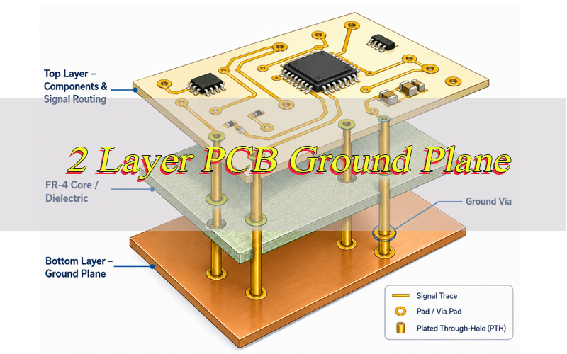
What Is a 2 Layer PCB Ground Plane?
2 Layer PCB ground plane is a grounded copper reference area used to provide a stable return path for signal current and power current. In most layouts, the bottom layer works as the main ground reference, while the top layer carries components, short traces, and power routing.
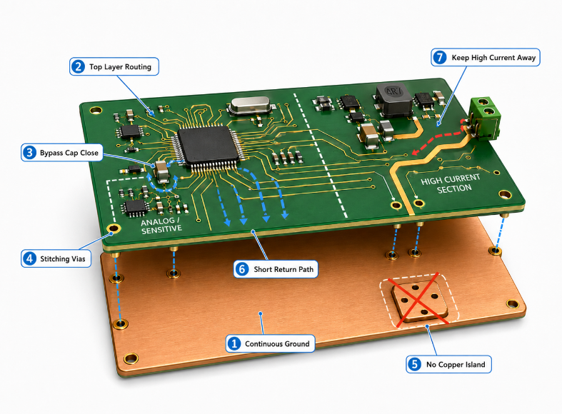
A 2 layer PCB ground plane is not just empty copper fill. It must be continuous, low impedance, and connected to every important ground point. If the copper is broken into islands, narrow necks, or separated sections, it cannot support a stable return path. Therefore, ground planning should start before signal routing.
Why Does a 2 Layer PCB Ground Plane Matter for PCB Stability?
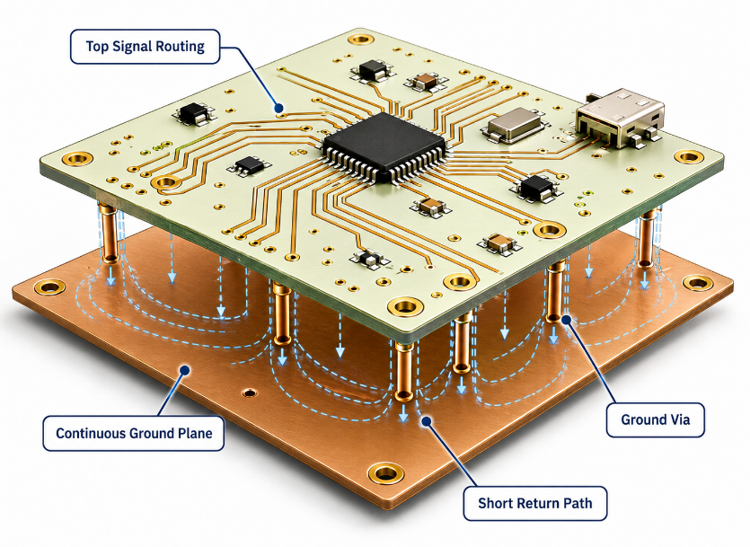
A stable ground reference reduces noise, controls EMI, and keeps signal return paths short. When the return path is close to the original trace, the loop area becomes smaller, so the board is less sensitive to EMI, crosstalk, and switching noise.
A 2 layer PCB ground plane also improves power stability. MCU pins, ADC inputs, regulators, wireless modules, and connectors all need a clean ground reference. If the ground copper is cut, return current must detour around slots and traces. As a result, the board may show voltage bounce, reset problems, unstable readings, or communication errors.
Main benefits include:
- Lower return path impedance
- Smaller signal and power loop area
- Better noise and EMI control
- More stable power reference
- Lower prototype failure risk
Should a 2 Layer PCB Ground Plane Be on the Top or Bottom Layer?
For most two-layer layouts, the bottom layer should be used as the main ground reference. The top layer usually holds components, short signal traces, and local power routing. This arrangement keeps the bottom copper more continuous and makes the return path easier to control.
Top layer ground copper can also be useful, but it should not replace the main bottom reference. It is better for local shielding, exposed pad connection, copper balance, and short ground access near components. The key point is to connect top and bottom ground copper with enough stitching vias.
| Layer | Common Use | Layout Note |
|---|---|---|
| Top | Components, signals, power | Keep traces short and organized |
| Bottom | Main ground reference | Avoid cutting the plane |
| Top Pour | Local ground copper | Stitch to bottom ground |
| Bottom Pour | Main return path | Keep it continuous |
The practical answer to PCB ground plane 2 layer top or bottom is clear: use the bottom layer as the main reference and add top ground pour only where it improves connection or copper balance.
How Should Power and Ground Be Planned on a 2 Layer PCB?
Power should be routed with wide traces or local copper, while ground should remain as continuous as possible. This is more reliable than trying to create separate 2 layer PCB power ground planes that cut routing space and weaken the ground system.
A good power layout starts from the input connector, then moves through protection parts, regulators, bulk capacitors, loads, and return paths. High-current loops should stay short and away from analog, clock, RF, and sensor areas. Meanwhile, every power rail should have a nearby ground return.
Recommended arrangement:
- Use the bottom layer as the main ground reference
- Route power with wide traces or local copper areas
- Keep input, regulator, load, and return paths close
- Keep high-current ground away from sensitive signal areas
- Use multiple vias for high-current ground transitions
- Review copper width based on current and temperature rise
This layout keeps power delivery predictable and protects the 2 layer PCB ground plane from unnecessary cuts.
How to Route a 2 Layer PCB with Ground Plane?
The safest method is to keep most signal routing on the top layer and protect the bottom ground reference. Component placement should be finished before routing. Place connectors, ICs, regulators, crystals, sensors, and high-current loads in a logical current flow.
When deciding how to route 2 layer PCB with ground plane, avoid long bottom-layer signal traces. Each long trace on the bottom layer cuts the ground reference and forces return current to take a longer route. If a signal must cross to the bottom layer, keep the trace short and return to the top layer quickly.
Good routing habits include:
- Keep most signal routing on the top layer
- Avoid long slots through the bottom ground copper
- Route related signals in the same area
- Keep clocks and fast signals away from board edges
- Avoid routing across ground gaps
- Use short paths between IC pins and support parts
A 2 layer PCB solid ground plane layout is easier to achieve when placement is clean before routing begins.
How to Use Copper Pour as a Ground Plane on a Two-Layer PCB?
Copper pour should improve ground continuity, not simply cover empty board space. On a two-layer board, ground copper should connect to the same GND net, support short return paths, and reduce broken reference areas around signals, capacitors, connectors, and power circuits.
A 2 layer PCB copper pour ground plane should be checked after every routing change. If the copper pour is separated by long traces, vias, slots, or narrow copper necks, it may look complete but still fail as a return path. Floating copper islands should be removed because they can pick up noise and create unpredictable coupling.
Copper pour best practices:
- Connect all ground pours to the same ground net
- Remove isolated copper islands
- Add stitching vias near separated copper areas
- Keep high-current ground paths wide
- Avoid thin ground necks around dense routing
- Check copper pour after routing changes
- Use top ground pour only when it connects well to bottom ground
- Avoid using copper pour to hide poor placement or broken routing
Copper pour should strengthen the 2 layer PCB ground plane by creating a lower-impedance return path, better copper balance, and cleaner ground connection across the board.
How Should Bypass Caps Connect to the Ground Plane in a 2 Layer PCB?
Bypass caps should connect to power and ground through the shortest practical loop. The capacitor should sit close to the IC power pin, and its ground side should connect directly to the ground copper through a short trace, nearby via, or direct copper connection.
For PCB 2 layer bypass caps to ground plane, the real goal is not only placing capacitors near the chip. The power pin, capacitor, ground via, and return path must form a small loop. If the capacitor ground is routed through a long thin trace, the inductance increases and the capacitor reacts more slowly.
A simple layout flow works best. First, place the capacitor next to the power pin. Then connect the power side with a short trace. Next, connect the ground side to the plane with a nearby via or direct copper. Finally, keep noisy traces away from this area.
What 2 Layer PCB Ground Plane Design Rules Should Be Followed?
The design should protect return current first, then use copper pour to support the layout. The goal is to keep ground continuous, reduce loop area, and avoid hidden noise paths before the board enters prototype or mass production.
- Keep the main ground copper continuous
The bottom layer should stay as unbroken as possible. Long signal traces, slots, and dense via channels can cut the return path and increase EMI risk. - Route most signals on the top layer
This helps protect the bottom ground reference. If a trace must use the bottom layer, keep it short and avoid cutting across critical return areas. - Place bypass caps close to IC power pins
The capacitor, power pin, and ground connection should form a small loop. A long capacitor ground trace reduces the effect of decoupling. - Use stitching vias between top and bottom ground copper
Stitching vias help connect separated copper areas and reduce ground impedance. They are especially useful near connectors, board edges, regulators, and noisy circuits. - Avoid isolated copper islands
Floating copper can pick up noise and create unpredictable coupling. Remove unused islands or connect them properly to the ground net. - Keep high-current return paths away from sensitive circuits
Motor drivers, LED loads, relays, and switching regulators should not share weak return paths with ADC, sensor, clock, or RF circuits. - Control copper width for current and heat
Narrow ground necks may pass DRC but still cause voltage drop or temperature rise. Use wider copper for load current and review copper thickness before production. - Use thermal relief carefully
Thermal relief improves solderability on ground pads, but solid connection may be better for high-current or heat-spreading pads. The choice should match current and assembly needs. - Check the return path before Gerber output
A final 2 layer PCB ground plane review should confirm that power return, signal return, capacitor ground, via stitching, and copper pour work as one connected system.
How to Handle High-Speed Signals on a 2 Layer PCB?
High-speed signals can work on a two-layer PCB only when traces are short and the reference path is continuous. If the ground path is broken, return current must detour, which can increase radiation, signal distortion, and communication errors.
- Keep high-speed traces short and direct
Fast clocks, USB, RF, Ethernet, LVDS, and sensor interfaces should avoid unnecessary length. Short routing reduces loss, noise pickup, and loop area. - Do not route high-speed traces across ground gaps
A signal trace must have a nearby return path. Crossing a split, slot, or broken ground area creates a larger loop and increases EMI risk. - Keep a continuous ground reference under critical traces
The 2 layer PCB ground plane should remain solid below fast signals whenever possible. This gives the signal a predictable return path. - Place source, load, and support parts close together
Oscillators, crystals, termination resistors, ESD parts, and connector filters should be placed near the related IC or connector to reduce routing risk. - Keep noisy circuits away from high-speed lines
Switching regulators, inductors, MOSFETs, relays, motors, and high-current connectors can inject noise into nearby traces. Separation helps improve stability. - Control differential pair symmetry
For differential signals, keep the pair length close, routing path parallel, and spacing consistent. Avoid unnecessary vias and sharp direction changes. - Add ground vias near layer transitions
When a high-speed signal changes layers, nearby ground vias can help provide a return path between ground copper areas. - Upgrade to 4 layers when impedance or EMI risk is high
A two-layer PCB is not ideal for strict impedance control, dense high-speed routing, or certified EMI performance. In these cases, a 4 layer PCB is usually safer.
Should Mixed Signal Ground Be Split on a 2 Layer PCB?
Mixed signal ground should not be split automatically on a two-layer board. A 2 layer PCB mixed signal ground plane split can create narrow bridges and force return current to detour. Many analog and digital noise issues come from poor placement, noisy current paths, and bad return routing, not simply from a shared ground net.
The better method is to keep one solid ground reference and separate analog and digital circuits by placement. ADCs, sensors, references, and low-noise analog inputs should stay away from switching regulators, motors, relays, fast digital buses, and high-current connectors.
Use this approach:
- Keep one continuous ground reference
- Separate analog and digital placement zones
- Route noisy power away from analog inputs
- Keep ADC reference and sensor traces short
- Control where current returns to the power input
- Avoid routing digital traces through analog areas
A split ground should only be used after the return current path has been reviewed carefully.
2 Layer PCB Ground Plane vs 4 Layer PCB: Which Is Better?
A two-layer PCB is better for simple, low-cost, low-speed products, while a 4 layer PCB is better for high-speed, dense, or EMI-sensitive designs.
| Item | 2 Layer PCB | 4 Layer PCB |
|---|---|---|
| Cost | Lower unit cost | Higher unit cost |
| Routing Space | Limited | More flexible |
| Ground Reference | Easy to cut during routing | More stable internal plane |
| Power Distribution | Wide traces or local copper pour | Dedicated power structure is easier |
| EMI Control | Depends heavily on layout | Better noise and radiation control |
| High-Speed Signals | Suitable only for short and simple paths | Better for controlled impedance |
| Mixed Signal Design | Requires careful placement | Easier analog and digital separation |
| Current Path | Needs wider copper and careful return routing | Easier to manage with plane structure |
| Prototype Risk | Higher for dense or noisy boards | Lower for complex designs |
| Best Use | Simple control, LED, sensor, low-speed boards | RF, high-speed, dense, EMI-sensitive boards |
Choose a 2 layer PCB ground plane design when cost control is important and the circuit is not too dense. Choose 4 layers when failed testing, redesign, EMI problems, or unstable signals may cost more than the added PCB price.
What Should Be Checked Before 2 Layer PCB Manufacturing?
Before manufacturing, the layout should be checked for ground continuity, copper reliability, solderability, spacing safety, and assembly risk. These checks help find hidden problems before prototype or mass production.
- Ground plane continuity
Check whether the bottom ground copper is broken by long traces, slots, vias, or dense routing. A broken ground reference can increase noise, EMI, and unstable return paths. - Copper pour connection
Remove floating copper islands and check all ground pours are connected to the same ground net. Isolated copper may create noise coupling instead of improving grounding. - Bypass cap grounding
Confirm each bypass cap is close to the IC power pin. The capacitor ground should connect to the plane through a short trace, direct copper, or nearby via. - Power and return path
Review input power, regulator output, load current, and ground return. High-current loops should stay short and should not pass through sensitive analog or clock areas. - Trace width and copper thickness
Check whether copper width and thickness match current and temperature rise. Standard boards may use 1 oz copper, while higher-current boards may need 2 oz or more. - Via stitching and ground connection
Add stitching vias near connectors, separated copper areas, board edges, and noisy circuits. This helps top and bottom ground copper work together. - Solder mask and thermal relief
Check solder mask clearance, exposed copper, thermal relief, and pad connection. Good settings improve solderability and reduce assembly defects. - Creepage and clearance
For power input, high voltage, or connector areas, confirm spacing meets the required electrical safety margin. Small clearance may cause leakage or breakdown risk. - Drill and annular ring
Review via size, drill tolerance, and annular ring. Weak via design can affect plating reliability, assembly yield, and long-term durability. - Final Gerber review
Before release, confirm the Gerber, drill file, solder mask, silkscreen, copper pour, and board outline are consistent with the design intent.
How Can EBest PCB Support 2 Layer PCB Design and Manufacturing?
EBest PCB helps customers reduce layout risk, verify prototypes faster, and move from trial order to stable batch production with fewer supplier coordination steps. For a 2 layer PCB ground plane project, our support focuses on practical manufacturing review, assembly readiness, and global supply.
- DFM review before fabrication
We can review Gerber files, copper pour, ground continuity, trace width, via design, solder mask clearance, and drill tolerance. This helps customers find hidden grounding and manufacturability risks earlier. - Prototype and urgent project support
We support PCB prototype production and expedited service for urgent boards. Customers can verify grounding, power stability, solderability, connector fit, and assembly performance before mass production. - Mass production with stable quality
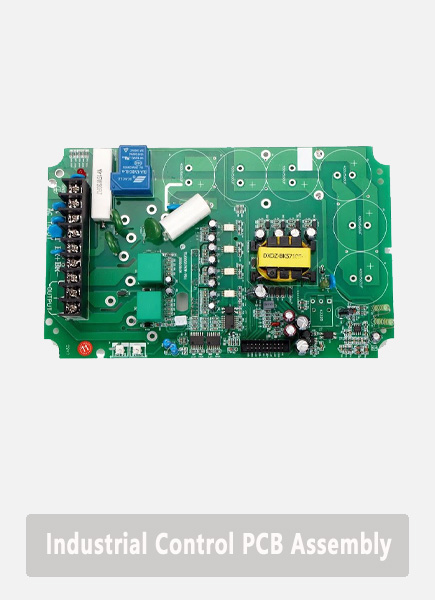
After prototype approval, we can support repeat production and batch manufacturing. This helps customers reduce quality variation from first trial order to long-term supply. - PCB assembly and component sourcing
We provide component sourcing and PCB assembly support. Customers can reduce the time spent coordinating PCB fabrication, components, and SMT assembly separately. - More PCB technology options
EBest PCB supports FR4 PCB, multilayer PCB, metal core PCB, ceramic PCB, flexible PCB, rigid-flex PCB, RF PCB, high TG PCB, heavy copper PCB, HDI PCB, high-speed PCB, and impedance control PCB. If a two-layer design is not enough, customers can choose a better PCB structure early. - Quality and compliance support
EBest PCB has IATF 16949, ISO 9001:2015, ISO 13485:2016, AS9100D, REACH, RoHS, and UL certifications. This helps overseas customers manage supplier evaluation, compliance requirements, and long-term production risk. - China source factory with global supply
Customers can work directly with a China PCB and PCBA source factory for custom production, prototype builds, batch orders, assembly support, and global delivery coordination. This helps reduce communication cost and supports global project delivery without false overseas factory claims.
FAQs About 2 Layer PCB Ground Plane
Q1: Can this ground structure be used for power circuits?
A1: Yes, but the current path must be reviewed carefully. Power circuits should use wide copper, short return paths, enough vias, and proper copper thickness. If the board has high current, heat, or switching noise, the layout should be checked before production.
Q2: Is a full bottom ground plane always possible on a two-layer PCB?
A2: Not always. Dense routing, connectors, vias, and component placement may cut the bottom copper. The goal is to keep the main ground area as continuous as possible and avoid long traces that divide the return path.
Q3: What is the biggest mistake in two-layer PCB grounding?
A3: The biggest mistake is treating copper pour as a real ground plane without checking continuity. A copper area with narrow necks, isolated islands, or broken return paths may pass DRC but still create noise, EMI, and unstable signals.
Q4: Should digital ground and analog ground be separated on a two-layer PCB?
A4: Usually, one continuous ground plane is safer. Instead of splitting ground, separate analog and digital circuits by placement. Keep sensors, ADC inputs, and references away from switching regulators, clocks, motors, and high-current loads.
Q5: How close should bypass caps be to IC power pins?
A5: They should be placed as close as practical to the power pins. The power pin, capacitor, and ground connection should form a small current loop. Long ground traces reduce decoupling performance and may cause power noise.
Q6: Can a 2 layer PCB support USB or other high-speed signals?
A6: It can support simple short high-speed traces if the ground reference is continuous and routing is clean. For strict impedance, longer routing, dense layout, or EMI-sensitive products, 4 layers is usually a better choice.
Q7: Why does a two-layer PCB fail EMI testing?
A7: Common reasons include broken ground planes, large current loops, poor capacitor grounding, long clock traces, noisy switching regulators, and cable-connected signals without proper filtering. EMI risk should be reviewed before Gerber output.
Q8: Are stitching vias necessary for two-layer PCB grounding?
A8: They are strongly recommended when both layers have ground copper. Stitching vias connect top and bottom ground areas, reduce impedance, and help control noise near connectors, board edges, regulators, and separated copper regions.
Q9: What copper thickness should be used for a 2 layer PCB?
A9: Many standard two-layer boards use 1 oz copper. Higher current boards may use 2 oz or thicker copper, depending on trace width, temperature rise, board size, and assembly needs. Current should be reviewed before manufacturing.
Q10: When should a buyer upgrade from 2 layer PCB to 4 layer PCB?
A10: Upgrade when the design has high-speed signals, RF circuits, dense components, strict EMI requirements, multiple power rails, or sensitive analog measurement. If redesign risk is high, 4 layers may reduce total project cost.
Q11: Can ground pour reduce PCB temperature?
A11: Ground copper can help spread heat, especially near regulators, LEDs, MOSFETs, and connectors. However, thermal performance depends on copper area, copper thickness, vias, component placement, and the heat path to the enclosure or airflow.
Q12: What should be sent to EBest PCB for review and quotation?
A12: Send Gerber files, drill files, BOM, assembly drawings, quantity, copper thickness, surface finish, and special requirements. If the board has high current, EMI risk, or high-speed routing, also share the key circuit function.
Conclusion
A reliable 2 layer PCB ground plane depends on continuous copper, short return paths, correct bypass cap placement, clean routing, and careful review before manufacturing. For simple and cost-sensitive circuits, a two-layer PCB can work well. For high-speed, dense, EMI-sensitive, or mixed-signal products, a 4 layer PCB should be evaluated early.
EBest Circuit can support 2 layer PCB fabrication, DFM review, copper thickness evaluation, PCB assembly, component sourcing, prototype builds, and mass production from our China source factory. Send your Gerber files, BOM, quantity, and technical requirements to sales@bestpcbs.com for a fast quotation.