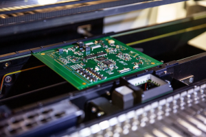
When engineers search for quick turn PCB USA, they are usually looking for more than a short production time. They need fast engineering response, reliable PCB fabrication, clear communication, complete assembly support, and delivery that can keep a U.S. hardware project moving. For prototype development, product validation, customer demos, engineering fixes, or small-batch production, lead time can directly affect product launch schedules.
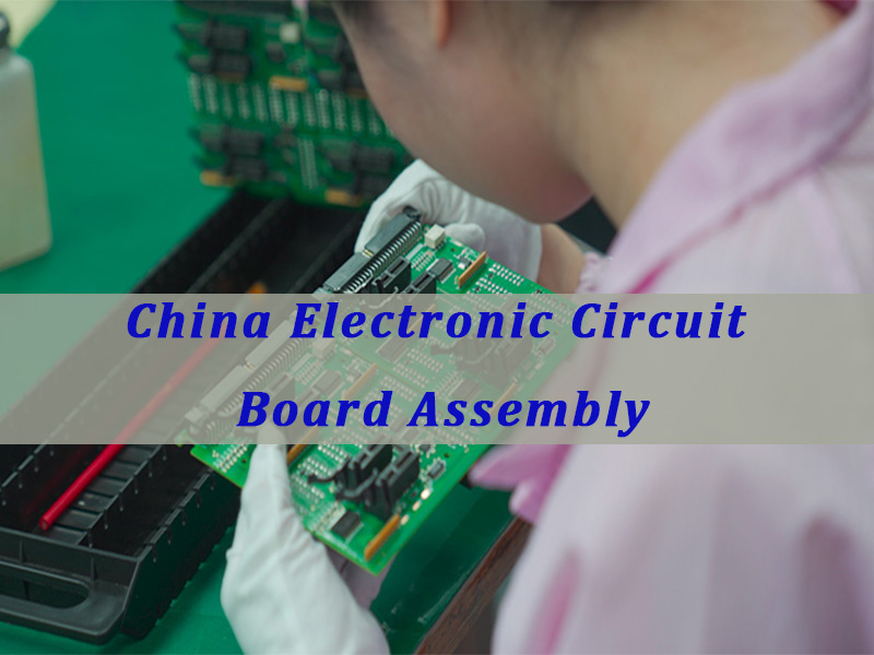
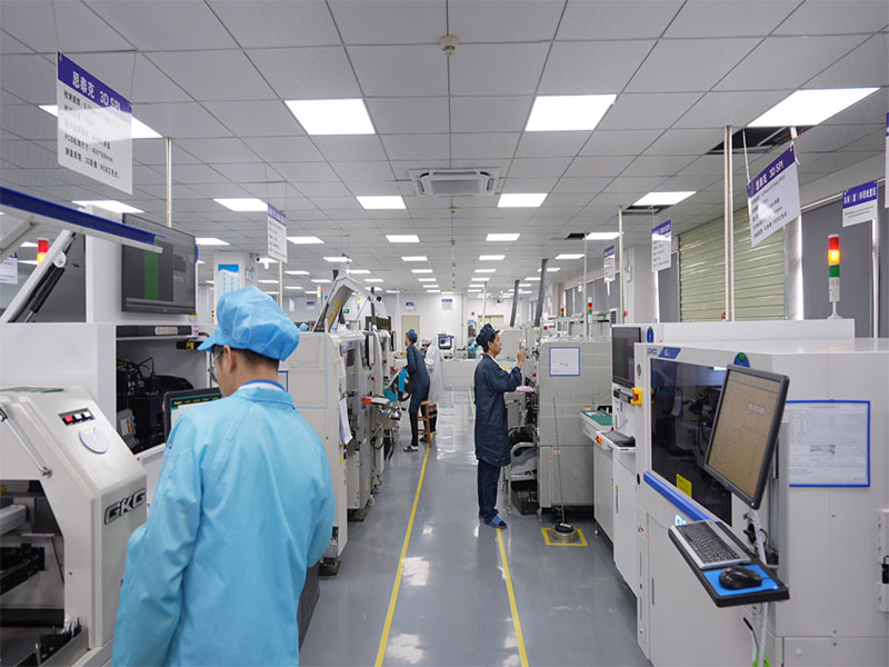
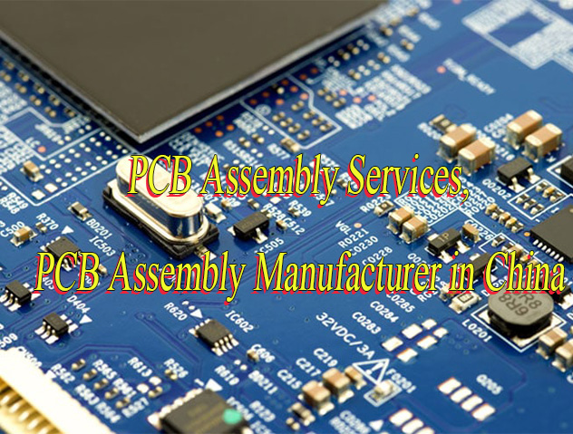
EBest Circuit, also known as Best Technology, is a China-based PCB and PCBA manufacturer supporting U.S. customers with quick turn PCB fabrication, PCB prototype, SMT assembly, and full or partial turnkey PCBA services. Although we are not located in the USA, we support fast response, engineering review, urgent PCB production, PCBA assembly, and door-to-door delivery to customer offices, factories, and laboratories in the United States. For quick turn PCB USA project support, please send your Gerber files, BOM, Pick-and-Place file, and assembly requirements to sales@bestpcbs.com.
What Is Quick Turn PCB USA?
Quick turn PCB USA usually refers to PCB fabrication or PCB assembly projects that must be completed faster than normal production schedules and delivered to customers in the United States. For many buyers, the real requirement is not only “made in the USA.” It is fast quotation, quick engineering review, stable manufacturing, assembly readiness, and reliable delivery to the U.S. market.
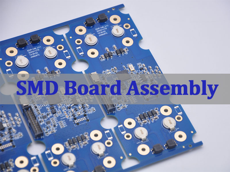
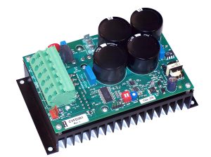
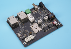
At EBest Circuit, we support U.S. customers with quick turn PCB and PCBA projects from China. Our quick turn support can include PCB prototype production, FR4 PCB, MCPCB, ceramic PCB, HDI PCB, heavy copper PCB, high TG PCB, RF PCB, rigid-flex PCB, SMT assembly, THT assembly, mixed assembly, and turnkey or partial turnkey PCBA.
For U.S. customers, quick turn PCB projects are commonly used for engineering validation, prototype testing, EVT and DVT builds, customer demo samples, urgent board replacement, small-batch pilot production, design verification before mass production, and PCB assembly samples before full production.
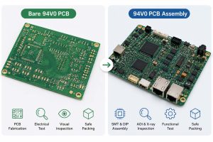
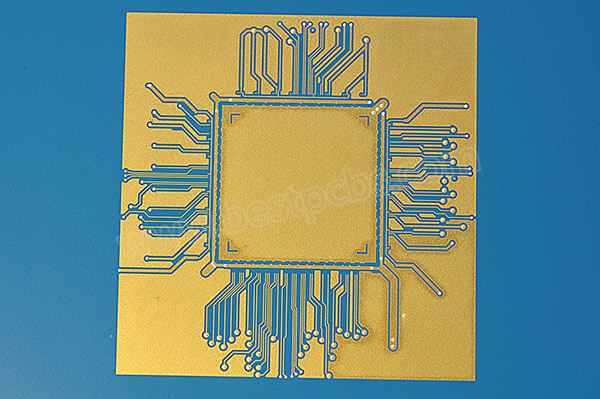
A quick turn project still follows the normal PCB manufacturing process. Even one prototype board must go through engineering review, material preparation, drilling, imaging, etching, solder mask, surface finish, electrical testing, inspection, and packaging. This is why quick turn PCB is not only about speed; it also depends on whether the design is ready for manufacturing.
What Types of PCBs Are Suitable for Quick Turn Production?
EBest Circuit supports quick turn PCB projects for different board types, but not every PCB has the same fast-turn feasibility. Standard FR4 prototypes are usually the fastest. Special materials, higher layer counts, HDI structures, rigid-flex stack-ups, ceramic substrates, and heavy copper designs need more engineering review before lead time can be confirmed.
| PCB Type | Quick Turn Fit | Key Lead Time Factor |
|---|---|---|
| FR4 PCB | High | Layer count and standard specs |
| MCPCB | High for simple 1L | Aluminum thickness and copper weight |
| High TG PCB | Medium | Material availability |
| HDI PCB | Case by case | Via structure and lamination |
| Heavy Copper PCB | Case by case | Copper thickness |
| RF PCB | Case by case | RF laminate and impedance |
| Rigid-Flex PCB | Case by case | Stack-up and bend area |
| Ceramic PCB | Longer lead time | Substrate and process |
| PCBA | Fast if parts ready | BOM and component supply |
For urgent projects, EBest Circuit first checks whether the design matches standard quick turn conditions. If the board needs special materials, tight tolerances, controlled impedance, via-in-pad, thick copper, or advanced assembly, our team will confirm a practical lead time before production.
Quick Turn PCB USA Lead Time: Bare Board vs PCB Assembly
EBest Circuit provides both normal delivery and fast service. Urgent boards can be shipped out within 24 hours for suitable projects. Unless otherwise specified, quoted prices are usually based on normal delivery. For urgent orders, customers should clearly mention the required delivery date by email, so we can evaluate fast production and priority scheduling.
FR4 Prototype Lead Time
For standard FR4 prototypes under 1 square meter:
| Layers | Normal | Fastest |
|---|---|---|
| 1L | 7 days | 24H |
| 2L | 8 days | 24H |
| 4L | 10 days | 48H |
| 6L | 10 days | 72H |
| 8L | 12 days | 72H |
| 10L+ | TBD | TBD |
Standard FR4 quick turn conditions usually include 0.4–1.6mm thickness, H/H or 1oz copper, lead-free HASL, green solder mask, white silkscreen, line width/space above 8 mil, hole size above 0.3mm, and annular ring above 10 mil.
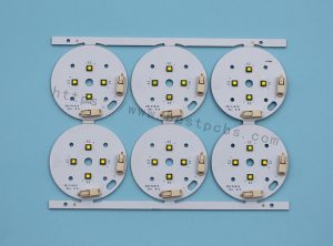
MCPCB Prototype Lead Time
For standard MCPCB prototypes under 1 square meter:
| Layers | Normal | Fastest |
|---|---|---|
| 1L | 4 days | 24H |
| 2L | 14 days | 168H |
| 4L | 21 days | TBD |
Standard MCPCB conditions usually include aluminum substrate, 0.8–2.0mm thickness, H/H or 2oz copper, lead-free HASL, white solder mask, black silkscreen, and thermal conductivity around 0.8W/m·K.
Other PCB and PCBA Lead Time
| Item | Normal | Fastest |
|---|---|---|
| Rigid-flex PCB | 2 weeks for 4L | 1.5 weeks |
| Ceramic PCB | 3 weeks | 2 weeks |
| PCBA | 1 week | 2 days |
Actual lead time depends on design complexity, material availability, production load, component supply, testing requirements, and engineering confirmation. For urgent U.S. projects, it is better to send Gerber files, BOM, Pick-and-Place file, assembly drawing, and delivery target at the same time.
What Files Are Needed for Quick Turn PCB Assembly Services USA?
Quick turn PCB assembly services USA require complete files from the beginning. Missing BOM data, unclear Pick-and-Place files, or incomplete assembly notes can delay even a simple order.
| File | Purpose |
|---|---|
| Gerber / ODB++ | PCB fabrication |
| Stack-up | Layer and impedance review |
| Fab drawing | Dimensions, holes, finish, tolerances |
| BOM | Component sourcing |
| MPNs | Accurate part matching |
| Substitutes | Faster sourcing |
| Pick-and-Place | SMT programming |
| Assembly drawing | Polarity and placement check |
| Test requirements | Inspection and function test |
| Panel drawing | SMT and delivery format |
For faster review, the BOM should include MPNs, package, quantity, reference designators, and DNI parts. For PCBA, please also provide polarity notes for ICs, diodes, LEDs, electrolytic capacitors, connectors, BGA, and fine-pitch components.
EBest Circuit PCBA Capability
| Item | Capability |
|---|---|
| Assembly | SMT, THT, mixed |
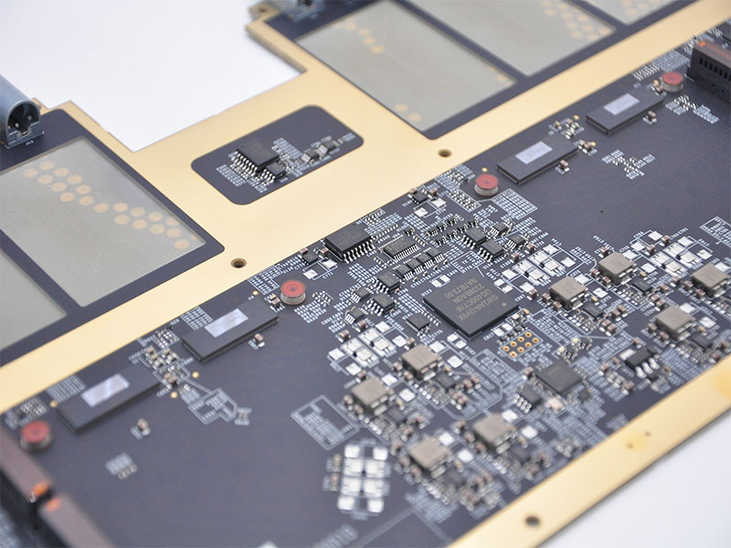
| Min SMD | 01005 |
| Min BGA pitch | 0.25mm |
| Board size | 0.2 × 0.2 in to 20 × 20 in / 22 × 47.5 in |
| Component format | Reel, cut tape, tube, tray, loose parts |
| Capacity | 13,200,000 chips/day |
| Lead time | 1–5 days |
| Inspection | AOI, X-ray |
| Testing | Functional test |
| Extra process | Wave soldering, hand soldering, coating, box build |
EBest Circuit supports SMT assembly, THT assembly, mixed assembly, BGA assembly, AOI inspection, X-ray inspection, functional testing, DIP / THT assembly, wave soldering, hand soldering, conformal coating, and box build assembly. For urgent PCBA projects, component availability is often the main schedule factor.
What Factors Can Delay a Quick Turn PCB Order?
Most quick turn delays come from file issues, unclear requirements, special processes, or component availability. EBest Circuit checks these risks before production so U.S. customers can avoid unnecessary waiting time.
| Delay Factor | Main Risk | How to Avoid |
|---|---|---|
| Missing Gerber | Cannot release production | Send complete files |
| Unclear fab notes | Wrong specs risk | Confirm finish, copper, tolerance |
| Incomplete BOM | Sourcing delay | Add MPNs and quantities |
| No PnP file | SMT delay | Provide centroid file |
| Missing polarity | Assembly risk | Mark Pin 1 and polarity |
| Special material | Longer sourcing | Confirm before quote |
| HDI structure | More lamination | Confirm stack-up |
| Via-in-pad | Extra process | Mark clearly |
| Thick copper | Longer plating/etching | Confirm copper weight |
| ENIG + hard gold | Extra finish process | Confirm finish early |
| Part shortage | SMT cannot start | Add substitutes |
| Late reply | EQ not closed | Respond quickly |
| Weekend/holiday | Schedule shift | Plan business days |
| GMT+8 cut-off | Time-zone delay | Submit before 17:00 GMT+8 |
The fastest quick turn results usually come from complete files, standard materials, available components, and quick engineering confirmation. If our engineering team has to ask for missing BOM data, unclear stack-up, wrong PnP rotation, or incomplete panel information, the lead time will be affected even if the factory has fast production capacity.
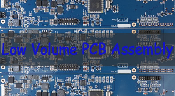
Full Turnkey, Partial Turnkey, or Consigned Assembly: Which Is Faster?
Assembly mode affects quick turn PCB USA lead time. The fastest option depends on whether parts are available, whether the customer has controlled components, and whether the kitting information is accurate.
At EBest Circuit, we support flexible PCBA models for U.S. customers.
| Model | Best For | Speed Risk |
|---|---|---|
| Full turnkey | One-stop PCBA | Part availability |
| Partial turnkey | Customer-supplied key ICs | Customer parts arrival |
| Consigned | Customer has all parts | Kitting errors |
| Hybrid | Hard-to-source BOMs | Coordination |
For many U.S. prototype projects, full turnkey PCB assembly is the easiest option because EBest Circuit manages PCB fabrication, component sourcing, SMT stencil, SMT assembly, inspection, and shipment. Partial turnkey can be faster when the customer already has key ICs or locked AVL parts.
The fastest assembly route is usually not decided by the assembly model alone. It depends on whether the files are complete, the parts are available, the stencil can be prepared in parallel, and the engineering questions are answered quickly.
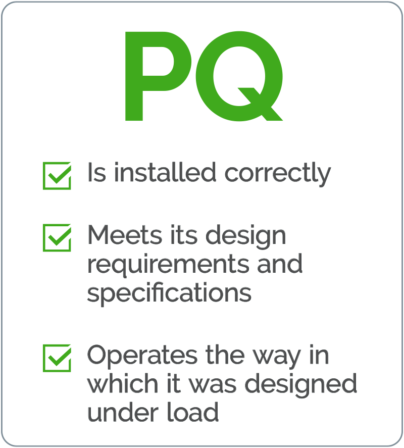
How to Pass DFM and DFT Checks Before Quick Turn Production?
DFM and DFT checks are important for quick turn PCB USA projects because they help prevent design issues from entering production. A fast schedule does not mean the engineering review should be skipped. If the board has manufacturability problems, skipping DFM can lead to scrap, rework, or assembly failure.
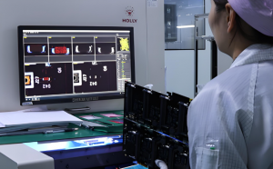
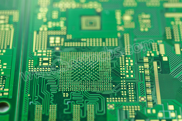
EBest Circuit reviews quick turn projects before production to reduce these risks. For PCB fabrication, we check board size, layer count, stack-up, line width and spacing, hole size, annular ring, copper thickness, solder mask clearance, surface finish, impedance requirement, panelization, and special process notes.
For PCBA, we check BOM clarity, component package, polarity, Pick-and-Place data, fiducial marks, stencil requirement, BGA assembly needs, inspection method, and functional test requirements.
Before sending a quick turn order, U.S. customers should check:
- Are all Gerber layers complete?
- Is the board outline clear?
- Is the stack-up confirmed?
- Are copper thickness and surface finish specified?
- Are impedance requirements listed?
- Are all drill files included?
- Is the BOM complete with MPNs?
- Are substitute parts allowed?
- Are all polarized components marked?
- Is the Pick-and-Place file aligned with the Gerber origin?
- Are BGA and fine-pitch components clearly identified?
- Are test requirements available?
- Is panelization needed for SMT?
- Is the delivery address confirmed?
DFT is especially important when the assembled board must pass functional testing. If the customer needs programming, fixture testing, ICT, or functional test, the test method should be discussed before production. This allows the factory to prepare inspection and test flow early instead of waiting until after SMT assembly.
Top 10 Quick Turn PCB USA Suppliers to Compare
For buyers searching quick turn PCB USA, it is helpful to compare several suppliers before placing an urgent order. This list is not a fixed ranking. It is a practical supplier comparison list for buyers who want to evaluate lead time, PCB capability, assembly support, engineering review, quality control, communication speed, and delivery options.
| Supplier | Main Focus |
|---|---|
| Sierra Circuits | Quick-turn PCB and assembly |
| AdvancedPCB | Rapid prototype PCB |
| Sunstone Circuits | PCBExpress quickturn boards |
| Bay Area Circuits | Prototype and turnkey support |
| PCB Unlimited | USA quickturn PCB |
| MacroFab | North American PCBA platform |
| Screaming Circuits | Quick-turn PCBA |
| Epec Engineered Technologies | Rigid, flex, rigid-flex quick turns |
| RUSH PCB | Quick-turn fabrication and assembly |
| FastTurn PCBs | Fast PCB and turnkey PCBA |
As a reliable 24 hour pcb manufacturer, EBest Circuit can also be considered by U.S. customers who are open to working with a China-based PCB and PCBA manufacturer for quick turn projects. The key difference is that EBest Circuit does not position itself as a USA-based factory. Instead, we support U.S. customers through fast engineering communication, quick PCB prototype production, SMT assembly, full or partial turnkey PCBA, and door-to-door delivery to the United States.
When comparing suppliers, buyers should avoid choosing only by the shortest advertised lead time. A realistic quick turn PCB supplier should also explain what specifications qualify for fast service, what files are required, how engineering questions are handled, what assembly options are available, and how urgent shipment is arranged.
How to Choose a Quick Turn PCB Manufacturer USA?
When U.S. customers look for a quick turn PCB manufacturer USA, the first question is often location. Local manufacturing can be useful for certain urgent, regulated, or ITAR-sensitive projects. However, location is not the only factor. Many commercial projects also require fast engineering response, clear DFM review, competitive prototype cost, flexible PCBA support, and reliable international delivery.
| Buyer Concern | What to Check |
|---|---|
| Lead time | Standard vs urgent options |
| PCB capability | FR4, MCPCB, ceramic, HDI, heavy copper |
| PCBA support | SMT, THT, BGA, AOI, X-ray |
| Sourcing | Turnkey, partial turnkey, consigned |
| Engineering | DFM and DFT review |
| Quality | Inspection and testing |
| Delivery | DHL, FedEx, UPS, TNT, air freight |
| Compliance | ISO, UL, RoHS, REACH |
| Communication | Fast EQ response |
EBest Circuit supports DHL, FedEx, UPS, TNT, air freight, and door-to-door delivery. Finished PCB and PCBA orders can be shipped directly to customer offices, factories, laboratories, or assembly partners in the United States.
For customers in industrial, medical, automotive, aerospace, and electronic product development, EBest Circuit supports projects with quality systems and compliance references such as ISO9001, ISO13485, IATF16949, AS9100D, UL, RoHS, REACH, and SGS.
Real-World Quick Turn PCB USA Project Support from EBest Circuit
A real quick turn PCB USA project is not only about producing boards fast. It also requires file review, material preparation, component sourcing, SMT planning, inspection, and shipment coordination.
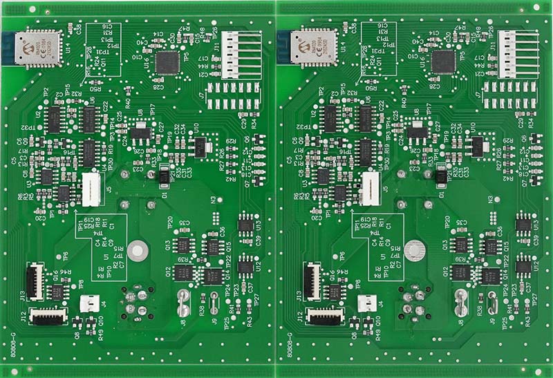
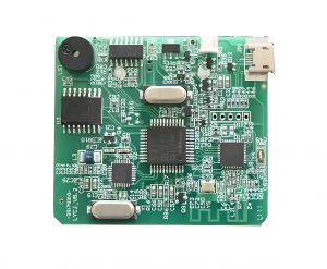
One typical project supported by EBest Circuit was a single-sided FR4 PCB assembly project for a U.S. customer.
| Project Item | Details |
|---|---|
| Board type | Single-sided FR4 |
| Thickness | 1.57mm |
| Copper | 2oz |
| Solder mask | Green |
| Silkscreen | White |
| Surface finish | Lead-free HASL |
| Delivery format | 10-up panel |
| Assembly | SMT |
| Components | Purchased by EBest Circuit |
EBest Circuit supported this project with Gerber review, DFM check, PCB fabrication, panel confirmation, stencil preparation, component sourcing, SMT assembly, AOI inspection, and shipment arrangement.
The key to speed was not only PCB fabrication. The project also needed complete Gerber data, clear BOM, accurate Pick-and-Place file, confirmed panel delivery format, available components, and fast engineering confirmation. By managing PCB production and SMT assembly together, EBest Circuit helped reduce communication gaps between separate PCB and assembly suppliers.
This type of project is common for U.S. customers who need prototype verification, pilot build preparation, or urgent assembled boards for testing. When the board design is simple but the project includes SMT assembly and component sourcing, a one-stop PCB and PCBA supplier can often save coordination time.
EBest Circuit also supports other quick turn project scenarios, such as FR4 prototype boards for engineering validation, MCPCB prototypes for LED and thermal applications, ceramic PCB samples for high-power electronics, rigid-flex prototypes for compact devices, and partial turnkey PCBA when customers supply key ICs and we source the remaining parts.
Why Choose EBest Circuit (Best Technology) for Quick Turn PCB USA Projects?
EBest Circuit is a China-based PCB and PCBA manufacturer supporting U.S. customers with quick turn PCB fabrication, prototype PCB assembly, and full or partial turnkey PCBA. We are not a USA-based factory, but we support U.S. customers with engineering review, fast production options, flexible assembly service, quality inspection, and door-to-door delivery.
| Customer Need | EBest Circuit Support |
|---|---|
| PCB prototype | FR4, MCPCB, ceramic, HDI, heavy copper |
| Urgent boards | Fast service for suitable designs |
| PCBA | SMT, THT, BGA, mixed assembly |
| Turnkey service | Full, partial, consigned, hybrid |
| Engineering | DFM and DFT review |
| Sourcing | BOM review and component purchasing |
| Inspection | AOI, X-ray, functional test |
| U.S. delivery | DHL, FedEx, UPS, TNT, air freight |
| Quality system | ISO9001, ISO13485, IATF16949, AS9100D, UL, RoHS, REACH, SGS |
For urgent projects, customers should send the required delivery date, target application, quantity, board type, assembly requirement, and shipment address at the beginning. This helps our team choose a practical production route before manufacturing.
The best quick turn result comes from clear communication. If the files are complete, materials are available, components can be sourced quickly, and engineering questions are confirmed early, EBest Circuit can help U.S. customers move from design files to finished PCB or PCBA faster and with fewer risks.
FAQs About Quick Turn PCB USA
Q1: Is EBest Circuit a USA-based quick turn PCB manufacturer?
A1: No. EBest Circuit, also known as Best Technology, is a China-based PCB and PCBA manufacturer. We support U.S. customers with quick turn PCB fabrication, PCB prototype, SMT assembly, turnkey PCBA, partial turnkey PCBA, and door-to-door delivery to the United States.
Q2: Can EBest Circuit ship quick turn PCB orders to the USA?
A2: Yes. We support DHL, FedEx, UPS, TNT, air freight, and door-to-door delivery. Finished PCB and PCBA orders can be shipped to U.S. customer offices, factories, laboratories, or assembly partners.
Q3: What is the fastest lead time for FR4 prototype PCB?
A3: For suitable standard FR4 prototype projects under 1 square meter, the fastest service can be 24 hours for 1-layer and 2-layer boards, 48 hours for 4-layer boards, and 72 hours for 6-layer and 8-layer boards. Actual lead time depends on design complexity, file completeness, production load, and order confirmation time.
Q4: Can quick turn PCB also include assembly?
A4: Yes. EBest Circuit supports quick turn PCBA projects, including SMT assembly, THT assembly, mixed assembly, BGA assembly, AOI inspection, X-ray inspection, functional testing, conformal coating, and box build assembly. PCBA lead time can be 1–5 days depending on project requirements.
Q5: What files should I send for quick turn PCB assembly?
A5: For PCB assembly, please send Gerber or ODB++ files, BOM, Pick-and-Place file, assembly drawing, test requirements, and any special manufacturing notes. For faster review, the BOM should include manufacturer part numbers, packages, quantities, reference designators, and acceptable substitutes.
Q6: Which assembly model is best for urgent PCBA?
A6: It depends on component availability. Full turnkey is convenient when all parts can be sourced quickly. Partial turnkey is useful when the customer supplies key ICs or controlled parts. Consigned assembly can be fast if all customer-supplied components arrive correctly packed and on time.
Q7: Can EBest Circuit support BGA and fine-pitch assembly?
A7: Yes. We support BGA assembly, X-ray inspection, AOI inspection, and fine-pitch SMT assembly. Our PCBA capability includes 01005 minimum SMD components and 0.25mm minimum BGA pitch.
Q8: What usually delays a quick turn PCB USA order?
A8: Common delays include missing Gerber layers, unclear BOM, no Pick-and-Place file, missing polarity notes, special materials, component shortage, HDI stack-up complexity, via-in-pad, thick copper, special surface finishes, late engineering replies, holidays, and time-zone differences.
Q9: Can EBest Circuit support full turnkey and partial turnkey PCBA for U.S. customers?
A9: Yes. We support full turnkey PCBA, partial turnkey PCBA, consigned assembly, and hybrid sourcing models. Customers can ask us to source all components, supply key parts themselves, or divide sourcing based on urgency and BOM risk.
Q10: How can I start a quick turn PCB USA project with EBest Circuit?
A10: Send your Gerber files, BOM, Pick-and-Place file, assembly drawing, quantity, board type, delivery target, and shipment address to sales@bestpcbs.com. Our team will review your files and help confirm a practical production route.
To sum up, quick turn PCB USA projects require more than a short advertised lead time. For U.S. customers, the real value comes from fast engineering response, complete file review, realistic scheduling, stable PCB fabrication, PCBA assembly capability, component sourcing support, inspection, and reliable delivery.
EBest Circuit supports U.S. customers as a China-based PCB and PCBA manufacturer with quick turn PCB fabrication, PCB prototype, MCPCB, ceramic PCB, rigid-flex PCB, and full / partial turnkey PCBA services. If you need quick turn PCB fabrication, PCB prototype, MCPCB, ceramic PCB, rigid-flex PCB, or full / partial turnkey PCBA support for the U.S. market, send your Gerber files, BOM, Pick-and-Place file, test requirements, and delivery schedule to sales@bestpcbs.com. Our team will help you choose a practical production route based on board type, urgency, component availability, and assembly requirements.