PCB manufacturing PCB manufacturing
Home > Blog

GPU PCB

GPU PCB Design and Manufacturing Guide: Components, Materials, Layers, and Assembly
Tuesday, July 7th, 2026

What Is a GPU PCB?

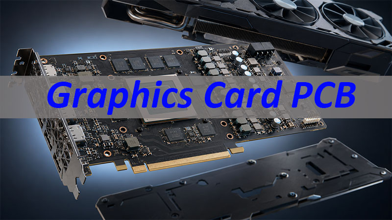
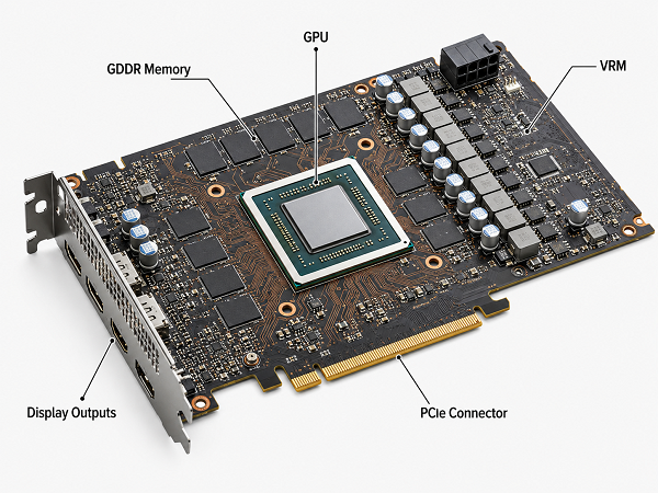
A GPU PCB is the printed circuit board that supports and connects the graphics processing unit, memory chips, power circuits, connectors, and control components in a graphics card or GPU-based computing module. It is not only a carrier for the GPU package. It is also the electrical and thermal platform that allows high-speed signals, high current power delivery, and stable heat transfer to work together.

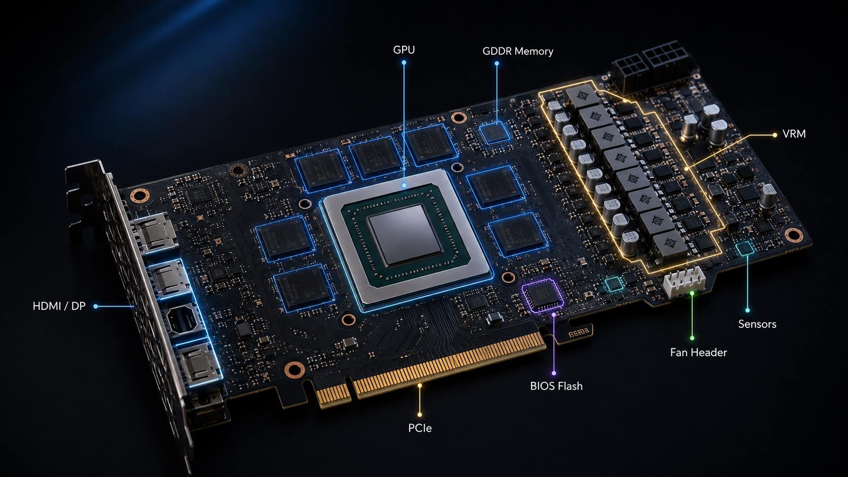
In a typical graphics card, the GPU sits near the center of the board, surrounded by GDDR memory, VRM power stages, decoupling capacitors, clock circuits, display interfaces, and PCIe edge fingers. In AI accelerators or industrial GPU modules, the structure may be more customized, but the core design logic remains similar: stable power, controlled impedance, short high-speed paths, and reliable heat management.
What Is a GPU PCB?

What is a GPU PCB Made of?

A GPU PCB is made of insulating laminate, copper foil, plated vias, solder mask, surface finish, and assembled electronic components. The exact structure depends on performance level, board size, memory interface, power load, and cooling design.

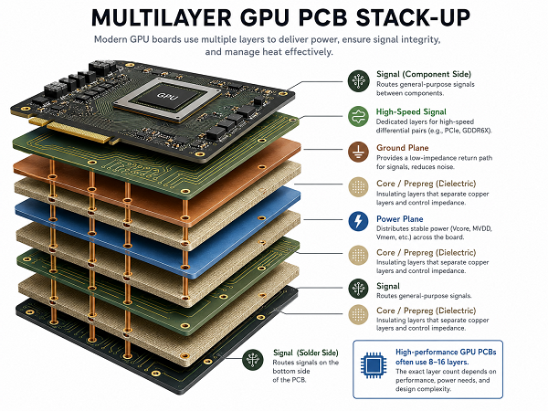
The base material is usually high Tg FR4 or a higher-performance low-loss laminate. Copper layers form signal routing, power planes, and ground planes. Prepreg and core materials separate the copper layers and control dielectric thickness. Plated through holes, blind vias, buried vias, and sometimes microvias connect different layers.

What Are the Key Components on a GPU PCB?

A GPU PCB contains both high-speed digital circuits and high-current power circuits. These two areas have very different design requirements, so component placement must be planned carefully from the beginning.

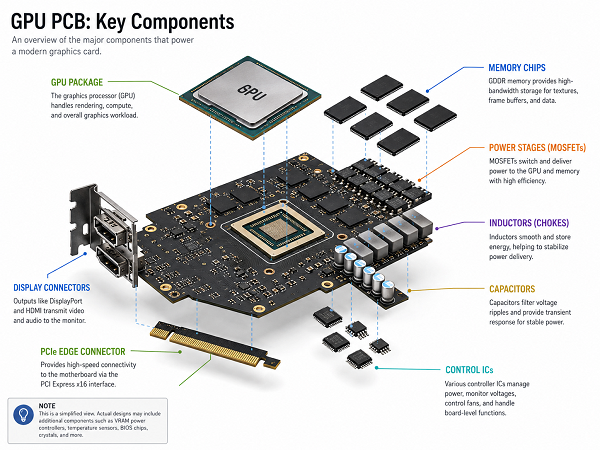
Key GPU PCB components usually include:

ComponentMain RoleDesign Concern
GPU packageMain graphics or parallel computing processorFine-pitch BGA routing, power delivery, thermal path
GDDR memoryHigh-speed graphics memoryLength matching, impedance control, clean reference planes
VRM controllerControls GPU and memory power phasesFeedback routing, phase balance, noise control
MOSFETs / power stagesSwitch high current for core and memory railsHeat, current loop size, copper area
InductorsStore energy in buck converter stagesPlacement, current rating, magnetic field control
MLCC capacitorsLocal decoupling and noise suppressionLow inductance placement near GPU and memory
Bulk capacitorsHandle lower-frequency load changesRipple current, voltage rating, temperature rating
PCIe edge connectorConnects the card to the motherboardControlled impedance, plating quality, mechanical accuracy
Display connectorsHDMI, DisplayPort, or other outputsESD protection, differential pair routing
Clock componentsProvide reference timingJitter control, isolation from noisy power areas
Sensors and protection ICsMonitor temperature, voltage, and currentAccurate placement and clean signal routing
What Are the Key Components on a GPU PCB?

How Many Layers Does a GPU PCB Need?

Most GPU PCBs use multilayer structures because they need dense BGA fanout, high-speed memory routing, PCIe routing, stable power planes, and continuous ground reference layers. A simple low-power GPU board may use 8 to 10 layers, while high-performance graphics cards and AI accelerator boards often require 12, 14, 16, or more layers.

Layer count should be selected by routing density and electrical performance, not by appearance or cost alone.

GPU PCB TypeCommon Layer RangeSuitable Use
Low-power GPU module6–8 layersEmbedded graphics, compact industrial display systems
Mid-range graphics card8–12 layersConsumer or industrial GPU applications
High-performance graphics card12–16 layersHigh-speed memory, stronger VRM, tighter SI/PI needs
AI accelerator / HPC board16–24+ layersDense BGA, high current, PCIe high-speed links, complex power rails

A higher layer count is useful when it allows cleaner routing, better return paths, wider power planes, and more stable impedance. It becomes unnecessary when the added layers do not reduce risk or improve manufacturability.
How Many Layers Does a GPU PCB Need?

What Materials Are Used for GPU PCB Manufacturing?

GPU PCB manufacturing commonly uses high Tg FR4, low-loss FR4, halogen-free laminate, or advanced high-speed materials. Material selection depends on operating temperature, signal speed, board thickness, layer count, and cost target.

Material TypeTypical UseStrengthLimitation
Standard FR4Low-cost, lower-speed boardsEasy to source and fabricateLimited thermal and high-speed performance
High Tg FR4Multilayer GPU PCBs with higher thermal demandBetter heat resistance and dimensional stabilityStill not ideal for very high-speed or low-loss designs
Low-loss FR4PCIe and high-speed memory routingLower signal loss than standard FR4Higher material cost
Halogen-free laminateProducts with environmental or customer requirementsBetter compliance positioningMaterial availability should be confirmed early
Hybrid stack-upCost-sensitive high-speed boardsUses premium material only where neededRequires careful lamination and stack-up control

Standard FR4 may be acceptable for low-speed control areas, but high-speed memory and PCIe channels often need tighter dielectric control and lower signal loss. For high-power GPUs, thermal stability and resin reliability are also important because the board may operate near hot components for long periods.

Why Does a GPU PCB Need High-Speed Signal Control?

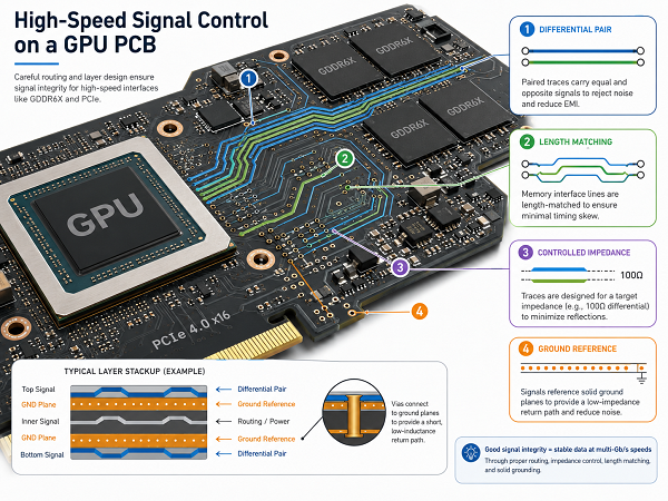
A GPU PCB needs high-speed signal control because PCIe lanes, memory buses, clocks, and display interfaces operate at high data rates. At these speeds, traces behave as transmission lines. Trace width, spacing, dielectric thickness, copper roughness, via stubs, return path changes, and connector transitions can all affect signal quality.

Important high-speed control points include:

  • Keep differential pairs tightly controlled for width, spacing, and reference plane continuity.
  • Avoid unnecessary layer transitions on critical channels.
  • Use ground vias near signal vias when changing layers.
  • Keep memory routing short, matched, and referenced to solid planes.
  • Avoid routing high-speed lines across plane splits.
  • Confirm impedance with the manufacturer before fabrication.
  • Use back drilling or optimized via structures when via stubs become a signal risk.
Why Does a GPU PCB Need High-Speed Signal Control?

Why Is VRM Layout Important in GPU PCB Design?

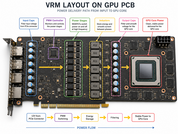
VRM layout is critical because the GPU core needs high current at low voltage. Even a small layout problem in the voltage regulator module can cause voltage ripple, heat concentration, switching noise, or unstable operation during load changes.

A GPU VRM usually includes a PWM controller, driver or power stage, MOSFETs, inductors, input capacitors, output capacitors, current sensing circuits, and feedback routing. The highest-risk area is the switching power loop. This loop should be compact, direct, and supported by enough copper. Long loops increase parasitic inductance, which can create ringing, EMI, and extra heat.

Good VRM layout should consider:

  • Place input capacitors close to power stages.
  • Keep switching nodes compact and away from sensitive signals.
  • Use wide copper and multiple vias for high-current paths.
  • Separate noisy switching areas from clock, memory, and feedback traces.
  • Place output capacitors close to GPU power pins when possible.
  • Use solid ground reference and short return paths.
  • Balance phase layout to avoid uneven thermal loading.

Heavy copper may be useful in VRM and power regions, but it is not always suitable for the entire board. Thick copper increases etching difficulty and may affect fine-line routing.
Why Is VRM Layout Important in GPU PCB Design?

How Do Manufacturers Manage Heat in GPU PCBs?

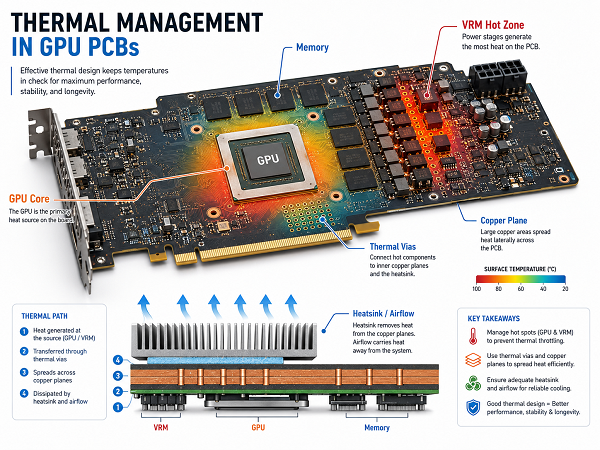
GPU PCBs generate heat from several areas, including the GPU core, VRAM, VRM power stages, and high-current traces. While the main cooling system usually includes a heatsink, fan, thermal pads, or enclosure-level thermal design, the PCB still plays an important role in heat spreading. Copper planes can help distribute heat across the board. Thermal vias can move heat from one layer to another. High Tg materials can improve board stability under elevated temperatures.

In power areas, heavier copper may improve current handling and heat dissipation. Board thickness, copper distribution, component placement, and the connection between thermal pads and heatsinks should be reviewed together. In some high-power electronic modules, metal core or metal-backed PCB structures may be considered, but standard graphics card PCBs are usually based on multilayer FR4 or advanced high-speed laminates.
How Do Manufacturers Manage Heat in GPU PCBs?

What Should Engineers Consider During GPU PCB Assembly?

GPU PCB assembly requires careful handling because the board may include fine-pitch BGA packages, dense memory chips, large thermal pads, small passive components, and high-current power parts. The assembly process must support both precision placement and stable soldering.

Engineers should consider package type, component moisture sensitivity, solder paste selection, stencil design, reflow profile, X-ray inspection, and cleaning requirements. BGA components need accurate placement and controlled reflow. Power stages and large thermal pads may need special stencil aperture design to reduce voids. Small capacitors near the GPU require good placement accuracy because they directly affect decoupling performance.

For turnkey GPU PCB assembly, the quotation package should include:

  • Gerber files
  • BOM with manufacturer part numbers
  • Pick-and-place file
  • Assembly drawing
  • Stack-up and impedance requirements
  • PCB thickness and copper weight
  • Surface finish requirement
  • Test plan or functional test method
  • Any preferred component brands or approved substitutes
  • Packaging and reliability requirements

GPU PCB Design Guidelines

A reliable GPU PCB design starts with stack-up planning. The stack-up decides impedance, return path quality, power plane structure, dielectric spacing, and manufacturing difficulty.

Useful design guidelines include:

  • Define stack-up and impedance before routing.
  • Keep PCIe, GDDR, clock, and display lines on controlled layers.
  • Use solid ground reference under high-speed traces.
  • Keep decoupling capacitors close to GPU and memory power pins.
  • Keep VRM current loops short and wide.
  • Use enough vias for power and ground transitions.
  • Avoid routing sensitive signals near switching nodes.
  • Balance copper to reduce warpage.
  • Confirm minimum trace, spacing, via, and solder mask limits with the manufacturer.
  • Add test points for key voltage rails and control signals.

Avoid pushing every process limit in one design, fine lines, microvias, high layer count, heavy copper, and tight impedance tolerance are possible, but combining them increases cost and yield risk.

How Best Technology Supports GPU PCB and High-Performance PCB Projects

EBest Circuit, also known as Best Technology, supports GPU PCB and high-performance PCB projects through multilayer PCB fabrication, high Tg PCB, HDI PCB, heavy copper PCB, controlled impedance PCB, component sourcing, SMT assembly, BGA assembly, X-ray inspection, and turnkey PCBA service.

For GPU-related projects, the useful support usually starts before production. Customers can share Gerber files, BOM, stack-up, impedance table, PCB thickness, copper weight, and assembly requirements. The engineering team can then review material choice, layer structure, high-current areas, BGA fanout, solder mask clearance, and assembly risks before quotation or prototype build.

This is especially helpful for customers developing graphics cards, industrial GPU modules, AI accelerator boards, machine vision systems, edge computing devices, or high-performance embedded platforms. In these projects, the PCB is not just a purchased part. It directly affects signal quality, power stability, heat spreading, assembly yield, and long-term reliability.

FAQ

What is a GPU PCB?
A GPU PCB is the printed circuit board used in a graphics card or GPU module. It connects the GPU, memory, VRM, connectors, capacitors, sensors, and other electronic parts. It also supports high-speed signal routing, power delivery, and heat spreading.

How many layers does a GPU PCB usually have?
A GPU PCB usually has 8 to 16 layers, depending on performance level and routing density. Low-power GPU modules may use fewer layers, while high-end graphics cards or AI accelerator boards may need 16 layers or more.

What material is used for GPU PCB manufacturing?
GPU PCB manufacturing commonly uses high Tg FR4, low-loss FR4, halogen-free laminate, or hybrid material stack-ups. The right choice depends on signal speed, thermal demand, layer count, board thickness, and cost target.

Why does a GPU PCB need impedance control?
A GPU PCB needs impedance control because PCIe, memory, clock, and display signals operate at high speeds. Controlled impedance helps reduce signal reflections, timing problems, and unstable data transmission.

What is the role of VRM on a GPU PCB?
The VRM converts input power into stable low-voltage, high-current power for the GPU core and memory. A good VRM layout reduces voltage ripple, heat buildup, EMI, and power instability.

Can a GPU PCB use heavy copper?
Yes, a GPU PCB can use heavy copper in power areas, especially for VRM and high-current distribution. However, heavy copper may increase etching difficulty and limit fine-line routing, so it should be used only where it provides real electrical or thermal value.

What causes GPU PCB failure?
Common causes include poor solder joints, overheated VRM areas, weak via plating, impedance errors, component quality issues, board warpage, insufficient decoupling, and thermal cycling stress. Many failures can be reduced through good stack-up design, controlled fabrication, and proper assembly inspection.

How do I choose a PCB manufacturer for GPU or graphics card projects?
Choose a manufacturer with multilayer PCB experience, controlled impedance capability, high Tg and low-loss material options, BGA assembly capability, X-ray inspection, component sourcing support, and clear engineering review. For quotation, provide Gerber files, BOM, stack-up, impedance requirements, assembly drawings, and test requirements.

Conclusion
A GPU PCB must handle high-speed signals, high-current power delivery, dense components, and thermal stress in one compact structure. The best design choices are not always the most expensive ones. They are the choices that match the real signal speed, power level, board size, assembly complexity, and reliability target. If you are developing a GPU PCB, graphics card PCB, AI accelerator board, or other high-performance PCBA project, EBest Circuit can support fabrication, assembly, component sourcing, and engineering review. For project discussion or quotation, contact sales@bestpcbs.com.
You may also like

High-Speed Graphics Card PCB for Reliable GPU Performance
Tuesday, June 23rd, 2026

A graphics card PCB is more than a carrier board for electronic parts. It is the electrical, thermal, and mechanical foundation that allows the GPU, memory, power circuit, and high-speed interfaces to work as one stable system.

In a high-performance graphics card, the PCB affects:

  • Signal speed and timing stability
  • GPU and memory power delivery
  • Heat transfer from key components
  • Assembly yield and inspection quality
  • Long-term reliability under load
  • Final product performance

For gaming hardware, AI edge devices, industrial vision systems, medical imaging equipment, and video processing products, the graphics card PCB must handle high-speed signals, high current, dense BGA components, and thermal stress at the same time.

That is why this type of board needs more than standard PCB fabrication. It requires careful stack-up planning, impedance control, material selection, BGA assembly experience, and practical DFM review before production.

This guide explains the structure, layout, materials, power design, thermal behavior, and manufacturing challenges of graphics card PCBs from a real PCB and PCBA production view.

Graphics Card PCB

What Is a Graphics Card PCB?

A graphics card PCB is the printed circuit board inside a graphics card. It connects and supports all major electronic parts, including the GPU, video memory, VRM power circuit, PCIe interface, video output connectors, firmware memory, sensors, and cooling control components.

The GPU is the main processing chip, but it cannot operate alone. It needs:

  • Stable voltage
  • Fast memory access
  • Clean signal paths
  • Reliable grounding
  • Effective heat transfer
  • Accurate connection to the motherboard and display ports

All these functions depend heavily on PCB design and manufacturing quality.

Graphics card PCBs are widely used in:

  • Consumer graphics cards
  • AI computing modules
  • Industrial image processing equipment
  • Medical imaging systems
  • Video capture and encoding cards
  • Workstation hardware
  • Embedded GPU systems

From a manufacturing perspective, this type of PCB is usually more difficult than a common control board. It combines high-speed routing, high-current copper design, BGA assembly, thermal management, and mechanical stability in one compact structure.

What Are the Main Components on a Graphics Card PCB?

A graphics card PCB contains several functional areas. Each area has a direct influence on performance and reliability.

Component AreaMain Function
GPUGraphics processing and parallel computing
GDDR MemoryHigh-speed data storage
VRM CircuitPower conversion and voltage stability
PCIe InterfaceConnection to the motherboard
HDMI / DisplayPortVideo signal output
BIOS FlashFirmware storage
Fan HeaderCooling system control
SensorsTemperature and status feedback

The GPU is usually assembled in a BGA package. Since the solder joints are hidden under the chip, the board requires accurate pad design, stable solder paste printing, controlled reflow, and X-ray inspection.

The GDDR memory chips are placed close to the GPU. Shorter signal paths help reduce timing skew, signal loss, and routing complexity.

The VRM power circuit supplies the voltage rails required by the GPU and memory. It usually includes:

  • MOSFETs
  • Inductors
  • Capacitors
  • Drivers
  • PWM or power controllers

The PCIe gold finger connects the graphics card to the motherboard. HDMI and DisplayPort connectors handle video output. Sensors and fan headers help monitor and control operating temperature.

For production, component placement is not only about fitting parts onto the board. It also affects routing quality, soldering reliability, inspection access, heat spreading, and final test performance.

Graphics Card PCB

How Is a Graphics Card PCB Layout Designed?

A good graphics card PCB layout must balance four goals:

  • Signal integrity
  • Power integrity
  • Thermal performance
  • Manufacturability

The GPU is usually placed near the center of the board. This position helps balance memory routing, power delivery, heat spreading, and mechanical support.

GDDR memory chips are placed close to the GPU because memory signals are sensitive to:

  • Trace length
  • Timing skew
  • Impedance mismatch
  • Crosstalk
  • Via transitions
  • Return path continuity

The VRM section is usually arranged near the power input and close to the GPU load area. This helps reduce voltage drop and improve power response.

High-speed traces such as PCIe, memory, HDMI, and DisplayPort lines need careful routing. Key layout controls include:

  • Controlled impedance
  • Matched trace length
  • Proper trace spacing
  • Stable reference planes
  • Smooth return paths
  • Reduced via count
  • Controlled crosstalk

Manufacturing factors should also be considered during layout, not after design is finished. These include:

  • BGA fan-out feasibility
  • Solder mask clearance
  • Copper balance
  • Connector alignment
  • Mounting hole position
  • Inspection space
  • Board warpage risk

A strong layout is not only electrically correct. It should also be easy to fabricate, assemble, inspect, and test.

Why Is a Graphics Card PCB More Complex Than a Standard PCB?

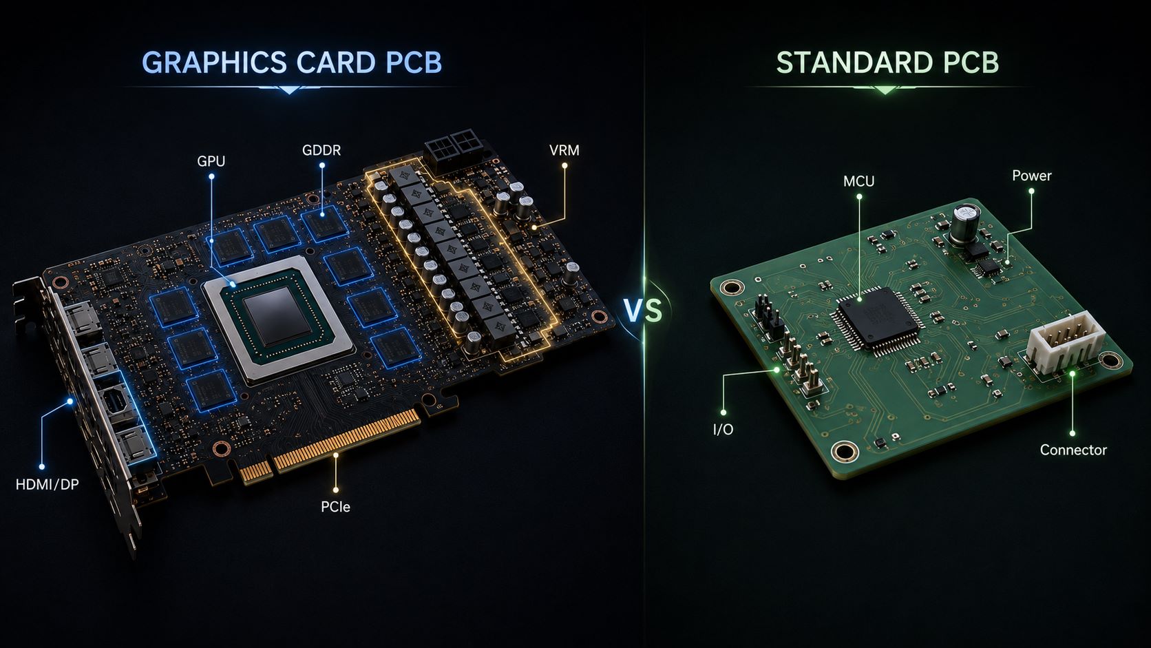
A standard PCB may only handle low-speed control signals and moderate current. A graphics card PCB must handle fast data transmission, high current, dense assembly, and heat at the same time.

The complexity mainly comes from five areas:

  • High-speed signal routing
  • High-current power delivery
  • Fine-pitch BGA assembly
  • Multilayer stack-up control
  • Thermal and mechanical stress

At high speed, PCB traces behave like transmission paths. Trace width, spacing, dielectric thickness, copper thickness, via structure, and reference planes all affect signal quality.

Power delivery is also more demanding. The GPU can draw large and fast-changing current. The PCB must support stable voltage with low resistance copper paths, proper power planes, and well-placed decoupling capacitors.

Thermal stress adds another layer of difficulty. Heat from the GPU, memory, and VRM section must move efficiently through copper areas, vias, solder pads, and cooling contact points.

Mechanical stress should not be ignored either. Long graphics card PCBs may carry heavy heat sinks or fan modules. Poor copper balance or weak structure can increase bending and warpage risk.

This is why graphics card PCB projects should be reviewed from both design and manufacturing perspectives before production starts.

Graphics Card PCB

What Materials Are Used in Graphics Card PCBs?

Most graphics card PCBs use multilayer FR4-based materials. For better thermal stability, high Tg FR4 is often preferred.

Material selection usually depends on:

  • Signal speed
  • Layer count
  • Impedance requirement
  • Copper thickness
  • Thermal load
  • Assembly temperature
  • Cost target
  • Reliability requirement

For higher-speed designs, low-loss materials may be considered. These materials can help reduce signal loss, especially when the board carries fast PCIe, memory, or video output signals.

Copper thickness is another important factor. Power areas may need larger copper planes or thicker copper to carry current and reduce resistance. However, thicker copper also affects etching, line spacing, impedance control, and lamination stability.

Common surface finishes include ENIG and other solderable finishes. ENIG is often selected for fine-pitch assembly because it provides good flatness and stable solderability.

Solder mask color can be green, black, blue, red, white, or other custom colors. For high-density graphics card PCBs, the key concern is not color itself, but solder mask registration, insulation quality, and clearance control.

A practical material choice should balance performance and cost. The best material is not always the most expensive one. It is the material that fits the actual speed, heat, reliability, and production requirements.

Why Does a Graphics Card PCB Need High-Speed Signal Design?

A graphics card PCB transfers data between the GPU, memory, motherboard, and display outputs. These signals must remain stable at high speed.

Main high-speed areas include:

  • PCIe lanes
  • GDDR memory bus
  • HDMI output
  • DisplayPort output
  • Clock signals
  • Control signals

PCIe signals usually use differential pairs. These traces require controlled impedance, length matching, proper spacing, and continuous reference planes.

GDDR memory routing is even more sensitive. The GPU and memory chips must exchange data with precise timing. Poor routing may cause memory instability, signal errors, or reduced performance margin.

HDMI and DisplayPort signals also need controlled routing. Weak layout may cause unstable display output, EMI issues, signal loss, or intermittent failure.

Important high-speed design controls include:

  • Trace width and spacing
  • Differential impedance
  • Length matching
  • Via count and via placement
  • Layer transitions
  • Reference plane continuity
  • Return path quality
  • Crosstalk control

PCB stack-up is closely connected to signal integrity. A well-designed stack-up gives high-speed traces stable reference planes and helps control impedance.

For manufacturing, the PCB factory must control dielectric thickness, copper thickness, trace width, etching tolerance, and lamination quality. Otherwise, the actual impedance may differ from the design target.

How Does a Graphics Card PCB Handle Power and Heat?

Power and heat are two major design concerns in graphics card PCBs.

The main power and heat areas include:

  • GPU
  • GDDR memory
  • VRM power stage
  • MOSFETs
  • Inductors
  • Power input area

The VRM circuit converts input power into stable voltage rails for the GPU, memory, and control circuits. Since GPU current can change quickly, the power path must have low resistance and good transient response.

To support high current, the PCB may use:

  • Wide power traces
  • Large copper planes
  • Multiple vias
  • Thicker copper in power areas
  • Short current paths
  • Proper decoupling capacitor placement

Thermal design also depends on the PCB structure. Heat can move through:

  • Copper planes
  • Thermal vias
  • Component pads
  • Inner copper layers
  • Thermal pads
  • Heat sink contact areas

A strong heat sink or fan is useful, but it cannot solve every thermal problem. If the PCB copper layout, via structure, or component placement is weak, the cooling system may not perform well.

For industrial vision, AI computing, and video processing equipment, thermal reliability is especially important. These systems may operate for long hours under continuous load, so thermal design should be reviewed early.

What Are the Key Manufacturing Challenges of Graphics Card PCBs?

Graphics card PCB manufacturing requires tight control from bare board fabrication to final assembly.

Common fabrication challenges include:

  • Fine line width and spacing
  • High layer count
  • Controlled impedance
  • Dense BGA fan-out
  • Microvias
  • Blind vias
  • Buried vias
  • Via-in-pad design
  • Copper balance
  • Warpage control

Assembly challenges are also important. GPU and memory packages often use BGA structures, which require stable SMT process control.

Key SMT controls include:

  • Solder paste printing
  • SPI inspection
  • Placement accuracy
  • Reflow profile
  • BGA alignment
  • Void control
  • X-ray inspection

Because many solder joints are hidden under BGA packages, visual inspection is not enough. X-ray inspection helps check solder bridges, voids, opens, and alignment issues.

For turnkey PCBA projects, BOM review should be done before assembly. The review should check:

  • Package accuracy
  • Polarity
  • MPN correctness
  • Moisture sensitivity level
  • Lifecycle status
  • Substitute part risk
  • Component availability

Many production delays come from unclear documents or unverified BOM information. Early DFM and BOM review can reduce avoidable mistakes before production.

Graphics Card PCB Manufacturing Case: From Prototype Review to Reliable Assembly

A customer developing an industrial image processing module needed a GPU-based PCB and PCBA solution. The product required stable video processing and long operating time.

The board included:

  • GPU
  • GDDR memory chips
  • PCIe interface
  • HDMI output
  • VRM power stage
  • Sensors
  • Fan control circuit

Before fabrication, the engineering team reviewed the key design files and production risks.

The review focused on:

  • Stack-up design
  • Impedance requirements
  • BGA pad design
  • Power copper areas
  • Thermal via placement
  • Component spacing
  • Assembly process risk
  • Test requirements

The BOM was also checked for:

  • Package size
  • Polarity
  • Part lifecycle
  • Supply risk
  • Possible alternatives

During assembly, the process included:

  • Solder paste printing
  • SPI
  • SMT placement
  • Reflow soldering
  • AOI
  • BGA X-ray inspection
  • Functional test support

The prototype helped the customer verify signal stability, power performance, and thermal behavior before moving to the next production stage.

This type of early review is valuable because many graphics card PCB problems are difficult and costly to correct after mass production begins. Finding risks before fabrication helps improve yield, shorten debugging time, and support a smoother product launch.

Why Work with EBest Circuit for Graphics Card PCB and PCBA Projects?

Graphics card PCB projects need more than basic board fabrication. They require high-speed PCB knowledge, multilayer manufacturing capability, impedance control, BGA assembly experience, and practical engineering support.

EBest Circuit supports customers from prototype review to PCB fabrication, SMT assembly, inspection, and small to medium-volume production.

Our support can include:

  • High-speed PCB manufacturing
  • Multilayer PCB fabrication
  • HDI printed circuit board support
  • Controlled impedance review
  • Stack-up review
  • Material selection support
  • Fine-line PCB production
  • BGA assembly
  • SMT assembly
  • AOI inspection
  • X-ray inspection
  • BOM review
  • DFM review
  • Functional test support

For power and thermal designs, we can help review:

  • Copper distribution
  • Via design
  • High-current paths
  • Thermal via structure
  • Component spacing
  • Assembly risks

For buyers, this support helps reduce common production risks, such as impedance mismatch, BGA soldering defects, power instability, thermal weakness, and unclear assembly requirements.

If your project involves graphics card PCB, GPU-based PCBA, industrial image processing boards, video equipment, or high-speed electronic assembly, EBest Circuit can help review your files and support reliable production from prototype to delivery.

FAQs About Graphics Card PCB

What is a graphics card PCB?
A graphics card PCB is the printed circuit board inside a graphics card. It carries the GPU, memory, power circuit, PCIe interface, video output ports, sensors, and control components.

What components are on a graphics card PCB?
Common components include GPU, GDDR memory, VRM circuit, MOSFETs, inductors, capacitors, BIOS flash memory, PCIe gold fingers, HDMI or DisplayPort connectors, fan headers, and sensors.

Why are graphics card PCBs usually multilayer boards?
They need enough routing space for high-speed signals, power planes, ground planes, memory buses, and control circuits. Multilayer stack-ups also help improve signal integrity and power stability.

What is the difference between a long and short graphics card PCB?
A long PCB provides more space for power circuits, memory layout, connectors, and cooling structure. A short PCB is used when the product needs a compact form factor.

Can a graphics card PCB be cleaned?
It can be cleaned in some cases, but improper cleaning may damage components, connectors, solder joints, or labels. For production, professional cleaning and contamination control are more important than DIY cleaning.

Can a damaged graphics card PCB be repaired?
Minor damage may be repairable. However, BGA failure, internal trace damage, severe bending, or burned power areas are difficult to fix. For production projects, good design and process control are more reliable than repair.

Can a graphics card PCB be replaced?
Replacement is possible only when the board matches the same design, firmware, connector layout, component configuration, thermal structure, and mechanical size.

What files are needed for custom graphics card PCB manufacturing?
Gerber files, drill files, stack-up requirements, impedance requirements, BOM, pick-and-place file, assembly drawing, and test requirements are usually needed.

How do I choose a graphics card PCB manufacturer?
Choose a manufacturer with experience in high-speed PCB, multilayer stack-up, impedance control, BGA assembly, X-ray inspection, DFM review, BOM review, and PCBA testing.

A graphics card PCB, sometimes searched as PCB video card, affects GPU performance, signal stability, power delivery, heat control, and long-term reliability. For high-speed or GPU-based PCBA projects, early review of stack-up, materials, impedance, BOM, and assembly requirements can help reduce production risks. If you need graphics card PCB fabrication, SMT assembly, BGA assembly, X-ray inspection, or engineering support, you can send your Gerber files, BOM, or questions to sales@bestpcbs.com for a practical project review.

You may also like