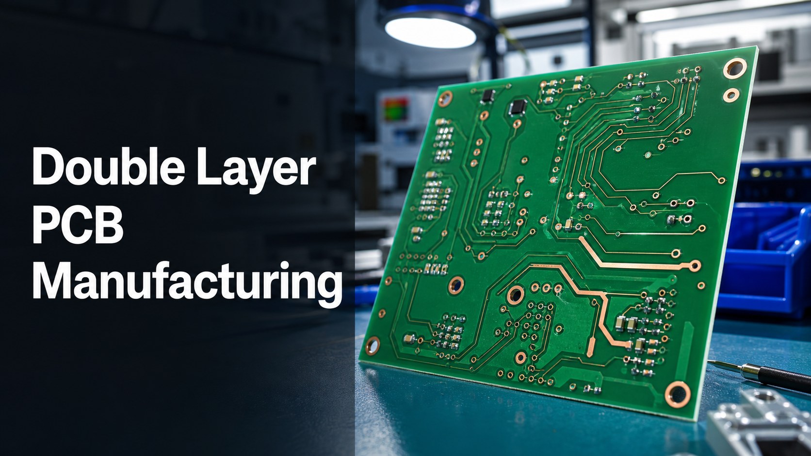
PCB manufacturing PCB manufacturing
Home > Blog

Double Layer PCB

Reliable Double Layer PCB Manufacturing for Prototype and Mass Production
Thursday, June 25th, 2026

Double layer PCB manufacturing is a common choice for electronic products that need more routing space than a single-sided PCB, but do not require the cost or complexity of a multi-layer PCB. This guide explains double layer PCB manufacturing from an engineering and purchasing point of view. It covers the structure, stackup, materials, manufacturing process, layout rules, applications, real production cases, and supplier selection.

Best Technology supports reliable double layer PCB manufacturing from prototype to mass production, with practical process capability for standard FR4, High Tg FR4, FPC, aluminum PCB, and PCB assembly projects. For 2 layer PCB production, we can support common board thicknesses, 1 oz and higher copper options, ENIG, HASL, OSP, immersion silver, immersion tin, and other surface finishes. Our process capability also covers fine line/space, PTH via plating, controlled hole tolerance, solder mask alignment, and SMT panel requirements. If you are developing a new double layer PCB project, pls feel free to send your Gerber files, BOM, stackup, or sample photos to sales@bestpcbs.com. Our engineering team can review your files and provide a practical quotation.

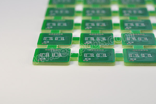
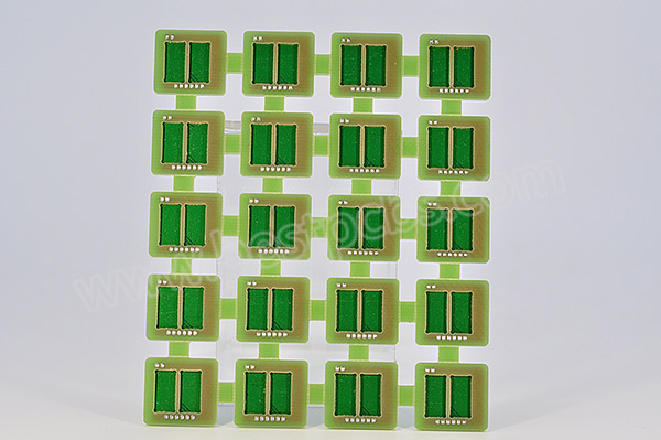
Double layer PCB manufacturing

What Is Double Layer PCB Manufacturing?

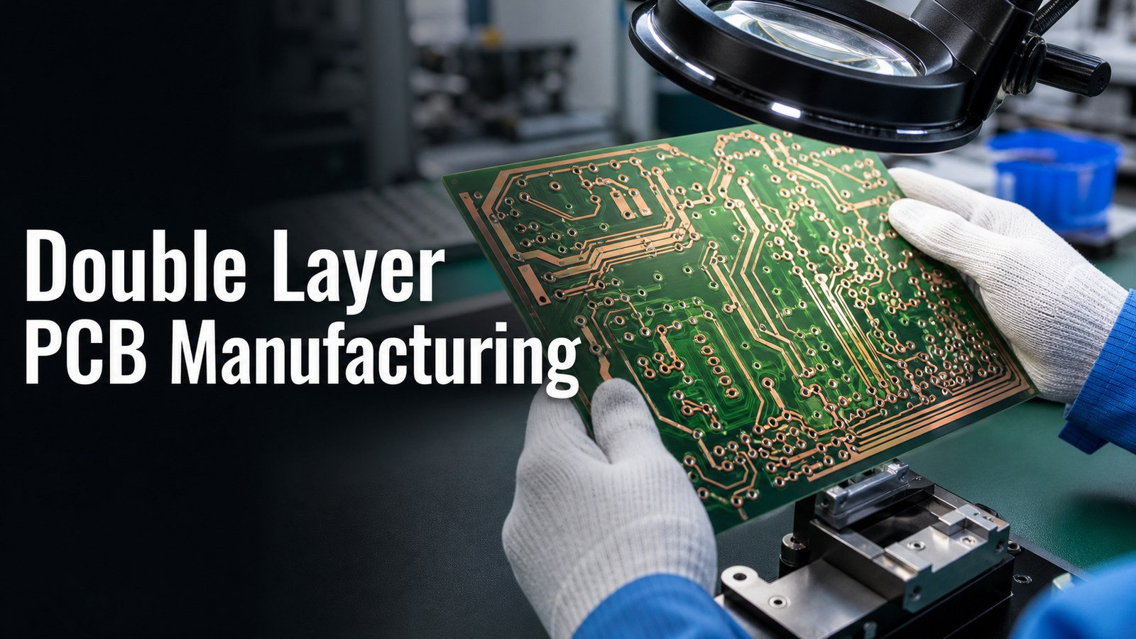
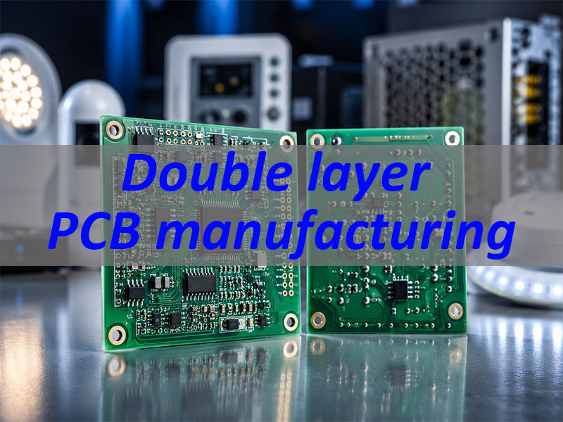
Double layer PCB manufacturing is the process of producing a printed circuit board with copper circuits on both the top and bottom sides. These two copper layers are connected by plated through holes, also called PTH vias, so signals and current can pass between the two sides.

A double layer PCB is also called a double sided PCB, D/S PCB, 2L PCB, 2 layer PCB, or double layer printed circuit board. Unlike a single-sided PCB, it has two conductive layers and supports routing on both sides. Components can also be assembled on one side or both sides, depending on the design and assembly requirements.

The main advantage is better routing flexibility. A 2 layer PCB gives engineers more space for traces, vias, power lines, and component placement, while keeping the cost lower than a 4 layer PCB. For this reason, double layer PCB manufacturing is widely used for prototypes, small batches, and mass production of control boards, sensor modules, power interface boards, and general electronic products.

How Is a Double Layer Printed Circuit Board Structured?

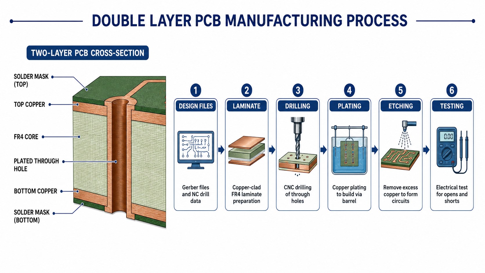
A double layer printed circuit board has a simple structure, but each layer has a clear function. A standard FR4 double layer PCB usually includes solder mask, copper traces, core material, surface finish, and silkscreen on both sides.

StructureFunction
SilkscreenMarks
Surface finishSolderability
Solder maskProtection
Top copperCircuit
FR4 coreInsulation
Bottom copperCircuit
PTH viaLayer connection

The most important part is the PTH via. The hole wall is plated with copper, so the top and bottom copper layers can connect electrically. Without PTH vias, the two sides cannot work as one circuit.

A conventional 2 layer PCB does not use blind vias or buried vias. These structures are normally used in more complex multilayer PCBs. For most double layer PCB manufacturing projects, standard through vias are enough.

What buyers should confirm

Before production, buyers should make sure the hole type is clear. PTH holes are used for electrical connection. NPTH holes are usually used for mounting, positioning, or mechanical support. If this information is unclear, the board may be produced incorrectly.

Buyers should also check via size, annular ring, solder mask opening, board outline, and whether the board needs SMT, DIP, or mixed assembly.

What Is the Standard 2 Layer PCB Stackup?

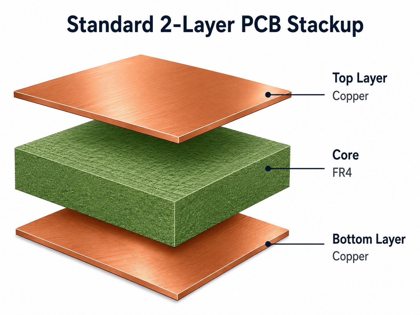
A standard 2 layer PCB stackup is usually simple. It has top copper, core material, and bottom copper. Solder mask, silkscreen, and surface finish are added during production.

Double layer PCB manufacturing

A common 2 layer PCB stackup uses FR4 material, 1.6 mm finished thickness, 1 oz copper, green solder mask, white silkscreen, and HASL or ENIG surface finish. This is a widely used configuration for many standard electronic products.

However, the stackup can be adjusted. The finished thickness may be 0.8 mm, 1.0 mm, 1.2 mm, 1.6 mm, or 2.0 mm. Copper thickness can also change based on current load and thermal needs.

OptionCommon Use
0.8–1.2 mmThin boards
1.6 mmStandard
2.0 mmStronger support
0.5 ozFine circuits
1 ozGeneral use
2 oz+Higher current

Stackup selection should not be based only on price. It should match current load, board size, component weight, assembly method, operating temperature, and mechanical strength.

For simple control circuits, a standard 1.6 mm FR4 stackup is often enough. For industrial or power products, thicker copper, High Tg FR4, or a stronger board thickness may be a better choice.

What Materials Are Used in a 2 Layer Printed Circuit Board?

FR4 is the most common material used in 2 layer printed circuit boards. It offers stable insulation, good mechanical strength, and reasonable cost. This is why it is widely used in control boards, consumer electronics, industrial devices, and general electronic products.

Different applications may need different materials. A product with higher temperature stress may need High Tg FR4. A flexible connection may need PI material. A lighting product with thermal requirements may need aluminum substrate.

MaterialBest For
FR4General PCB
High Tg FR4Heat resistance
CEM-1/CEM-3Cost-sensitive
FR5Higher heat
PIFPC
AluminumHeat dissipation

Surface finish is also part of the material decision. It protects exposed copper and affects solderability. Common options include HASL, lead-free HASL, ENIG, OSP, immersion silver, and immersion tin.

FinishAdvantage
HASLLow cost
Lead-free HASLRoHS
ENIGFlat surface
OSPSMT friendly
Immersion silverGood soldering
Immersion tinFlat pads

ENIG is often used when the design has fine-pitch SMT pads, small components, or higher solderability requirements. HASL is suitable for many standard products and is often more economical.

Buyer note

Material choice should consider working temperature, soldering process, shelf life, current load, assembly complexity, and product reliability. Choosing the right material early can reduce production risk later.

How Does the Double Layer PCB Manufacturing Process Work?

The double layer PCB manufacturing process includes file review, material preparation, drilling, plating, imaging, etching, solder mask, surface finish, profiling, and testing. Each step must be controlled because one weak process can affect the whole board.

Step 1: Engineering file review

  • The manufacturer checks Gerber files, drill files, board outline, copper thickness, surface finish, solder mask color, and special notes. A good DFM review can catch missing drill files, small annular rings, unclear slots, copper too close to the board edge, and panel design problems before production starts.

Step 2: Material preparation

  • The factory prepares the copper clad laminate according to the required material, thickness, and copper weight. The panel size is planned based on board dimensions, quantity, and production efficiency.

Step 3: Drilling

  • Holes are drilled according to the drill file. These holes may include vias, component holes, mounting holes, positioning holes, and slots. Drilling accuracy is important because hole shift can reduce the annular ring and affect reliability.

Step 4: PTH plating

  • After drilling, the hole wall is not conductive. The factory deposits and plates copper inside the hole wall to form a plated through hole. This step connects the top and bottom copper layers.

Step 5: Circuit imaging and etching

  • The circuit pattern is transferred to the copper surface through dry film imaging. After plating and etching, unwanted copper is removed, and the final circuit pattern remains. Etching must be controlled well. Over-etching makes traces too narrow, while under-etching may cause shorts.

Step 6: Solder mask and surface finish

  • Solder mask protects the copper surface and reduces solder bridging during assembly. Surface finish protects exposed pads and improves solderability. The finish should match the assembly process and storage requirements.

Step 7: Profiling and testing

  • The board is routed, V-cut, or milled to shape. Then it goes through electrical test and final inspection. Common checks include open/short test, hole quality, solder mask alignment, surface finish, dimensions, and appearance.

Manufacturing tip

  • Prototype projects usually focus on speed and design validation. Mass production focuses more on repeatability, yield, panel stability, and delivery consistency. A good manufacturer should support both stages.

What PCB Layout Rules Should Be Checked Before Double Layer PCB Manufacturing?

Good PCB layout makes manufacturing easier and more reliable. Before sending files to production, engineers should check trace width, spacing, via design, hole type, copper balance, solder mask, silkscreen, and panelization.

Trace width and spacing

  • Signal traces can be narrow, but power traces need enough width to carry current. Spacing must match voltage and manufacturing capability. Copper-to-edge clearance should also be checked to avoid exposed copper after routing.

Via size and annular ring

  • Vias need enough drill size and pad size. A small annular ring leaves little tolerance for drilling shift. This can affect hole reliability, especially during batch production.

PTH and NPTH definition

  • PTH means plated through hole. NPTH means non-plated through hole. Mounting holes are often NPTH, while electrical holes are usually PTH. This definition should be clear in the drill file or fabrication notes.

Copper balance

  • Copper should be balanced on both sides of the PCB. Large copper imbalance may cause warpage, especially on thin boards, large panels, heavy copper boards, and SMT panels.

Solder mask and silkscreen

  • Solder mask openings should match pad design. Fine-pitch components need enough solder mask bridge. Silkscreen should not cover solder pads because ink on pads may affect soldering.

Panelization for SMT

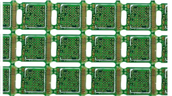
  • If the board needs SMT assembly, panel design becomes important. The panel may need tooling holes, fiducial marks, process edges, V-cut, routing tabs, and a correct feeding direction.

Buyer tip

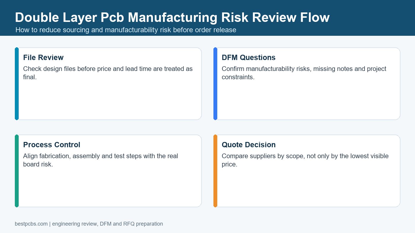
Do not only ask for a PCB price. Ask the supplier to review manufacturability. A simple DFM check before production can prevent many costly changes.

When Should You Choose a 2 Layer Circuit Board?

A 2 layer circuit board is a good choice when the circuit has moderate complexity and can be routed on two sides. It is also suitable when cost, lead time, and production simplicity are important.

Choose 2 Layer WhenReason
Medium densityEasy routing
Moderate speedBasic SI enough
Cost-sensitiveLower cost
Prototype stageFast validation
No blind viasSimple process
Basic groundingCopper pour works

A 2 layer PCB is commonly used in control boards, sensor boards, LED control boards, power interface boards, consumer electronics, industrial terminal boards, and prototype boards. It gives enough routing flexibility for many designs while keeping cost under control.

However, 2 layers may not be enough for high-speed interfaces, dense BGA components, strict EMI control, controlled impedance, complex power networks, or very small board sizes. In those cases, a 4 layer PCB may provide better routing, grounding, and signal performance.

Simple decision rule

Use a 2 layer PCB when the circuit is simple to medium in complexity. Move to 4 layers when routing, EMI, or signal quality becomes difficult.

What Are the Common Applications of Double Layer PCBs?

Double layer PCBs are used across many industries because they balance cost, function, and manufacturability. They are especially suitable for products that need more routing space than a single-sided board but do not need a complex multilayer structure.

Consumer electronics

  • Double layer PCBs are used in chargers, audio devices, remote controls, small appliances, smart home products, and display control boards. These products need stable performance and controlled cost.

Industrial control

  • Industrial boards often use connectors, terminals, relays, sensors, and microcontrollers. A double layer PCB can support these parts well, especially when the design uses both SMT and through-hole components.

LED and lighting products

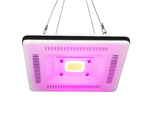
  • Some LED driver boards and lighting control boards use double layer PCBs. If the product has higher thermal requirements, aluminum PCB may be a better option. The choice depends on LED power, heat path, housing design, and assembly method.

Power and battery products

  • Charging boards, battery protection boards, low-power supply boards, and power interface modules can use 2 layer PCBs when current and thermal requirements are manageable. Wider traces and thicker copper may be needed.

Automotive auxiliary electronics

  • Some automotive auxiliary products use double layer PCBs, such as lighting control boards, sensor interfaces, small control modules, and in-car accessories. Material and reliability checks are important for these projects.

2L FPC applications

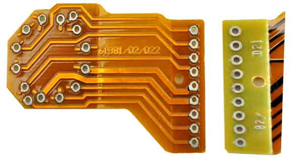
  • A 2L FPC also uses a two-layer circuit structure, but it is flexible rather than rigid. It is used in wearable devices, display modules, camera modules, compact electronics, and flexible interconnections.

Double Layer PCB Case Study: From Prototype to Production

Real production cases show that 2 layer PCB projects are not always simple. Different materials, thicknesses, finishes, and assembly needs create different manufacturing risks.

Case A: 2L FR4 High Tg PCB for stable production

This case is a typical double layer FR4 PCB project with higher material requirements and panel efficiency needs.

ItemSpecification
Type2L FR4
MaterialTg170
Thickness2.0 mm ±10%
Copper1 oz
FinishENIG
Mask/TextGreen/White
ShapeØ8.5 mm
Panel236 × 119.2 mm
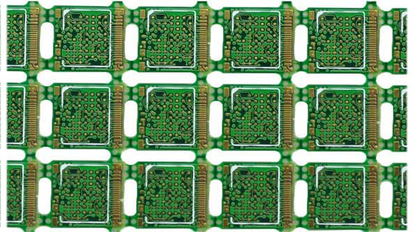
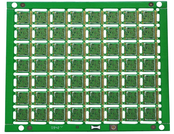
Array105-up

This board uses Tg170 material, which offers better heat resistance than standard FR4. The 2.0 mm thickness improves mechanical strength, while ENIG provides a flat solderable surface for stable assembly. Since the panel contains 105 pieces, the manufacturer must control panel accuracy, routing path, solder mask registration, and electrical testing.

Before mass production, the engineering team should check hole position, board outline, panel spacing, ENIG pad quality, copper balance, fiducial marks, and test method. The goal is not only to make one good sample. The goal is to keep every board stable across the full panel.

Case B: 2L FPC prototype with PI stiffener

This case is useful for flexible electronics where a rigid PCB cannot fit the product structure.

ItemSpecification
Type2L FPC
Copper1/2 oz RA
Base1 mil PI
CoverlayHalf-and-half
Thickness0.116 mm ±0.03
Stiffener0.25 mm PI
Lead time3–4 days

A 2L FPC is much thinner than a rigid FR4 PCB. It needs careful control of bend area, coverlay opening, stiffener position, copper type, and final thickness tolerance. Handling is also important because flexible circuits are easier to deform during production.

Case C: Aluminum PCB with SMT requirements

This case is not a standard FR4 double layer PCB, but it is useful for thermal applications and assembly planning.

ItemSpecification
TypeAluminum PCB
Thickness1.6 mm
Copper1 oz
Thermal1 W
Mask/TextWhite/Black
FinishLead-free HASL
AssemblySMT required

This type of project may require bare board delivery and SMT assembly in the same order. The supplier must check panel design, fiducial marks, process edges, SMT direction, BOM sourcing, remaining material return, and final delivery format.

What buyers can learn

A 2 layer PCB order should not be judged only by layer count. Material, copper weight, board thickness, surface finish, panel design, assembly needs, lead time, and testing requirements all affect manufacturing risk. Clear specifications help the project move from prototype to stable production with fewer revisions.

Double Layer PCB vs 4 Layer PCB Board: Which One Should You Choose?

Double layer PCB and 4 layer PCB are both common. The better choice depends on routing density, signal speed, EMI requirements, cost target, and product reliability.

ItemDouble Layer PCB4 Layer PCB
Layers24
CostLowerHigher
RoutingModerateBetter
EMIBasicBetter
GroundCopper pourPlane possible
Best forSimple/mediumDense/high-speed

Choose a double layer PCB when the circuit is not dense, cost is important, lead time is tight, signal speed is moderate, and basic grounding is enough. It is a strong choice for many control boards, sensor boards, interface boards, and prototypes.

Choose a 4 layer PCB when the board is small but dense, signal lines are many, EMI control is important, high-speed signals are used, or a stable ground plane is required. A 4 layer PCB can improve routing quality and electrical performance.

Do not force a complex design into 2 layers just to reduce PCB cost. A poor 2 layer layout may create noise, failed testing, assembly problems, or redesign cost. The best PCB structure should meet function, cost, reliability, and delivery needs at the same time.

Why Choose Best Technology for Double Layer PCB Manufacturing?

Best Technology supports double layer PCB manufacturing from prototype to mass production. We can help with standard FR4 PCB, High Tg PCB, 2L FPC, aluminum PCB, and PCB assembly projects.

For buyers, this reduces communication gaps between PCB fabrication, assembly, and material sourcing. For engineers, it provides practical manufacturing feedback before production starts.

RequirementSupport
PrototypeFast build
Small batchFlexible quantity
Mass productionStable quality
FR4 / High TgMaterial options
2L FPCFlex support
Aluminum PCBThermal use
AssemblySMT/DIP

Our engineering review can cover Gerber files, drill files, stackup, copper thickness, via design, annular ring, solder mask, surface finish, board outline, panelization, fiducial marks, SMT process edges, BOM, and assembly requirements.

This matters because many PCB problems do not start on the production line. They start from design details, such as unclear hole type, narrow power traces, missing fiducial marks, small via annular rings, poor solder mask bridge, or a surface finish that does not match the assembly process.

Working with one experienced supplier can simplify the project. You can manage PCB fabrication, PCB assembly, BOM sourcing, engineering review, process advice, quality inspection, and delivery planning in one place.

If you need double layer PCB manufacturing, send your Gerber files, BOM, stackup, or sample photos to sales@bestpcbs.com. Our team can review your project and provide a practical quotation.

FAQs about double layer pcb manufacturing

Q1: Is a double layer PCB the same as a 2 layer PCB?
Yes. In most cases, they mean the same thing. Both refer to a PCB with copper circuits on the top and bottom sides.

Q2: What is D/S PCB?
D/S PCB means double sided PCB. It is another name for a double layer PCB or 2L PCB.

Q3: Does a double layer PCB need PTH vias?
Yes. PTH vias are needed when the top and bottom copper layers must connect electrically.

Q4: Does a 2 layer PCB have blind vias or buried vias?
No. A conventional 2 layer PCB uses through vias. Blind vias and buried vias are used in more complex multilayer PCBs.

Q5: What is the standard 2 layer PCB stackup?
A standard stackup includes top copper, FR4 core, and bottom copper. Solder mask, silkscreen, and surface finish are added during production.

Q6: What material is best for double layer PCB manufacturing?
FR4 is the most common choice. High Tg FR4 is better for higher temperature needs. PI is used for 2L FPC. Aluminum substrate is used for thermal applications.

Q7: What copper thickness is common for a 2 layer PCB?
1 oz copper is common for standard boards. Higher copper thickness may be used for power or high-current circuits.

Q8: Can components be assembled on both sides of a double layer PCB?
Yes. Components can be assembled on the top side, bottom side, or both sides.

Q9: Is a double layer PCB cheaper than a 4 layer PCB?
Usually yes. A double layer PCB has fewer layers and a simpler structure. The final price still depends on size, material, copper thickness, finish, and quantity.

Q10: When should I choose a 4 layer PCB instead of a double layer PCB?
Choose a 4 layer PCB when the circuit is dense, high-speed, EMI-sensitive, or difficult to route on two layers.

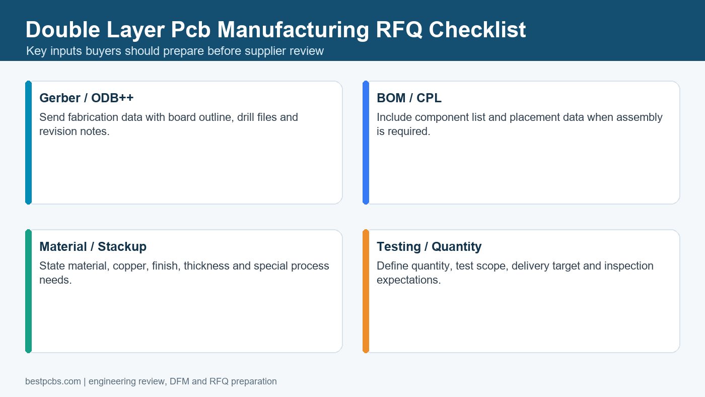
Q11: What files are needed for double layer PCB manufacturing?
You should provide Gerber files, drill files, board outline, stackup, copper thickness, solder mask color, surface finish, and quantity. For assembly, BOM and pick-and-place files are also needed.

Q12: How can I reduce risk before double layer PCB production?
Request a DFM review before production. Check trace width, spacing, via size, annular ring, solder mask, panelization, and assembly requirements.

In conclusion, double layer PCB manufacturing is a reliable choice for many electronic products. It offers more routing space than single-sided PCB and keeps cost lower than many multilayer PCB options.

A good 2 layer PCB project starts with clear specifications. Material, copper thickness, via design, surface finish, panelization, and assembly needs should be confirmed before production.

Best Technology supports double layer PCB manufacturing from prototype to mass production. We can also help with FR4 PCB, High Tg PCB, 2L FPC, aluminum PCB, and PCB assembly.

If you have a new project, send your Gerber files, BOM, or technical requirements to sales@bestpcbs.com. Our engineering team can review your files and provide a practical quotation.

You may also like

Double Layer PCB: Design, Prototyping & Manufacturing Guide
Monday, May 26th, 2025

After spending two decades in the PCB industry and working on countless circuit boards, I’m stoked to dive deep into Double Layer PCBs. These bad boys are the “Swiss Army knives” of the electronics manufacturing world! A Double Layer PCB, or double – sided printed circuit board, has conductive traces laid out on both the front and back of an insulating substrate. These two layers are connected by metallized vias, creating a super efficient electrical pathway.

The perks of Double Layer PCBs are off the charts. They offer high – density routing, allowing for complex circuits to be packed in. They’re cost – effective, making them perfect for large – scale production. And their electrical performance? Rock solid, ensuring lightning – fast and reliable signal transmission. From the smartphones and laptops we use daily to automotive electronics systems and industrial automation gear, Double Layer PCBs are everywhere, powering the core operations of electronic devices.

Double Layer PCB: Design, Prototyping & Manufacturing Guide

What is a Double Layer PCB?

As an experienced PCB process engineer, double layer PCBs hold a special place in my professional journey. Imagine an insulating substrate serving as the core foundation, with copper foils meticulously applied to both the top and bottom surfaces. These copper foils function as parallel “electronic highways,” facilitating the seamless flow of electric current. The insulating material situated between the layers acts as a robust barrier, effectively preventing signal interference and ensuring optimal performance.

The metallized vias play a crucial role, acting as strategic overpasses that connect these two “highways.” This enables current to traverse between the layers with ease, supporting a wide range of intricate circuit functions. It’s precisely this innovative design that forms the bedrock for enhancing the performance capabilities of electronic devices.

Double Layer PCB: Design, Prototyping & Manufacturing Guide

Double Layer PCB Stackup

The structure of a Double Layer PCB is both precise and well – thought – out:

  1. Insulating Substrate: Materials like FR – 4 are commonly used. They’re highly resistant to heat and corrosion, providing stable physical support and electrical insulation for the circuit board, much like a strong foundation for a building.
  2. Top and Bottom Copper Foils: These are the workhorses for current transmission. Their thickness can be flexibly adjusted from 0.5oz to 3oz based on the current – carrying needs of different circuits.
  3. Metallized Vias: They’re the linchpin for connecting the two layers. Without them, the two layers of the circuit simply can’t work together.
  4. Solder Mask Layer: This layer acts as a shield, protecting the copper foils from oxidation and short circuits, almost like a suit of armor for the circuit board.
  5. Silk – Screen Layer: It marks the positions and polarities of components, offering clear instructions for assembly and maintenance down the line.
Double Layer PCB: Design, Prototyping & Manufacturing Guide

Our Services

Design

  • Our 20+ veteran engineers, each with 19+ years of expertise, tackle complex designs effortlessly. We provide end – to – end services including PI, SI analysis, and EMC testing, plus a complimentary DFM check. Our proactive approach identifies production risks early, streamlining the transition from design to high – quality product and saving you time and costs. [Explore more success stories]

Prototyping

Need samples fast? Our 24-hour rush prototyping service delivers quicker than pizza! Plus, our expert engineers offer free technical support—ask us anything, and we’ll explain it clearly. Special requests? We can use premium materials like Rogers or Dupont and implement unique processes. [Learn more about our prototyping process]

Mass Production

Our 8,000㎡ factory, with 18 years of expertise, boasts a 260,000 sq. ft. monthly capacity. Certified by ISO13485 and IATF16949, we ensure top – tier quality for every Double Layer PCB. [Request mass production quote]

Assembly

Our PCB assembly service stands out from the competition. With over 10 SMT production lines in operation and free passive components, it’s a cost – effective solution. Rigorous quality control, including DFM/DFA inspections, functional/ICT tests, X – RAY scans, and dual AOI, ensures top – notch results. We handle SMT, through – hole, BGA, and QFN assembly with ease, and there’s no MOQ. It’s your all – in – one assembly destination. [Learn more about our assembly service perks]

Production Capabilities/Process Capabilities

ItemCapabilities
Layer Count1 – 32 Layers
Max Board Dimension2424″ (610610mm)
Min Board Thickness0.15mm
Max Board Thickness6.0mm – 8.0mm
Copper ThicknessOuter Layer:1oz~30oz, Inner Layer:0.5oz~30oz
Min Line Width/Line SpaceNormal: 4/4mil (0.10mm); HDI: 3/3mil (0.076mm)
Min Hole DiameterNormal: 8mil (0.20mm) ; HDI: 4mil (0.10mm)
Min Punch Hole Dia0.1″ (2.5mm)
Min Hole Spacing12 mil (0.3mm)
Min PAD Ring(Single)3mil (0.075mm)
PTH Wall ThicknessNormal: 0.59mil (15um); HDI: 0.48mil (12um)
Min Solder PAD DiaNormal: 14mil (0.35mm); HDI: 10mil(0.25mm)
Min Soldermask BridgeNormal: 8mil (0.2mm); HDI: 6mil (0.15mm)
Min BAG PAD Margin5mil (0.125mm)
PTH/NPTH Dia TolerancePTH: ± 3mil (0.075mm) ; NPTH: ±2 mil (0.05mm)
Hole Position Deviation±2 mil (0.05mm)
Outline ToleranceCNC: ± 6mil (0.15mm); Die Punch: ± 4mil (0.1mm); Precision Die: ± 2mil (0.05mm)
Impedance ControlledValue>50ohm: ±10%; Value≤50ohm: ±5 ohm
Max Aspect Ratio0.334027778
Surface TreatmentENIG, Flash Gold, Hard Gold Finger, Gold Plating(50mil), Gold finger, Selected Gold plating,ENEPIG, ENIPIG; HAL, HASL(LF), OSP, Silver Imm., Tin Imm
Soldermask ColorGreen/White/Black/Yellow/Blue/Red

Why Choose Us?

Competitive Pricing

We’re all about offering you the best bang for your buck. By streamlining our production processes and building long – term partnerships with top – notch suppliers, we keep costs low without sacrificing an ounce of quality. You’ll get quotes that are hard to beat in the market!

Quality Assurance

Quality isn’t just a buzzword for us—it’s our obsession. From the moment raw materials arrive at our factory to the final product inspection, we have strict quality control measures in place. Only products that pass all our rigorous tests make it to your hands. Each Double Layer PCB you receive is a testament to our commitment to excellence.

Turnkey Solutions

Partnering with us means getting the full package. We handle everything from design and prototyping to mass production and assembly. Say goodbye to juggling multiple suppliers and the headache of excessive communication. We’ll cut down your project timeline significantly. Plus, you’ll have a dedicated sales assistant by your side throughout the process, ready to assist with anything you need.

On – Time Delivery

We know that in the electronics industry, time is money. That’s why we’ve built a robust production planning and logistics system. With our online production status tracking, you can check on your order’s progress anytime. Rest assured, we always deliver on time, ensuring your projects stay on schedule.

Advantages of Double Layer PCBs

  1. Design Flexibility:The double – sided routing opens up a whole new world of circuit layout possibilities. No matter how intricate the circuit design is, we can make it work. It’s also a game – changer for miniaturizing electronic devices, helping pack more functionality into a smaller space.
  2. Cost – Efficiency:Compared to multi – layer PCBs, Double Layer PCBs offer a great balance between performance and cost. For most projects, they deliver the performance you need without breaking the bank, making them a smart choice for budget – conscious customers.
  3. Superior Electrical Performance:Thanks to smart layout and routing designs, along with reliable metallized via connections, signal interference and crosstalk are minimized. This means signals are transmitted quickly and accurately, keeping your devices running smoothly.

Double Layer PCB Production Process/Manufacturing Flow

  1. Design Review:Our engineering team conducts a meticulous review of your design files. We scrutinize every detail, from circuit routing to component selection, to make sure the design aligns perfectly with our manufacturing processes and avoid any potential rework.
  2. Material Procurement:We’re picky when it comes to suppliers. Only the highest – quality insulating substrates, copper foils, and other raw materials make the cut. Each batch undergoes strict testing to ensure they meet our high – performance standards.
  3. Pattern Transfer:Using photolithography techniques, we transfer the circuit pattern onto the copper foil with pinpoint accuracy. Through processes like exposure and development, we ensure the pattern is sharp and in the right place.
  4. Etching:We use etching solutions to remove the unwanted copper, leaving behind the precise conductive traces. Precise control over the etching time and concentration is key to ensuring the traces’ width and spacing match the design specifications.
  5. Drilling and Metallization:Holes are drilled through the substrate to connect the two layers, and then metallized to make the hole walls conductive. The position and size of these holes must be spot – on to guarantee a reliable connection between the layers.
  6. Surface Treatment:Based on your requirements, we choose the right surface treatment process, such as ENIG or HASL. This step enhances the board’s solderability and oxidation resistance, extending its lifespan.
  7. Solder Mask and Silk – screening:We apply solder mask ink to protect the circuit traces from short circuits, leaving only the pads for soldering exposed. Then, we silk – screen component markings, polarities, and other essential information, making assembly and maintenance a breeze.
  8. Assembly and Testing:Electronic components are soldered onto the board, and then we conduct a comprehensive series of functional and quality tests. From basic electrical performance checks to full – scale functionality tests, we leave no stone unturned to ensure the product is up to par.

Problems Solved by Double Layer PCBs

  1. Space Limitations:With the trend of miniaturizing electronic devices, space inside is at a premium. The double – sided routing of Double Layer PCBs solves the dilemma of limited space and complex functionality requirements. It enables devices to pack more features into a compact form factor.
  2. Cost – Performance Trade – off:For projects that need good performance but also have budget constraints, Double Layer PCBs are the perfect fit. They offer a cost – effective way to achieve solid electrical performance, meeting the needs of a wide range of applications.
Double Layer PCB: Design, Prototyping & Manufacturing Guide

Double Layer PCB Design Considerations

When designing Double Layer PCBs, keep these key points in mind:

  1. Circuit Routing:Plan the traces carefully. Isolate high – speed signal lines from potential interference sources and route them separately. Try to separate the power and ground planes as much as possible to reduce power – related signal noise. [Click here for more circuit routing design tips]
  2. Component Placement:Think about heat dissipation and assembly convenience. Place high – power components in well – ventilated areas and make sure they’re easy for workers to handle during soldering and inspection.
  3. Via Design:Be cautious when determining the position and number of vias. Too many can slow down signal transmission, while too few might compromise connection reliability.
  4. Communication:Maintain close communication with your manufacturer. Understanding the manufacturing process limitations helps ensure your design can be produced smoothly without a hitch.

Double Layer PCB Thickness

The thickness of Double Layer PCBs should be chosen based on the specific application:

  • 0.15mm: Ideal for ultra – thin devices with strict thickness requirements, like smartwatches or ultra – thin smartphones.
  • 0.2mm – 0.8mm:Commonly used in small, portable electronics and some consumer products, striking a balance between thinness and circuit layout needs.
  • 1.0mm – 1.6mm:This is the most popular range, widely applied across various electronics. It offers a great compromise between cost and performance and has excellent compatibility.
  • 2.0mm – 3.2mm:Suited for devices with high power requirements and more components, providing extra support and better heat dissipation. It’s often used in industrial control and communication equipment.
  • 6.0 – 8.0mm:Boasting high strength, it can withstand significant mechanical stress. It’s the go – to choice for applications demanding extreme stability, such as automotive engine control modules.

In practice, consider factors like component size, power consumption, and available installation space to pick the perfect thickness and maximize the board’s performance.

Double Layer PCB: Design, Prototyping & Manufacturing Guide

Double Layer PCB Applications

Double Layer PCBs are making waves across multiple industries thanks to their outstanding performance:

  1. Consumer Electronics:They’re the unsung heroes powering devices like smartphones, tablets, and smartwatches, ensuring smooth operation of all functions. [Discover more consumer electronics success stories]
  2. Automotive Industry:Crucial for automotive engine control systems, in – car entertainment, and autonomous driving assistance systems, they keep working reliably even in harsh conditions.
  3. Industrial Field:Providing support for PLCs, industrial robots, and automated production lines, they enable precise control and stable operation.

Whether your project is in the design, prototyping stage, or you’re ready for mass production and assembly, our two – decade – long industry experience, professional team, and comprehensive service system have got you covered. We offer customized solutions tailored to your needs. For more information or to start a collaboration, shoot us an email at sales@bestpcbs.com. Let’s team up and create amazing electronic products together!

You may also like

Double Layer PCB Prototyping & Assembly PCB Manufacturer
Friday, May 23rd, 2025

A Double Layer PCB, also known as a 2-layer PCB, is a type of printed circuit board that consists of two conductive copper layers. These layers are typically located on the top and bottom surfaces of the board, with an insulating substrate material in between. Double Layer PCBs are widely used in various electronic devices due to their ability to accommodate more complex circuits compared to single-layer PCBs, while still being cost-effective and relatively simple to manufacture.

What are the Advantages of Double Layer PCBs?

  • Increased Circuit Complexity: Double Layer PCBs allow for more intricate circuit designs compared to single-layer PCBs, as components can be placed on both sides of the board.
  • Cost-Effective: While offering more functionality than single-layer PCBs, double-layer PCBs remain affordable for many applications.
  • Compact Design: The ability to use both sides of the board enables more compact and space-efficient designs.
  • Improved Signal Integrity: Proper routing on two layers can reduce electromagnetic interference (EMI) and improve signal integrity.
  • Versatility: Double Layer PCBs are suitable for a wide range of applications, from consumer electronics to industrial equipment.

What Problems Can Double Layer PCBs Solve?

Double Layer PCBs address several challenges in electronic design and manufacturing:

  • Space Constraints: They enable more compact designs, making them ideal for devices with limited space.
  • Circuit Complexity: They support more complex circuits without requiring the higher cost of multi-layer PCBs.
  • Signal Interference: Proper routing on two layers can minimize EMI and crosstalk, improving overall performance.

Applications of Double Layer PCBs

Double Layer PCBs are used in a variety of industries and applications, including:

  • Consumer Electronics: Smartphones, tablets, and home appliances.
  • Industrial Equipment: Control systems and automation devices.
  • Automotive Electronics: Sensors, control units, and infotainment systems.
  • Medical Devices: Diagnostic equipment and monitoring systems.
  • Telecommunications: Routers, modems, and communication devices.

Our Services for Double Layer PCBs

At EBest Circuit (Best Technology), we offer comprehensive services for Double Layer PCBs, including:

  • Double Layer PCB Design: Customized design solutions to meet your specific requirements.
  • Double Layer PCB Prototyping: Fast and accurate prototyping to ensure your design works as intended.
  • Double Layer PCB Manufacturing: High-quality production with strict adherence to industry standards.
  • Double Layer PCB Assembly: Full assembly services, including SMT and thru-hole components.

Why Choose Us for Double Layer PCBs?

  • 18+ Years of Experience: With over 18 years in the PCB industry, we have the expertise to deliver high-quality Double Layer PCBs.
  • Competitive Pricing: We offer cost-effective solutions without compromising on quality.
  • Quick Turnaround: Our expedited services ensure your boards are shipped within 24 hours for urgent orders.
  • ISO-Certified Quality: We adhere to IPC standards and can meet Class 2, Class 3, or Class 3A requirements as needed.

Double Layer PCB Manufacturing Capabilities

Parameter Capability
Layers 2
Material FR4, Aluminum, Ceramic, etc.
Board Thickness 0.4mm – 3.2mm
Copper Thickness 0.5oz – 6oz
Minimum Trace/Space 3mil/3mil
Surface Finish HASL, ENIG, OSP, etc.
Solder Mask Green, Blue, Red, etc.
Silkscreen White, Black, etc.

How is a Double Layer PCB Different from Other PCBs?

  • Single-Layer PCBs: Only one conductive layer, limiting circuit complexity.
  • Multi-Layer PCBs: Three or more layers, offering higher complexity but at a higher cost.
  • Double-Layer PCBs: Two conductive layers, striking a balance between complexity and cost.

Contact Us Today

If you have any questions about Double Layer PCBs or would like to request a quote, feel free to contact us. We are committed to providing the best quality, pricing, and services to meet your PCB needs.

You may also like