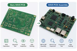
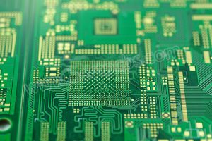
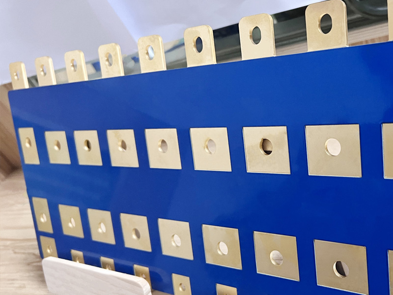
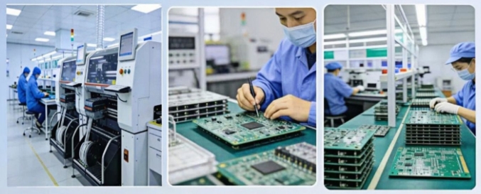
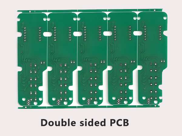
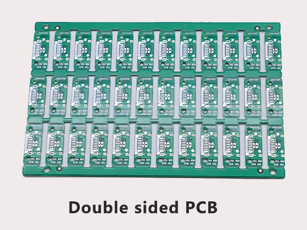
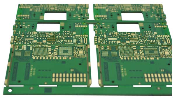
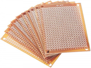
Double layer PCB manufacturing is a common choice for electronic products that need more routing space than a single-sided PCB, but do not require the cost or complexity of a multi-layer PCB. This guide explains double layer PCB manufacturing from an engineering and purchasing point of view. It covers the structure, stackup, materials, manufacturing process, layout rules, applications, real production cases, and supplier selection.
Best Technology supports reliable double layer PCB manufacturing from prototype to mass production, with practical process capability for standard FR4, High Tg FR4, FPC, aluminum PCB, and PCB assembly projects. For 2 layer PCB production, we can support common board thicknesses, 1 oz and higher copper options, ENIG, HASL, OSP, immersion silver, immersion tin, and other surface finishes. Our process capability also covers fine line/space, PTH via plating, controlled hole tolerance, solder mask alignment, and SMT panel requirements. If you are developing a new double layer PCB project, pls feel free to send your Gerber files, BOM, stackup, or sample photos to sales@bestpcbs.com. Our engineering team can review your files and provide a practical quotation.
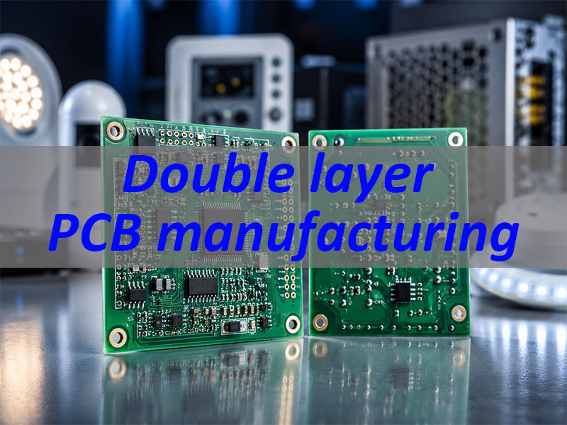
What Is Double Layer PCB Manufacturing?
Double layer PCB manufacturing is the process of producing a printed circuit board with copper circuits on both the top and bottom sides. These two copper layers are connected by plated through holes, also called PTH vias, so signals and current can pass between the two sides.
A double layer PCB is also called a double sided PCB, D/S PCB, 2L PCB, 2 layer PCB, or double layer printed circuit board. Unlike a single-sided PCB, it has two conductive layers and supports routing on both sides. Components can also be assembled on one side or both sides, depending on the design and assembly requirements.
The main advantage is better routing flexibility. A 2 layer PCB gives engineers more space for traces, vias, power lines, and component placement, while keeping the cost lower than a 4 layer PCB. For this reason, double layer PCB manufacturing is widely used for prototypes, small batches, and mass production of control boards, sensor modules, power interface boards, and general electronic products.
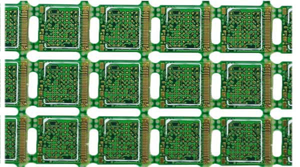
How Is a Double Layer Printed Circuit Board Structured?
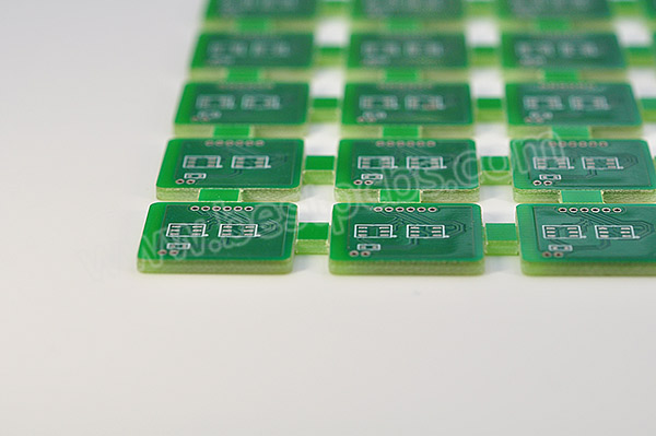
A double layer printed circuit board has a simple structure, but each layer has a clear function. A standard FR4 double layer PCB usually includes solder mask, copper traces, core material, surface finish, and silkscreen on both sides.
| Structure | Function |
|---|---|
| Silkscreen | Marks |
| Surface finish | Solderability |
| Solder mask | Protection |
| Top copper | Circuit |
| FR4 core | Insulation |
| Bottom copper | Circuit |
| PTH via | Layer connection |
The most important part is the PTH via. The hole wall is plated with copper, so the top and bottom copper layers can connect electrically. Without PTH vias, the two sides cannot work as one circuit.
A conventional 2 layer PCB does not use blind vias or buried vias. These structures are normally used in more complex multilayer PCBs. For most double layer PCB manufacturing projects, standard through vias are enough.
What buyers should confirm
Before production, buyers should make sure the hole type is clear. PTH holes are used for electrical connection. NPTH holes are usually used for mounting, positioning, or mechanical support. If this information is unclear, the board may be produced incorrectly.
Buyers should also check via size, annular ring, solder mask opening, board outline, and whether the board needs SMT, DIP, or mixed assembly.
What Is the Standard 2 Layer PCB Stackup?
A standard 2 layer PCB stackup is usually simple. It has top copper, core material, and bottom copper. Solder mask, silkscreen, and surface finish are added during production.
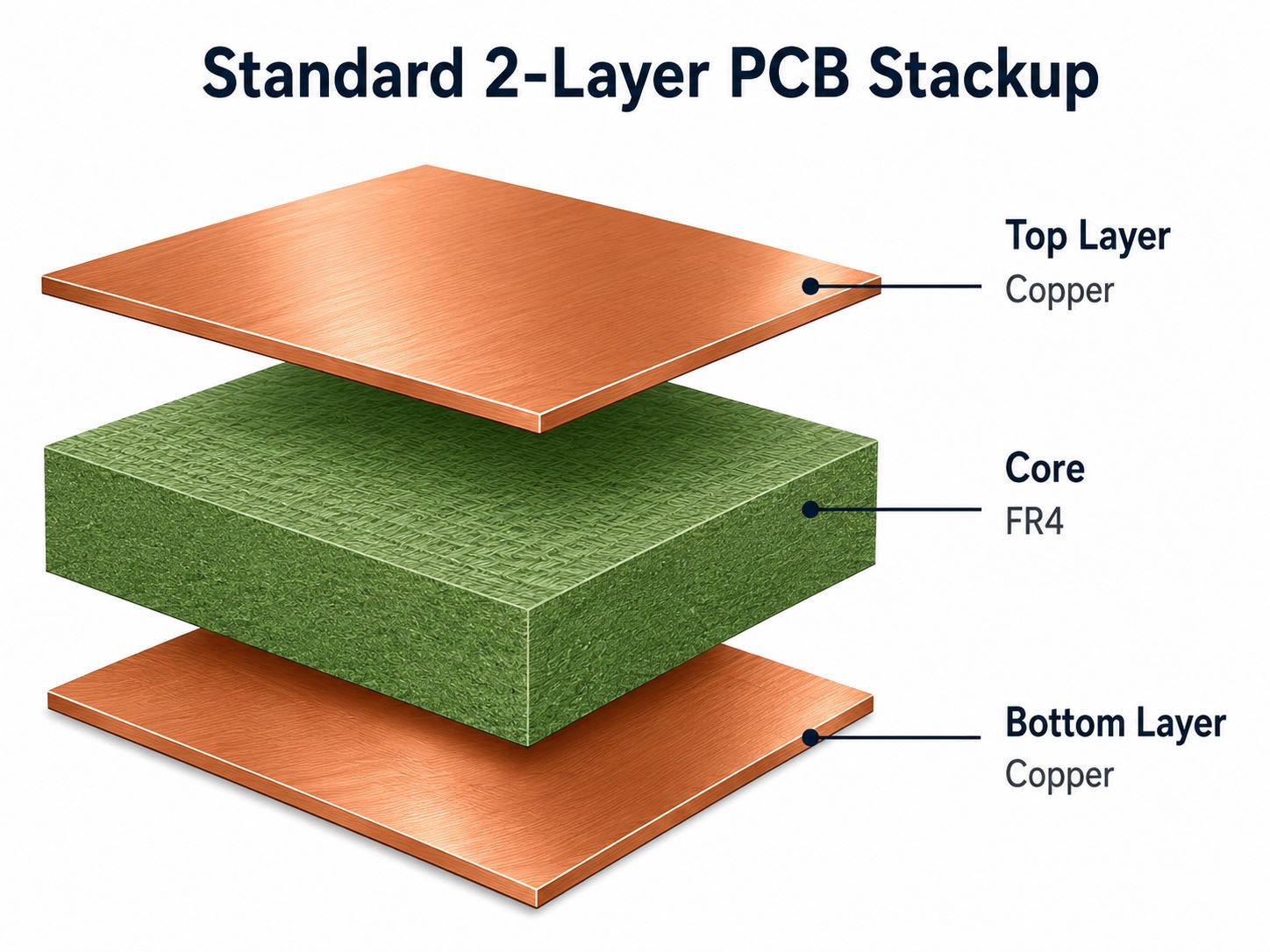
A common 2 layer PCB stackup uses FR4 material, 1.6 mm finished thickness, 1 oz copper, green solder mask, white silkscreen, and HASL or ENIG surface finish. This is a widely used configuration for many standard electronic products.
However, the stackup can be adjusted. The finished thickness may be 0.8 mm, 1.0 mm, 1.2 mm, 1.6 mm, or 2.0 mm. Copper thickness can also change based on current load and thermal needs.
| Option | Common Use |
|---|---|
| 0.8–1.2 mm | Thin boards |
| 1.6 mm | Standard |
| 2.0 mm | Stronger support |
| 0.5 oz | Fine circuits |
| 1 oz | General use |
| 2 oz+ | Higher current |
Stackup selection should not be based only on price. It should match current load, board size, component weight, assembly method, operating temperature, and mechanical strength.
For simple control circuits, a standard 1.6 mm FR4 stackup is often enough. For industrial or power products, thicker copper, High Tg FR4, or a stronger board thickness may be a better choice.
What Materials Are Used in a 2 Layer Printed Circuit Board?
FR4 is the most common material used in 2 layer printed circuit boards. It offers stable insulation, good mechanical strength, and reasonable cost. This is why it is widely used in control boards, consumer electronics, industrial devices, and general electronic products.
Different applications may need different materials. A product with higher temperature stress may need High Tg FR4. A flexible connection may need PI material. A lighting product with thermal requirements may need aluminum substrate.
| Material | Best For |
|---|---|
| FR4 | General PCB |
| High Tg FR4 | Heat resistance |
| CEM-1/CEM-3 | Cost-sensitive |
| FR5 | Higher heat |
| PI | FPC |
| Aluminum | Heat dissipation |
Surface finish is also part of the material decision. It protects exposed copper and affects solderability. Common options include HASL, lead-free HASL, ENIG, OSP, immersion silver, and immersion tin.
| Finish | Advantage |
|---|---|
| HASL | Low cost |
| Lead-free HASL | RoHS |
| ENIG | Flat surface |
| OSP | SMT friendly |
| Immersion silver | Good soldering |
| Immersion tin | Flat pads |
ENIG is often used when the design has fine-pitch SMT pads, small components, or higher solderability requirements. HASL is suitable for many standard products and is often more economical.
Buyer note
Material choice should consider working temperature, soldering process, shelf life, current load, assembly complexity, and product reliability. Choosing the right material early can reduce production risk later.
How Does the Double Layer PCB Manufacturing Process Work?
The double layer PCB manufacturing process includes file review, material preparation, drilling, plating, imaging, etching, solder mask, surface finish, profiling, and testing. Each step must be controlled because one weak process can affect the whole board.
Step 1: Engineering file review
- The manufacturer checks Gerber files, drill files, board outline, copper thickness, surface finish, solder mask color, and special notes. A good DFM review can catch missing drill files, small annular rings, unclear slots, copper too close to the board edge, and panel design problems before production starts.
Step 2: Material preparation
- The factory prepares the copper clad laminate according to the required material, thickness, and copper weight. The panel size is planned based on board dimensions, quantity, and production efficiency.
Step 3: Drilling
- Holes are drilled according to the drill file. These holes may include vias, component holes, mounting holes, positioning holes, and slots. Drilling accuracy is important because hole shift can reduce the annular ring and affect reliability.
Step 4: PTH plating
- After drilling, the hole wall is not conductive. The factory deposits and plates copper inside the hole wall to form a plated through hole. This step connects the top and bottom copper layers.
Step 5: Circuit imaging and etching
- The circuit pattern is transferred to the copper surface through dry film imaging. After plating and etching, unwanted copper is removed, and the final circuit pattern remains. Etching must be controlled well. Over-etching makes traces too narrow, while under-etching may cause shorts.
Step 6: Solder mask and surface finish
- Solder mask protects the copper surface and reduces solder bridging during assembly. Surface finish protects exposed pads and improves solderability. The finish should match the assembly process and storage requirements.
Step 7: Profiling and testing
- The board is routed, V-cut, or milled to shape. Then it goes through electrical test and final inspection. Common checks include open/short test, hole quality, solder mask alignment, surface finish, dimensions, and appearance.
Manufacturing tip
- Prototype projects usually focus on speed and design validation. Mass production focuses more on repeatability, yield, panel stability, and delivery consistency. A good manufacturer should support both stages.
What PCB Layout Rules Should Be Checked Before Double Layer PCB Manufacturing?
Good PCB layout makes manufacturing easier and more reliable. Before sending files to production, engineers should check trace width, spacing, via design, hole type, copper balance, solder mask, silkscreen, and panelization.
Trace width and spacing
- Signal traces can be narrow, but power traces need enough width to carry current. Spacing must match voltage and manufacturing capability. Copper-to-edge clearance should also be checked to avoid exposed copper after routing.
Via size and annular ring
- Vias need enough drill size and pad size. A small annular ring leaves little tolerance for drilling shift. This can affect hole reliability, especially during batch production.
PTH and NPTH definition
- PTH means plated through hole. NPTH means non-plated through hole. Mounting holes are often NPTH, while electrical holes are usually PTH. This definition should be clear in the drill file or fabrication notes.
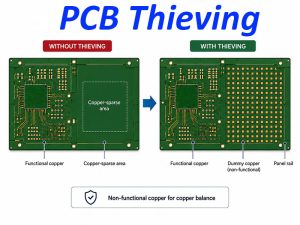
Copper balance
- Copper should be balanced on both sides of the PCB. Large copper imbalance may cause warpage, especially on thin boards, large panels, heavy copper boards, and SMT panels.
Solder mask and silkscreen
- Solder mask openings should match pad design. Fine-pitch components need enough solder mask bridge. Silkscreen should not cover solder pads because ink on pads may affect soldering.
Panelization for SMT
- If the board needs SMT assembly, panel design becomes important. The panel may need tooling holes, fiducial marks, process edges, V-cut, routing tabs, and a correct feeding direction.
Buyer tip
Do not only ask for a PCB price. Ask the supplier to review manufacturability. A simple DFM check before production can prevent many costly changes.
When Should You Choose a 2 Layer Circuit Board?
A 2 layer circuit board is a good choice when the circuit has moderate complexity and can be routed on two sides. It is also suitable when cost, lead time, and production simplicity are important.
| Choose 2 Layer When | Reason |
|---|---|
| Medium density | Easy routing |
| Moderate speed | Basic SI enough |
| Cost-sensitive | Lower cost |
| Prototype stage | Fast validation |
| No blind vias | Simple process |
| Basic grounding | Copper pour works |
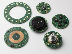
A 2 layer PCB is commonly used in control boards, sensor boards, LED control boards, power interface boards, consumer electronics, industrial terminal boards, and prototype boards. It gives enough routing flexibility for many designs while keeping cost under control.
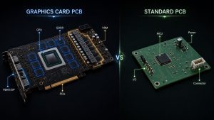
However, 2 layers may not be enough for high-speed interfaces, dense BGA components, strict EMI control, controlled impedance, complex power networks, or very small board sizes. In those cases, a 4 layer PCB may provide better routing, grounding, and signal performance.
Simple decision rule
Use a 2 layer PCB when the circuit is simple to medium in complexity. Move to 4 layers when routing, EMI, or signal quality becomes difficult.
What Are the Common Applications of Double Layer PCBs?
Double layer PCBs are used across many industries because they balance cost, function, and manufacturability. They are especially suitable for products that need more routing space than a single-sided board but do not need a complex multilayer structure.
Consumer electronics
- Double layer PCBs are used in chargers, audio devices, remote controls, small appliances, smart home products, and display control boards. These products need stable performance and controlled cost.
Industrial control
- Industrial boards often use connectors, terminals, relays, sensors, and microcontrollers. A double layer PCB can support these parts well, especially when the design uses both SMT and through-hole components.
LED and lighting products
- Some LED driver boards and lighting control boards use double layer PCBs. If the product has higher thermal requirements, aluminum PCB may be a better option. The choice depends on LED power, heat path, housing design, and assembly method.
Power and battery products
- Charging boards, battery protection boards, low-power supply boards, and power interface modules can use 2 layer PCBs when current and thermal requirements are manageable. Wider traces and thicker copper may be needed.
Automotive auxiliary electronics
- Some automotive auxiliary products use double layer PCBs, such as lighting control boards, sensor interfaces, small control modules, and in-car accessories. Material and reliability checks are important for these projects.
2L FPC applications
- A 2L FPC also uses a two-layer circuit structure, but it is flexible rather than rigid. It is used in wearable devices, display modules, camera modules, compact electronics, and flexible interconnections.
Double Layer PCB Case Study: From Prototype to Production
Real production cases show that 2 layer PCB projects are not always simple. Different materials, thicknesses, finishes, and assembly needs create different manufacturing risks.
Case A: 2L FR4 High Tg PCB for stable production
This case is a typical double layer FR4 PCB project with higher material requirements and panel efficiency needs.
| Item | Specification |
|---|---|
| Type | 2L FR4 |
| Material | Tg170 |
| Thickness | 2.0 mm ±10% |
| Copper | 1 oz |
| Finish | ENIG |
| Mask/Text | Green/White |
| Shape | Ø8.5 mm |
| Panel | 236 × 119.2 mm |
| Array | 105-up |
This board uses Tg170 material, which offers better heat resistance than standard FR4. The 2.0 mm thickness improves mechanical strength, while ENIG provides a flat solderable surface for stable assembly. Since the panel contains 105 pieces, the manufacturer must control panel accuracy, routing path, solder mask registration, and electrical testing.
Before mass production, the engineering team should check hole position, board outline, panel spacing, ENIG pad quality, copper balance, fiducial marks, and test method. The goal is not only to make one good sample. The goal is to keep every board stable across the full panel.
Case B: 2L FPC prototype with PI stiffener
This case is useful for flexible electronics where a rigid PCB cannot fit the product structure.
| Item | Specification |
|---|---|
| Type | 2L FPC |
| Copper | 1/2 oz RA |
| Base | 1 mil PI |
| Coverlay | Half-and-half |
| Thickness | 0.116 mm ±0.03 |
| Stiffener | 0.25 mm PI |
| Lead time | 3–4 days |
A 2L FPC is much thinner than a rigid FR4 PCB. It needs careful control of bend area, coverlay opening, stiffener position, copper type, and final thickness tolerance. Handling is also important because flexible circuits are easier to deform during production.
Case C: Aluminum PCB with SMT requirements
This case is not a standard FR4 double layer PCB, but it is useful for thermal applications and assembly planning.
| Item | Specification |
|---|---|
| Type | Aluminum PCB |
| Thickness | 1.6 mm |
| Copper | 1 oz |
| Thermal | 1 W |
| Mask/Text | White/Black |
| Finish | Lead-free HASL |
| Assembly | SMT required |
This type of project may require bare board delivery and SMT assembly in the same order. The supplier must check panel design, fiducial marks, process edges, SMT direction, BOM sourcing, remaining material return, and final delivery format.
What buyers can learn
A 2 layer PCB order should not be judged only by layer count. Material, copper weight, board thickness, surface finish, panel design, assembly needs, lead time, and testing requirements all affect manufacturing risk. Clear specifications help the project move from prototype to stable production with fewer revisions.
Double Layer PCB vs 4 Layer PCB Board: Which One Should You Choose?
Double layer PCB and 4 layer PCB are both common. The better choice depends on routing density, signal speed, EMI requirements, cost target, and product reliability.
| Item | Double Layer PCB | 4 Layer PCB |
|---|---|---|
| Layers | 2 | 4 |
| Cost | Lower | Higher |
| Routing | Moderate | Better |
| EMI | Basic | Better |
| Ground | Copper pour | Plane possible |
| Best for | Simple/medium | Dense/high-speed |
Choose a double layer PCB when the circuit is not dense, cost is important, lead time is tight, signal speed is moderate, and basic grounding is enough. It is a strong choice for many control boards, sensor boards, interface boards, and prototypes.
Choose a 4 layer PCB when the board is small but dense, signal lines are many, EMI control is important, high-speed signals are used, or a stable ground plane is required. A 4 layer PCB can improve routing quality and electrical performance.
Do not force a complex design into 2 layers just to reduce PCB cost. A poor 2 layer layout may create noise, failed testing, assembly problems, or redesign cost. The best PCB structure should meet function, cost, reliability, and delivery needs at the same time.
Why Choose Best Technology for Double Layer PCB Manufacturing?
Best Technology supports double layer PCB manufacturing from prototype to mass production. We can help with standard FR4 PCB, High Tg PCB, 2L FPC, aluminum PCB, and PCB assembly projects.
For buyers, this reduces communication gaps between PCB fabrication, assembly, and material sourcing. For engineers, it provides practical manufacturing feedback before production starts.
| Requirement | Support |
|---|---|
| Prototype | Fast build |
| Small batch | Flexible quantity |
| Mass production | Stable quality |
| FR4 / High Tg | Material options |
| 2L FPC | Flex support |
| Aluminum PCB | Thermal use |
| Assembly | SMT/DIP |
Our engineering review can cover Gerber files, drill files, stackup, copper thickness, via design, annular ring, solder mask, surface finish, board outline, panelization, fiducial marks, SMT process edges, BOM, and assembly requirements.
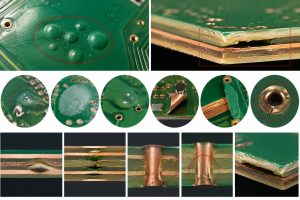
This matters because many PCB problems do not start on the production line. They start from design details, such as unclear hole type, narrow power traces, missing fiducial marks, small via annular rings, poor solder mask bridge, or a surface finish that does not match the assembly process.
Working with one experienced supplier can simplify the project. You can manage PCB fabrication, PCB assembly, BOM sourcing, engineering review, process advice, quality inspection, and delivery planning in one place.
If you need double layer PCB manufacturing, send your Gerber files, BOM, stackup, or sample photos to sales@bestpcbs.com. Our team can review your project and provide a practical quotation.
FAQs about double layer pcb manufacturing
Q1: Is a double layer PCB the same as a 2 layer PCB?
Yes. In most cases, they mean the same thing. Both refer to a PCB with copper circuits on the top and bottom sides.
Q2: What is D/S PCB?
D/S PCB means double sided PCB. It is another name for a double layer PCB or 2L PCB.
Q3: Does a double layer PCB need PTH vias?
Yes. PTH vias are needed when the top and bottom copper layers must connect electrically.
Q4: Does a 2 layer PCB have blind vias or buried vias?
No. A conventional 2 layer PCB uses through vias. Blind vias and buried vias are used in more complex multilayer PCBs.
Q5: What is the standard 2 layer PCB stackup?
A standard stackup includes top copper, FR4 core, and bottom copper. Solder mask, silkscreen, and surface finish are added during production.
Q6: What material is best for double layer PCB manufacturing?
FR4 is the most common choice. High Tg FR4 is better for higher temperature needs. PI is used for 2L FPC. Aluminum substrate is used for thermal applications.
Q7: What copper thickness is common for a 2 layer PCB?
1 oz copper is common for standard boards. Higher copper thickness may be used for power or high-current circuits.
Q8: Can components be assembled on both sides of a double layer PCB?
Yes. Components can be assembled on the top side, bottom side, or both sides.
Q9: Is a double layer PCB cheaper than a 4 layer PCB?
Usually yes. A double layer PCB has fewer layers and a simpler structure. The final price still depends on size, material, copper thickness, finish, and quantity.
Q10: When should I choose a 4 layer PCB instead of a double layer PCB?
Choose a 4 layer PCB when the circuit is dense, high-speed, EMI-sensitive, or difficult to route on two layers.
Q11: What files are needed for double layer PCB manufacturing?
You should provide Gerber files, drill files, board outline, stackup, copper thickness, solder mask color, surface finish, and quantity. For assembly, BOM and pick-and-place files are also needed.
Q12: How can I reduce risk before double layer PCB production?
Request a DFM review before production. Check trace width, spacing, via size, annular ring, solder mask, panelization, and assembly requirements.
In conclusion, double layer PCB manufacturing is a reliable choice for many electronic products. It offers more routing space than single-sided PCB and keeps cost lower than many multilayer PCB options.
A good 2 layer PCB project starts with clear specifications. Material, copper thickness, via design, surface finish, panelization, and assembly needs should be confirmed before production.
Best Technology supports double layer PCB manufacturing from prototype to mass production. We can also help with FR4 PCB, High Tg PCB, 2L FPC, aluminum PCB, and PCB assembly.
If you have a new project, send your Gerber files, BOM, or technical requirements to sales@bestpcbs.com. Our engineering team can review your files and provide a practical quotation.