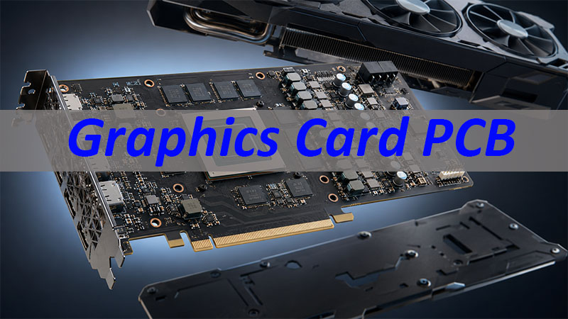
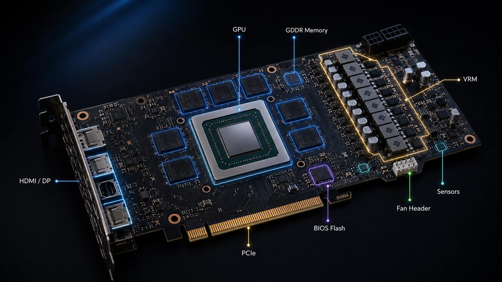
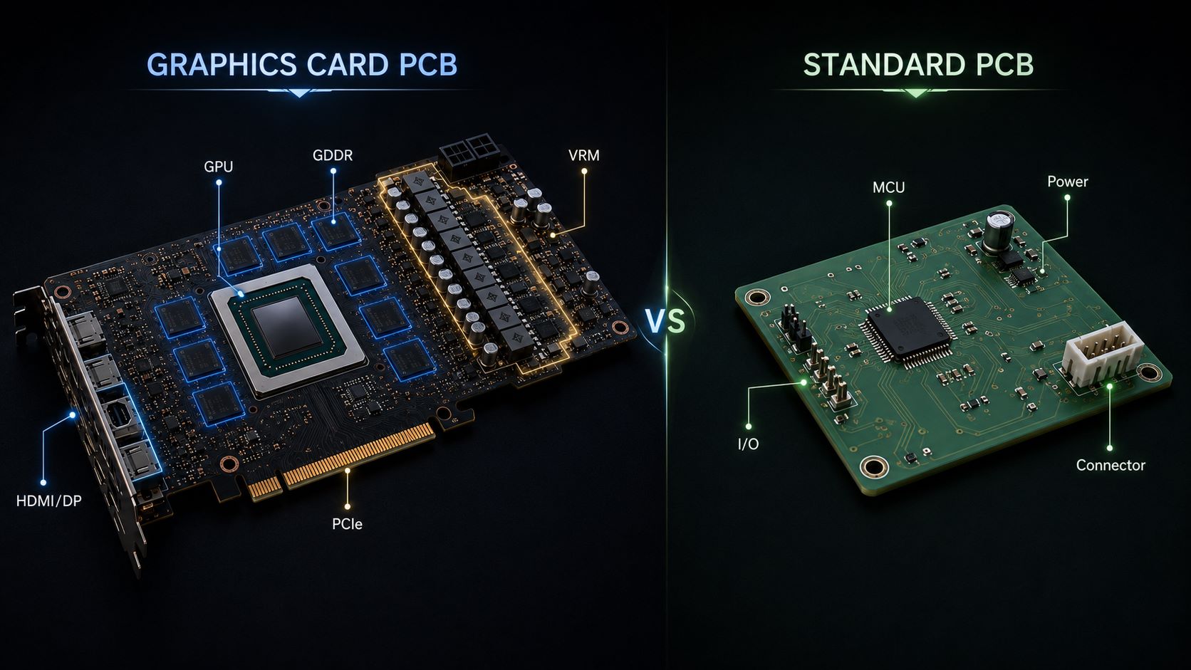
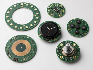
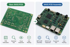
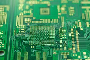
A PCB GPU is the graphics card circuit board that connects the processor, video memory, power stages, PCIe interface, display outputs and control circuits. Its architecture is shaped by the GPU package, memory bus, power target, cooler geometry and manufacturing limits. This guide explains how reference and custom graphics card PCB designs differ, then follows the board from functional zoning and stackup planning through fabrication, BGA assembly and validation.
What Is a PCB GPU in a Graphics Card?
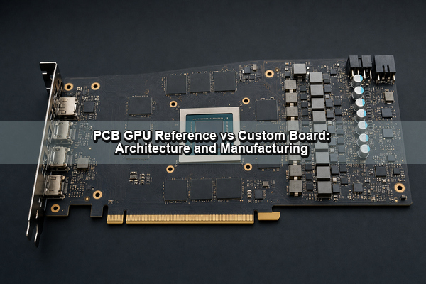
A PCB GPU is not the silicon processor by itself. The GPU is a packaged semiconductor mounted to the board, usually with a dense ball grid array. The graphics card PCB is the larger electrical and mechanical platform that distributes power, routes memory and PCIe signals, stores firmware, supports display interfaces and transfers heat into the cooling assembly.
The board also differs from a complete graphics card. A finished card includes the assembled PCB, heatsink, fans or cold plate, thermal interface materials, bracket, backplate and enclosure parts. This distinction matters because a board can meet its electrical targets yet fail as a product if mounting pressure, airflow, connector alignment or thermal-pad compression is incorrect.
The existing BestPCBs GPU PCB overview explains the basic components and operating path. The focus here is the engineering relationship between the board architecture and the processes needed to build it consistently.
Reference PCB vs Custom PCB GPU: What Changes?
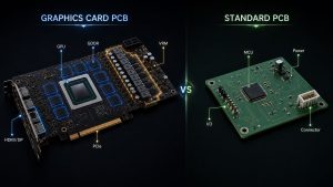
A reference PCB is a baseline design associated with a GPU platform. It establishes a proven relationship among the processor, memory devices, power system, firmware, interfaces and cooling envelope. A custom board keeps the processor platform but may change the outline, VRM phase count, connector placement, memory population, display outputs, sensing, cooling attachment or mechanical support.
| Design Area | Reference Board | Custom Board |
|---|---|---|
| Board outline | Follows the baseline mechanical envelope | May be shorter, taller or shaped for a specific cooler or enclosure |
| Power stages | Uses the baseline rail and phase arrangement | May change phase count, component rating, connectors or telemetry |
| Memory | Uses the validated package and placement plan | May change population while remaining within controller and firmware limits |
| Cooling | Matches the reference mounting and contact geometry | Requires new keep-outs, pressure distribution and thermal-interface checks |
| Validation | Starts from an established implementation | Requires renewed electrical, thermal, mechanical and production validation |
Custom does not mean unconstrained. Package pinout, memory topology, interface requirements and platform documentation still govern the design. A shorter board may reduce available routing and copper area. A stronger VRM may increase heat density and component height. A different cooler may alter board bending and the pressure applied to large BGA packages. Every architectural change creates linked electrical and mechanical checks.
How Is a PCB GPU Divided into Functional Zones?
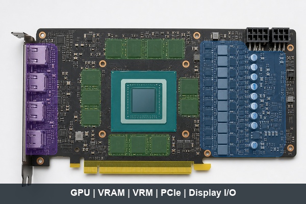
A practical board review begins by separating the layout into functional zones. This makes current paths, high-speed routes, heat sources and mechanical constraints easier to evaluate than a component-by-component inspection.
- GPU BGA zone: contains the processor footprint, local decoupling, escape routing and nearby reference planes.
- Memory zone: places GDDR devices around the processor or connects the package to another high-bandwidth memory architecture.
- VRM zone: includes controllers, power stages, inductors, bulk capacitors, current sensing and low-voltage distribution.
- Host-interface zone: carries PCIe lanes, reference clocks, sideband signals and the edge connector.
- Display and I/O zone: contains output connectors, protection devices, retimers or level-shifting circuits where required.
- Control zone: supports firmware, fan control, temperature and voltage monitoring, and board identification.
- Mechanical and thermal zone: covers mounting holes, keep-outs, backplate contact, thermal pads and cooler load paths.
The zones are electrically connected but should not be laid out as one undifferentiated area. Switching nodes in the VRM require short, compact loops. Memory links require consistent geometry and uninterrupted references. Mounting holes need copper and component clearances. A board-level schematic may show connectivity, while a placement view reveals whether those functions can coexist without creating noise, heat or assembly problems.
How Should the Stackup Be Planned for a PCB GPU?
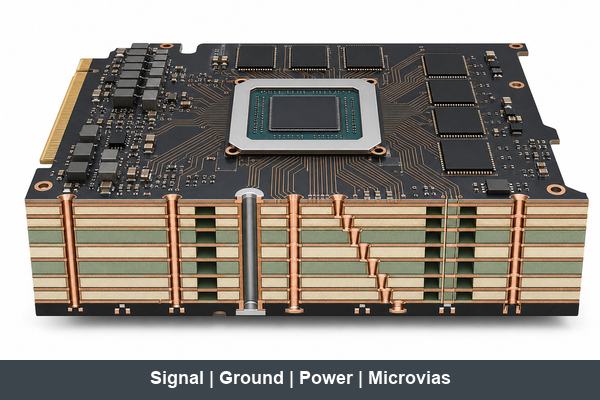
The layer count is an outcome of routing density, reference-plane needs, power distribution and fabrication capability; it is not a universal GPU specification. A compact consumer card, a workstation accelerator and a multi-GPU server baseboard may need very different stackups. Claims that every GPU board requires one fixed layer count should therefore be treated cautiously.
Start with the signal groups and the plane structure they require. PCIe and memory layers need stable reference planes and controlled dielectric thickness. Power rails need enough copper area and low-inductance return paths. Dense BGA escape may require blind vias, buried vias, via-in-pad or sequential lamination. The final stackup must also remain symmetric enough to control bow and twist during lamination and reflow.
- Place high-speed signal layers next to continuous ground references.
- Separate noisy power conversion from sensitive signal routing.
- Assign power and ground planes according to current and return-path requirements.
- Control resin content and copper balance across the construction.
- Limit sequential lamination cycles to a structure the fabricator can register reliably.
- Match finished copper thickness and dielectric values to the impedance model.
When fanout density exceeds conventional through-hole routing, an HDI PCB structure can free routing channels beneath the processor and memory packages. HDI should be used where it solves a real escape or signal problem, because each microvia level adds registration, plating and reliability considerations.
How Are PCIe and Memory Signals Routed?
PCIe and graphics-memory interfaces are routed as transmission structures, not ordinary point-to-point wires. Their behavior depends on trace geometry, dielectric properties, reference continuity, coupling, via transitions and the package models at both ends. The exact target impedance and timing limits come from the applicable platform documentation, not from a generic internet rule.
For PCIe lanes, the designer controls differential geometry, insertion loss, return loss, skew and discontinuities across connectors and vias. Layer changes need nearby return-path transitions. Stubs may require backdrilling or an alternative via structure at higher data rates. Reference-plane splits, poorly placed anti-pads and long uncoupled sections can produce reflections or mode conversion even when the route length appears correct.
Memory routing is usually shorter but more topologically constrained. Package escape, byte-lane grouping, address or command routing, data-lane matching and device placement must be solved together. Length matching is not simply making every line identical; it is meeting the timing budget while controlling crosstalk and avoiding unnecessary serpentine sections. Manufacturing variation in copper thickness, etching and dielectric thickness should be included in the model.
An impedance control PCB process links the design model to the real board through stackup confirmation, impedance coupons and measured results. The same material designation can have different pressed thickness or resin behavior in different constructions, so final impedance should be based on the production stackup.
How Should VRM and Power Planes Be Designed?
The VRM converts input power into the low-voltage, high-current rails required by the processor and memory. Its PCB design must minimize conduction loss, switching-loop inductance, voltage droop and heat concentration. The most important geometry is the complete current loop, including the return path, rather than the width of one visible trace.
Power stages, input capacitors and inductors should be arranged to shorten high di/dt loops. Output capacitors and local decoupling must connect to the load through low-inductance paths. Plane transitions use multiple appropriately sized vias, with attention to current sharing and the thermal effect of drilling away copper. Narrow neck-downs, isolated copper islands and poorly stitched layers can undo the benefit of a large plane.
Copper weight is selected with the whole stackup in mind. Thicker copper can reduce DC resistance and spread heat, but it also changes etching capability, minimum spacing, dielectric fill, lamination behavior and impedance geometry. A mixed construction may use different copper weights by layer, provided copper balance and manufacturability remain controlled.
How Does Thermal Design Affect the PCB?
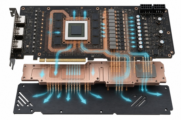
The board is part of the thermal path, but it is not the only heat-removal element. Heat moves through package solder joints, copper planes, thermal vias, interface pads, heatsinks, backplates and airflow. Improving one path does not guarantee a lower junction temperature if another interface dominates the thermal resistance.
GPU, memory and power stages create different heat maps. The processor normally transfers most heat through its top-side cooling interface, while the PCB still spreads heat from the package and local decoupling area. Power stages and memory devices may depend more heavily on copper spreading, via arrays and thermal-pad contact to the cooler or backplate. The via pattern must respect BGA escape, plane continuity and solderability instead of filling every open area indiscriminately.
Thermal-interface thickness must match the mechanical gap and compression range. A pad that is too thin may not contact; one that is too thick or stiff may bend the board or reduce pressure on the processor interface. Temperature cycling can then combine material expansion, board flex and BGA solder strain. Thermal simulation, mechanical tolerance analysis and physical temperature measurement should therefore agree before the cooling structure is released.
Which PCB Materials Fit Different GPU Board Classes?
Material selection begins with the required loss, thermal reliability, z-axis expansion, glass-transition behavior and fabrication process. Standard or high-Tg FR4 PCB materials may be suitable for many graphics-card constructions. Lower-loss laminates become more relevant as channel loss, layer length and interface speed consume the available signal budget.
| Material Direction | Where It Fits | Engineering Tradeoff |
|---|---|---|
| General high-Tg FR-4 | Shorter channels and moderate board complexity | Economical and widely processed, but loss must be checked against the real channel budget |
| Low-loss FR-4 class | Faster PCIe or longer routed channels | Improved signal performance with tighter material and stackup control |
| Very-low-loss laminate | High-end accelerator or long high-speed links | Higher material and processing cost; availability and compatibility need confirmation |
| Hybrid construction | Selected high-speed layers combined with conventional layers | Can target performance where needed, but lamination compatibility and registration are more complex |
Datasheet Dk and Df values are not enough by themselves. The test method, frequency, resin content, glass style and pressed thickness affect the working model. Copper roughness can also contribute meaningful loss. Material approval should therefore be tied to the stackup and channel simulation rather than a trade name alone.
What Mechanical Limits Matter Around the Cooler and PCIe Edge?
A graphics card board carries a heavy cooling assembly while being supported by the PCIe connector, bracket, fasteners and sometimes a backplate or chassis brace. Mounting-hole position, screw torque, spacer height and cooler flatness determine how that load reaches the laminate and BGA packages.
Keep copper, traces, vias and small components away from high-stress mounting regions according to the mechanical model. Large cutouts, edge notches and dense perforation can reduce local stiffness. The PCIe edge requires controlled outline dimensions, bevel geometry, plating thickness and positional accuracy so the card mates correctly without excessive insertion stress.
A custom short board, tall board or dual-board assembly changes the load path and airflow. Connector stacks and board-to-board links also introduce tolerance accumulation and high-speed discontinuities. Mechanical CAD, PCB data and cooler drawings should be reviewed as one assembly before tooling is released.
How Is a PCB GPU Fabricated?
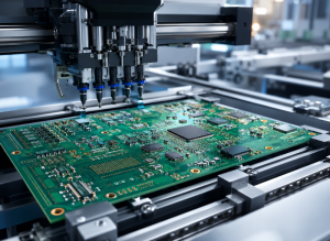
Fabrication follows the normal multilayer PCB sequence, but dense fanout, controlled impedance and thick or mixed copper make several stages more sensitive. The fabricator first confirms the production stackup, drill plan, impedance structures, copper distribution and sequential-lamination sequence. Inner layers are imaged and etched, inspected, treated for bonding and laminated under controlled pressure and temperature.
Mechanical and laser drilling are assigned according to via type. Blind microvias are formed at the correct sub-stack stage, then desmeared, metallized and plated. Via-in-pad structures may require conductive or nonconductive fill, planarization and copper capping before fine-pitch imaging. Registration data from each build stage helps determine whether the design tolerances remain achievable.
After outer-layer imaging and plating, the board receives solder mask, surface finish, legend and profile routing. ENIG or another finish may be used according to pad, connector and assembly requirements; the PCIe fingers may need a separate hard-gold process. Finished boards are electrically tested, and controlled-impedance constructions are measured using coupons correlated to the production panel.
EBest Circuit (Best Technology) supports multilayer boards up to 32 layers and HDI structures up to 3+N+3, with HDI line/space capability down to 2/2 mil and minimum holes down to 0.10 mm. These are maximum advertised capabilities and remain subject to material, stackup, board dimensions, design complexity and engineering review.
Why Is GPU and Memory BGA Assembly Difficult?
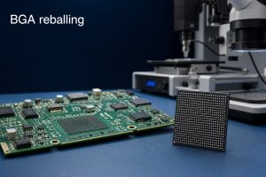
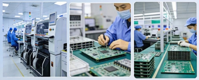
Large GPU packages and closely spaced memory BGAs create hidden solder joints, dense local thermal mass and tight coplanarity requirements. Solder-paste transfer must be uniform across the package area. Placement accuracy, package warpage, board warpage and the reflow thermal profile then determine whether every ball collapses and wets correctly.
Moisture-sensitive components require controlled storage and baking according to their classification and exposure history. The reflow profile must satisfy the solder alloy while limiting excessive thermal gradients across the board. Heavy copper and large heatsinking areas can slow heating, while thin local sections heat faster. One profile copied from a different product may therefore create head-in-pillow, non-wet opens, voiding or component shift.
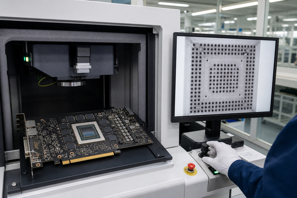
Inspection needs to match the hidden-joint risk. AOI can verify polarity, placement and visible joints but cannot see beneath a BGA. X-ray inspection reveals missing balls, bridges, gross voiding and alignment. Process development may also use cross-section analysis, dye-and-pry or other destructive methods on qualification samples when the reliability target requires it.
For production that includes fine-pitch packages, EBest Circuit offers PCB assembly, BGA assembly and X-ray inspection. The advertised minimum BGA pitch is 0.25 mm, subject to package, board, stencil, component and process review.
Which Tests Validate a PCB GPU?
Validation should connect design assumptions to measurable board and assembly results. No single inspection covers every failure mode, so tests are selected by process stage and risk.
- Inner-layer and final AOI: checks pattern defects, opens, shorts and dimensional anomalies before they become hidden.
- Microsection: verifies plated-hole quality, microvia structure, layer registration and copper thickness on representative coupons.
- Electrical test: confirms net continuity and isolation on the bare board.
- Impedance measurement: compares test coupons with specified controlled-impedance targets.
- SPI and assembly AOI: monitor solder-paste deposits, placement, polarity and visible solder conditions.
- X-ray inspection: evaluates hidden GPU, memory and power-package joints.
- Power-rail bring-up: checks sequencing, short-circuit behavior, rail regulation and current draw before full load.
- Functional and thermal test: exercises memory, interfaces and processing load while monitoring voltage, temperature and stability.
- Reliability qualification: may add temperature cycling, vibration or mechanical tests according to the application environment.
Measurement limits must come from the design and product requirements. A generic pass/fail value for BGA voiding, impedance tolerance or thermal cycling cannot replace package, interface and reliability criteria that apply to the actual board.
FAQs About PCB GPU Boards
How many layers does a GPU PCB have?
There is no fixed layer count. It depends on package escape, memory width, PCIe generation, power-plane needs, board size and the use of HDI. Consumer graphics cards, workstation boards and AI accelerator baseboards can use substantially different constructions.
Is a GPU the same as a graphics card PCB?
No. The GPU is the processing device. The graphics card PCB carries that device and connects it to memory, power conversion, the host interface, display circuits and control functions.
Does every PCB GPU need HDI?
No. HDI becomes appropriate when the package fanout, routing density or form factor cannot be solved efficiently with conventional through vias. Some boards can use mechanically drilled blind or buried structures, while denser designs may require laser microvias and sequential lamination.
Why do custom graphics cards use different PCBs?
Manufacturers may change board dimensions, power stages, connectors, component selection, cooling attachment and output configuration. The processor platform still imposes electrical and firmware constraints, so a custom design is a controlled adaptation rather than a free redesign.
Can one stackup be reused for every graphics card?
No. The stackup must match the interface speeds, routing density, copper distribution, board thickness, material set and fabrication process. Reuse is possible only after confirming that those constraints remain equivalent.
Conclusion
A PCB GPU succeeds when processor fanout, memory timing, PCIe channels, VRM current, thermal interfaces and cooler mechanics are engineered as one board system. Reference designs reduce uncertainty, while custom boards can change size, power and cooling only after the linked electrical and mechanical effects are revalidated.
EBest Circuit (Best Technology) supports high-layer-count, HDI, controlled-impedance PCB fabrication and fine-pitch BGA assembly for complex computing hardware. For technical questions about a graphics card or accelerator board, contact sales@bestpcbs.com.