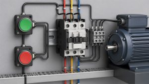
A buck converter PCB must convert voltage efficiently while keeping heat, EMI, ripple and voltage stability under control. The schematic may look simple, but poor layout can cause noise, unstable output, hot components, failed EMC testing or unstable batch production.
Are You Worried About These Problems in Buck Converter PCB Projects?
- Delivery delays: Unclear Gerber files, BOM changes, slow sample approval, component shortages, or repeated layout revisions may delay your prototype and batch production schedule.
- Hidden costs: Extra charges may appear after quotation approval, including copper thickness changes, material upgrades, stencil adjustments, component replacement, thermal redesign, testing fees, or assembly rework.
- Quality instability: Poor hot loop control, weak grounding, insufficient copper area, wrong input capacitor placement, or unstable SMT process may cause EMI failure, high ripple, overheating, soldering defects, or unstable output voltage.
As a 20+ years PCB manufacturer, EBest Circuit provides buck converter PCB manufacturing, prototype, assembly, DFM review, and testing support for global power electronics projects, OEM factories, and industrial control applications. Below are our solutions to above problems:
- Delivery predictability: Fast DFM review, ERP + MES production tracking, prototype schedule control, BOM checking, and production progress follow-up help reduce approval delays and improve delivery stability.
- Cost transparency: BOM-level cost review confirms material, copper thickness, fabrication, assembly, testing, packaging, and export documentation before production, helping customers avoid hidden redesign and rework costs.
- Quality reliability: AOI inspection, flying probe testing, solder paste control, thermal validation, ripple testing, power-on testing, and functional testing help verify converter reliability before shipment.
Welcome to contact us if you have any request for buck converter PCB manufacturing, prototype, design review, or assembly: sales@bestpcbs.com.
What Is a Buck Converter PCB and Where Is It Used?
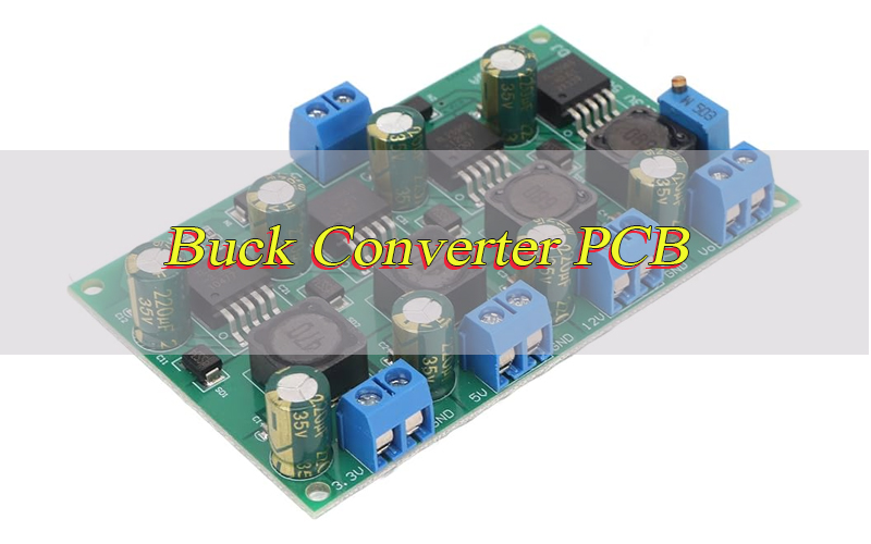
A buck converter PCB is a printed circuit board used for a step-down DC-DC power converter. It reduces a higher DC input voltage to a lower regulated DC output voltage with better efficiency than many linear regulator solutions.
A typical buck converter circuit board includes a switching IC or controller, MOSFET, inductor, input capacitor, output capacitor, diode or synchronous rectifier, feedback network and protection components.
Common applications include:
- Industrial control modules
- LED lighting drivers
- Battery-powered devices
- Automotive auxiliary power
- IoT power boards
- Telecom and communication equipment
- Motor control systems
- Embedded controller boards
- Consumer electronics power rails
What Should Be Confirmed Before Starting a Buck Converter PCB Project?
After the application and circuit function are clear, the next step is to confirm the electrical and manufacturing requirements before layout or quotation. A buck converter PCB project should not start with Gerber files alone because input voltage, output current, ripple target and thermal limits directly affect layout, copper thickness and testing.
Key items to confirm before production:
| Item | Typical Range |
|---|---|
| Input voltage | 5V, 12V, 24V, 48V or custom |
| Output voltage | 1.2V, 3.3V, 5V, 12V or custom |
| Output current | 0.5A–30A+ |
| Switching frequency | 100kHz–3MHz |
| Copper thickness | 1oz–4oz+ |
| Board layers | 2L, 4L, 6L or higher |
| Material Tg | 135°C, 150°C, 170°C+ |
| Surface finish | HASL, ENIG, OSP |
| Testing | AOI, flying probe, ICT, functional test |
Before layout approval, the schematic, BOM, datasheet reference layout and operating environment should be checked together.
How Should Buck Converter PCB Design Balance Efficiency, Heat and Stability?
Buck converter PCB design should balance efficiency, heat and stability at the same time. A converter may reach the correct output voltage during a simple test, but it can still fail later if copper resistance is too high, the thermal path is weak, or the feedback loop is affected by switching noise.
- Reduce copper resistance in high-current paths: Input current, output current and ground return paths should use short and wide copper. Narrow traces increase voltage drop and heat rise, especially when the output current reaches several amps or more.
- Select copper thickness based on current and temperature rise: Standard 1oz copper may work for low-current power rails. For higher current or compact boards, 2oz, 3oz or heavier copper may be needed to reduce temperature rise and improve current capacity.
- Keep power components thermally connected: Switching ICs, MOSFETs, diodes and inductors should have enough copper area around their pads. Exposed pads should connect to thermal vias when the datasheet recommends bottom-layer heat spreading.
- Prevent inductor saturation: The inductor should be selected with enough saturation current margin, not just nominal output current. If the inductor saturates under peak load, the converter may show high ripple, overheating or shutdown.
- Derate capacitors correctly: Ceramic capacitors lose capacitance under DC bias. Electrolytic or polymer capacitors should also meet ripple current and temperature requirements. Poor capacitor derating can cause unstable output voltage and excessive ripple.
- Protect the feedback path: Feedback traces should be short, quiet and routed away from the SW node, inductor and high-current copper. If switching noise enters the feedback loop, the converter may oscillate or regulate inaccurately.
- Use a stable ground strategy: Power ground should handle high current with low impedance, while signal ground should remain clean for feedback and control pins. In 4-layer designs, a solid ground plane usually improves return path control and EMI performance.
- Check the design under worst-case conditions: Efficiency, heat and stability should be reviewed at maximum input voltage, rated output current, peak load and high ambient temperature. Light-load testing alone cannot prove reliability.
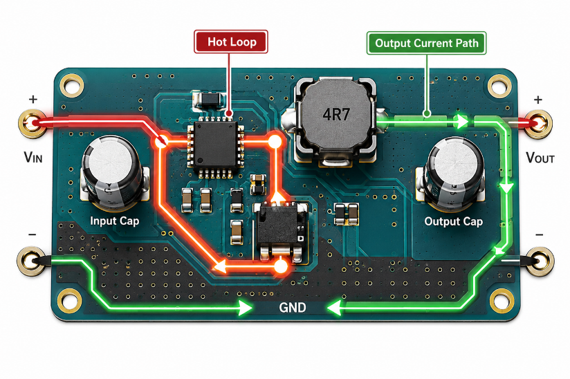
How Should the Buck Converter PCB Layout Control Current Path and Hot Loop?
The buck converter PCB layout should keep the switching current path short, direct and compact. The hot loop usually includes the input capacitor, high-side switch and low-side switch or diode. This loop carries fast current pulses, so even a small layout mistake can create ringing, EMI and unstable output.
- Place the input ceramic capacitor first: The input capacitor should be located next to the VIN and PGND pins of the switching IC or MOSFET stage. This is the most important placement rule because it closes the fastest current loop.
- Minimize the hot loop area: The input capacitor, switching device and return path should form the smallest practical loop. Long traces or separated ground returns increase parasitic inductance and can create voltage spikes.
- Keep the SW node short and controlled: The SW node connects the switch and inductor. It should be wide enough for current, but not enlarged unnecessarily. Large SW copper can behave like an antenna and increase radiated noise.
- Route current in a clear direction: Input current, switching current and output current should not cross sensitive signal areas. A clear current path makes the layout easier to inspect and reduces unexpected return current problems.
- Keep the output capacitor return path short: Output capacitors should return to power ground with low impedance. A long return path can increase ripple and reduce transient response performance.
- Separate feedback from noisy copper: Feedback, compensation, enable and soft-start traces should not pass under or beside the SW node, inductor or hot loop. These traces should be routed in a quiet area and connected close to the output sense point.
- Use vias carefully in power paths: Multiple vias are often needed when current moves between layers. Too few vias can create resistance, heat and voltage drop. Thermal vias should be placed under exposed pads when heat must move to inner or bottom copper.
- Avoid splitting the return path: Ground cuts, narrow necks or poorly placed slots can force current to take a longer path. This increases loop area and noise. The return path should stay directly under or close to the forward current path when possible.
- Reserve test and tuning positions: Test points for VIN, VOUT, GND, EN, FB and SW help prototype debugging. Optional snubber or filter pads can also help tune ringing and EMI after the first sample test.
How to Reduce EMI, Ripple and Noise in Buck Converter PCB Layout?
EMI, ripple and noise are often caused by layout, not only by the schematic. A buck converter may pass voltage testing but still fail radiated emission, conducted emission or ripple requirements if component placement, grounding and switching loop control are weak.
- Use the datasheet reference layout as the starting point: Most switching IC suppliers provide a tested layout example. The board can be adjusted for size and layer count, but the input capacitor position, SW node shape and ground return should not be changed casually.
- Place high-frequency capacitors closest to the IC: Small ceramic capacitors should be closest to VIN and PGND. Bulk capacitors can be placed slightly farther away. This layout order helps suppress fast switching noise before it spreads across the board.
- Keep noisy and quiet areas separated: The SW node, inductor, diode and MOSFET area should be treated as noisy. Feedback, sensing, clock, reset and analog circuits should be kept away from these areas.
- Control the SW node copper size: The SW node should not be poured as a large copper area unless thermal or current requirements truly need it. Smaller SW copper usually helps reduce parasitic capacitance and radiated EMI.
- Use a continuous ground plane when possible: A solid ground plane reduces impedance, improves return current flow and helps shield sensitive traces. For 4-layer boards, placing a ground layer close to the top power layer is usually helpful.
- Avoid routing feedback under the inductor: The magnetic field around the inductor and the switching voltage near the SW node can couple noise into feedback traces. Feedback should be routed on a quiet layer or away from the power stage.
- Control output ripple with both components and layout: Output capacitor value, ESR, ripple current rating and placement all matter. The capacitor must have a short connection to the load path and power ground to reduce ripple effectively.
- Use snubber or damping options for high-speed switching: If ringing appears on the SW node, an RC snubber or gate resistor adjustment may be needed. Reserving pads during layout gives more tuning flexibility during prototype testing.
- Keep high-current loops away from board edges: Switching loops near the board edge may radiate more easily. If space allows, keep the power stage compact and slightly inward from the edge.
- Validate noise under real working conditions: EMI and ripple should be checked at rated load, peak load, high input voltage, startup and load transient. A converter that looks clean at light load may show noise problems when current increases.
What Copper Thickness, Trace Width and Via Design Are Needed for Buck Converter PCB?
Copper thickness, trace width and via quantity depend on current, temperature rise, board thickness, copper layer, cooling method and layout space. A low-current buck converter board may use standard 1oz copper, while high-current designs may need 2oz, 3oz or heavier copper.
| Parameter | Common Value |
|---|---|
| 1oz copper | 35µm |
| 2oz copper | 70µm |
| 3oz copper | 105µm |
| Standard trace spacing | 4–6mil+ |
| Power trace spacing | Based on voltage and process |
| Finished via hole | 0.20–0.50mm |
| Thermal via pitch | 0.8–1.5mm |
| High-Tg FR-4 | Tg 170°C+ |
| Current margin | 20%–30% recommended |
For a buck converter circuit board, trace width should not be estimated by current alone. The copper area, airflow, nearby hot parts and allowed temperature rise must also be checked.
How Can Prototyping Reduce Buck Converter Power Module Risk?
Buck converter PCB prototype builds help verify layout, heat, ripple, output stability and assembly process before mass production. Prototype testing is especially important when the design has high current, compact space, strict EMI limits or wide input voltage.
A good prototype process starts with Gerber, BOM and datasheet layout review. Then the board is fabricated with the intended copper thickness, surface finish and stack-up. After assembly, the prototype is tested under light load, rated load, transient load and thermal stress.
Prototype checks should cover:
- Output voltage accuracy
- Ripple and noise
- Startup behavior
- Thermal rise at full load
- Inductor saturation risk
- Switching waveform
- Load transient response
- Connector and solder joint strength
- Basic EMI risk before certification
Prototype validation helps prevent layout mistakes from entering batch production.
What Should Be Checked Before Buck Converter PCB Assembly?
Buck converter PCB assembly should be checked from both electrical and manufacturing angles. Power components often have large pads, thermal pads, polarity direction and strict solder volume requirements, so SMT process control matters.
Before assembly, EBest Circuit checks:
- BOM accuracy: IC, MOSFET, diode, inductor, capacitors and resistor values.
- Polarity direction: diode, electrolytic capacitor, tantalum capacitor and IC orientation.
- Footprint match: pad size, thermal pad, exposed pad and package outline.
- Stencil opening: solder paste volume for thermal pads and power parts.
- Component spacing: clearance for rework, heat and inspection.
- Thermal balance: copper area and pad design for solderability.
- Test points: input, output, ground, feedback and enable pins.
For converter assembly, a small footprint error can cause poor soldering, heat concentration or unstable power output.
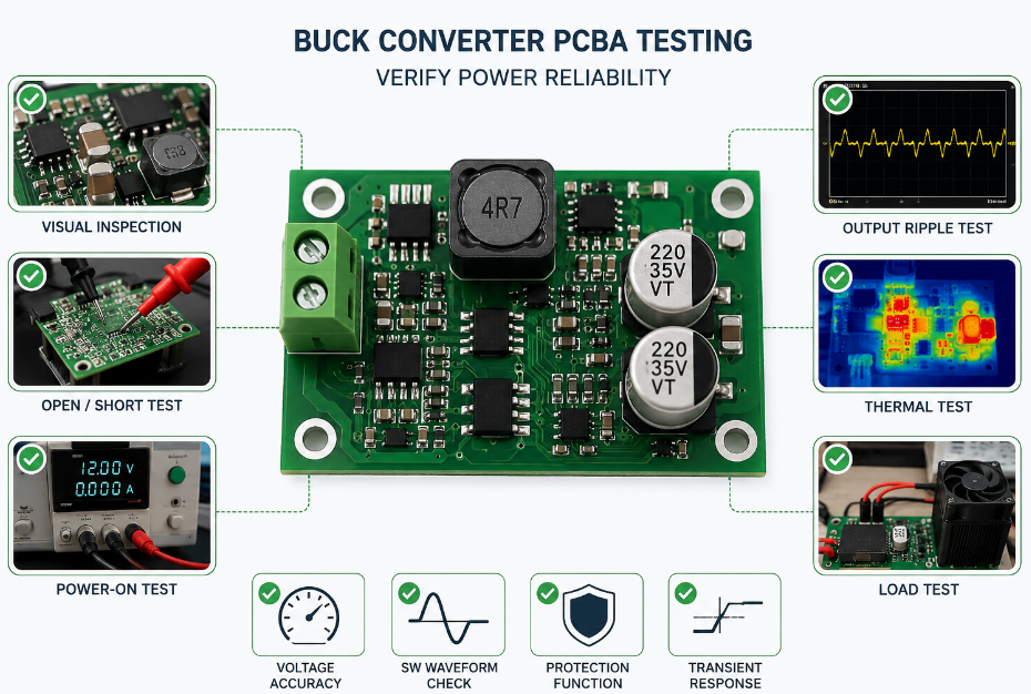
How Should Buck Converter PCBA Testing Verify Power Reliability?
Buck converter PCBA testing should prove that the assembled board can work safely under real load, temperature and switching conditions. Visual inspection is only the first step. Power reliability must be verified through electrical testing, waveform checking, load testing and thermal inspection.
- Check component placement and polarity first: AOI should confirm IC direction, diode polarity, capacitor polarity, inductor placement, missing parts, tombstoning and solder bridges. Polarity errors can damage the board immediately during power-on.
- Inspect solder joints on power components: MOSFETs, inductors, diodes, connectors and exposed-pad ICs often carry higher current or heat. Poor solder volume, voiding or cold solder joints can cause heat rise and intermittent failure.
- Run open and short testing before power-on: Flying probe or ICT should verify key nets before applying power. This reduces the risk of damaging ICs due to solder bridges, wrong resistor values or open feedback paths.
- Use current-limited startup testing: The first power-on should use a current-limited supply. VIN, VOUT, EN and standby current should be checked before full load is applied. Abnormal current draw may indicate short circuit, wrong component value or assembly error.
- Measure output voltage accuracy: Output voltage should be checked at no load, light load and rated load. Large deviation may indicate feedback resistor error, poor sensing location, unstable control loop or wrong BOM value.
- Check output ripple with an oscilloscope: Ripple should be measured with proper probe grounding. Long probe ground leads can create false noise readings. Ripple should be checked at rated current and high input voltage.
- Review SW node waveform: Excessive ringing, overshoot or abnormal duty behavior may point to hot loop inductance, poor grounding, wrong snubber design or layout-related switching noise.
- Perform rated load and peak load testing: The assembled board should operate at rated current for enough time to reach thermal stability. Peak load testing helps confirm current margin, inductor behavior and protection response.
- Measure thermal rise on key parts: The switching IC, MOSFET, diode, inductor, output capacitor and connector should be checked with a thermal camera or contact measurement. Hot spots should be reviewed before batch production.
- Test load transient response: Fast current changes should not cause excessive voltage dip, overshoot or oscillation. This test is important for motors, communication modules, embedded processors and pulsed-load systems.
- Verify protection functions: Overcurrent, short-circuit, thermal shutdown, undervoltage lockout and enable control should be tested if the design supports them. Protection testing helps reduce field failure risk.
- Confirm final functional performance: The final test should match the actual product use, including input voltage range, output load, connector function, control signals and customer-defined acceptance criteria.
Buck Converter PCB Case Study: From Prototype to Mass Production
Before mass production, many buck converter PCB problems are not found in the schematic, but appear during prototype testing, load testing or assembly verification. The following project case shows how EBest Circuit helped a customer find layout, thermal and testing risks early, then improve the design from prototype review to pilot production.
Project background:
A customer developed a compact buck converter board for an industrial control product. The first prototype could power on, but the output ripple was unstable under load, and the switching IC area became hot after continuous operation.
Project requirements:
The customer needed stable voltage output, lower ripple, better heat control and reliable assembly quality. They also wanted one supplier to support DFM review, PCB prototype, component sourcing, assembly and testing before mass production.
Our solution:
EBest Circuit reviewed the schematic, Gerber files, BOM, copper thickness, hot loop, SW node, input capacitor position, feedback routing and thermal vias. We helped improve the input loop, copper heat spreading, feedback path and test point design. During assembly, we controlled solder paste, component polarity and power component soldering quality.
Output result:
The updated prototype showed more stable output, better heat distribution and easier waveform testing. After AOI, flying probe testing, power-on testing, ripple review and load testing, the project moved into pilot production with clearer inspection standards and lower redesign risk.
What Buck Converter PCB Services Can EBest Circuit Provide?
The case above shows that buck converter PCB reliability depends on design review, fabrication, assembly and testing working together. EBest Circuit provides one-stop support for buck converter PCB projects, helping customers reduce supplier communication, shorten development time and improve production control.
- PCB design review:
Check Gerber files, stack-up, copper thickness, hot loop, SW node, feedback routing, thermal vias and test points before fabrication. - PCB prototype:
Support prototype production and quick-turn PCBA so customers can test ripple, heat, output voltage and load stability early. - PCB fabrication:
Support FR-4 PCB, multilayer PCB, high-Tg PCB, heavy copper PCB, metal core PCB, ceramic PCB, flexible PCB, rigid-flex PCB, HDI PCB and impedance control PCB. - Component sourcing:
Help source SMD, BGA, QFN, QFP and other components, reducing BOM shortage risk and unexpected purchasing delays. - PCB assembly:
Support SMT, THT and mixed assembly for buck converter boards with MOSFETs, inductors, diodes, ICs, connectors and exposed-pad components. - Testing and inspection:
Provide AOI, flying probe testing, power-on testing, ripple checking, thermal review and functional testing before shipment. - Mass production support:
Support prototype, low-volume production and repeat batch orders, helping customers move from sample approval to stable supply. - Global project compliance:
Support projects requiring ISO 9001, IATF 16949, ISO 13485, AS9100D, UL, RoHS and REACH.
Why Choose EBest Circuit for Custom Buck Converter PCB Projects?
Beyond basic PCB and PCBA services, customers choose EBest Circuit because we help reduce redesign risk, shorten prototype cycles and make batch production easier to control. For custom buck converter PCB projects, this means fewer supplier handover problems and more stable power board delivery.
- Reduce redesign risk before fabrication:
We check Gerber files, BOM, stack-up, copper thickness, hot loop area, SW node, feedback routing and thermal vias before production. This helps find layout risks early instead of fixing problems after assembly. - Save communication time:
You do not need to coordinate separate PCB, component and assembly suppliers. EBest Circuit provides PCB fabrication, component sourcing, SMT assembly, through-hole assembly, mixed assembly and testing, making project management easier. - Improve prototype speed:
For new buck converter projects, fast samples help you test voltage output, ripple, heat and load stability earlier. Our prototype and quick-turn PCBA support helps shorten the path from design verification to pilot run. - Control component cost and shortage risk:
Power projects often face BOM changes, unavailable ICs or capacitor replacement issues. Our sourcing team helps check component availability, alternatives and cost before production, reducing unexpected delays. - Improve assembly reliability:
Buck converter assemblies often include MOSFETs, inductors, diodes, exposed-pad ICs and connectors. We control solder paste, polarity, component placement and inspection to reduce solder defects, overheating and unstable output. - Support compact and complex PCBA:
EBest Circuit supports SMT, THT and mixed assembly, 01005 components and 0.25mm BGA pitch. This helps customers build compact power boards with better assembly control. - Verify quality before shipment:
AOI, flying probe testing, power-on testing, thermal checking, ripple review and functional testing help confirm whether the board can work under real operating conditions before delivery. - Support stable repeat production:
With 20+ years PCB experience and monthly PCB capability of 260,000 square feet, EBest Circuit can support prototype, low-volume production and repeat orders, helping customers move from sample approval to stable supply. - Meet global project requirements:
ISO 9001, IATF 16949, ISO 13485, AS9100D, UL, RoHS and REACH support industrial, automotive, medical, aerospace and export-oriented electronics projects.
EBest Circuit helps customers reduce design risk, shorten development time, control production cost and improve power board reliability. If you need custom buck converter PCB manufacturing, prototype or assembly, contact us for a fast quote: sales@bestpcbs.com.
What Files and Specifications Are Needed for a Fast Quote?
A fast buck converter PCB quote needs complete design and production files. Missing information can delay pricing, DFM review and assembly preparation.
Please prepare:
- Gerber files
- Drill files
- PCB stack-up
- Copper thickness
- Board thickness
- Surface finish
- BOM
- Pick-and-place file
- Assembly drawing
- Test requirements
- Target quantity
- Special packaging needs
- Input/output voltage and current
- Operating temperature range
For design review support, sending the schematic and datasheet reference layout can help us check current path, hot loop, feedback routing and thermal design more accurately.
FAQs About Buck Converter PCB
Q1: What files should I send for a quote?
A1: Please send Gerber files, drill files, BOM, pick-and-place file, assembly drawing, copper thickness, board thickness, surface finish, quantity and testing requirements. For power projects, input voltage, output voltage, output current and operating temperature are also helpful.
Q2: Can EBest Circuit review my layout before production?
A2: Yes. We can review the hot loop, SW node, input capacitor position, feedback routing, copper width, thermal vias and test points before fabrication. This helps find layout risks before they become assembly or testing problems.
Q3: Why does the prototype pass power-on testing but fail under load?
A3: Light-load testing cannot expose all risks. Under rated load, the board may show high ripple, voltage drop, inductor saturation, hot components or unstable feedback. Load testing and thermal checking are needed before pilot production.
Q4: Is a 2-layer buck converter board enough?
A4: A 2-layer board may work for low-current designs. For higher current, compact layout, stronger EMI control or better heat spreading, a 4-layer board with a solid ground plane is usually safer.
Q5: What causes high output ripple?
A5: High ripple may come from poor capacitor selection, long current paths, weak grounding, inductor saturation, large hot loop area or noisy feedback routing. Both schematic and PCB layout should be checked together.
Q6: How can EMI risk be reduced?
A6: Place input capacitors close to VIN and PGND, keep the hot loop compact, reduce SW node copper, protect feedback traces and reserve snubber or filter pads. Prototype testing should include ripple and waveform review.
Q7: What assembly risks should be checked?
A7: Common risks include wrong polarity, poor exposed-pad soldering, solder bridges, insufficient solder on power parts, connector solder cracks and component shift. AOI, solder paste control and electrical testing help reduce these problems.
Q8: Can EBest Circuit source components for my project?
A8: Yes. We support component sourcing for SMD, BGA, QFN, QFP and other electronic parts. This helps customers check availability, alternatives and cost before production, reducing BOM-related delays.
Q9: What tests are recommended before mass production?
A9: Recommended tests include AOI, flying probe testing, power-on testing, output voltage check, ripple measurement, SW waveform review, load testing, thermal inspection and final functional testing.
Q10: Can EBest Circuit support both prototype and batch production?
A10: Yes. We support PCB prototype, low-volume production and mass production. This helps keep design history, process control and testing requirements consistent from first sample to repeat orders.
Conclusion
A buck converter PCB should be reviewed as a complete power conversion board, not only as a simple circuit. Hot loop control, feedback routing, copper thickness, thermal vias, component selection, soldering quality and load testing all affect final reliability.
For purchasing decisions, choose a supplier that can support design review, prototype fabrication, component sourcing, PCB assembly, testing and stable batch production in one workflow. EBest Circuit provides custom buck converter PCB manufacturing and assembly support for global customers. Send your Gerber files, BOM and project requirements to sales@bestpcbs.com for a fast quote.