PCB manufacturing PCB manufacturing
Home > Blog

Automotive IR Illuminator Aluminum PCB for In-Cabin Sensing Systems

August 20th, 2026

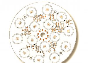
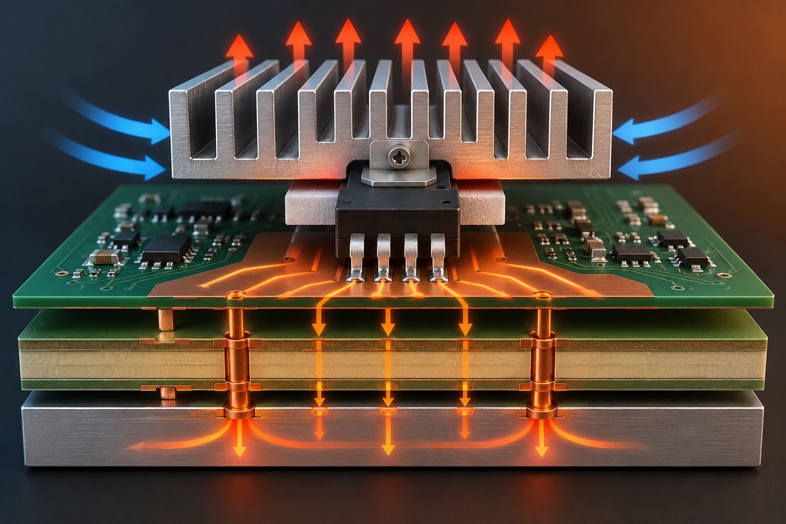
An automotive IR illuminator aluminum PCB carries current to infrared emitters, provides a stable mounting platform and transfers heat away from the LED array in driver monitoring and other in-cabin sensing systems. The PCB design has to work with the IR emitter package, current profile, camera field of view, beam pattern and module geometry.

Are you worried about these automotive IR illumination problems?

  • The IR LED array runs too hot during pulsed or continuous operation.
  • The camera sees uneven IR illumination, with bright and weak areas across the field of view.
  • The prototype works, but LED position, PCB construction or assembly quality becomes difficult to keep consistent in production.

As a professional one-stop PCB and PCBA service provider, EBest Circuit supports automotive IR illuminator aluminum PCB fabrication, component sourcing, PCB assembly, prototyping and mass production. Our solutions include:

  • Control Current and Heat Around the Emitters
    Match copper geometry, thermal dielectric and metal-core construction to the actual LED current and emitter layout.
  • Maintain Optical and Mechanical Alignment
    Control LED position, orientation, PCB dimensions and mounting features so the illuminator fits the camera module as designed.
  • Carry the Approved Build Into Production
    Keep the validated PCB construction and assembly requirements consistent when moving from prototypes to volume manufacturing.

For an automotive camera illumination aluminum PCB or in-cabin sensing IR aluminum PCB, send your Gerber files, IR LED datasheet and project requirements to sales@bestpcbs.com for a quotation.

Automotive IR Illuminator Aluminum PCB, https://www.bestpcbs.com/blog/2026/08/automotive-ir-illuminator-aluminum-pcb/

What Is an Automotive IR Illuminator Aluminum PCB and Where Is It Used in In-Cabin Sensing?

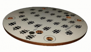
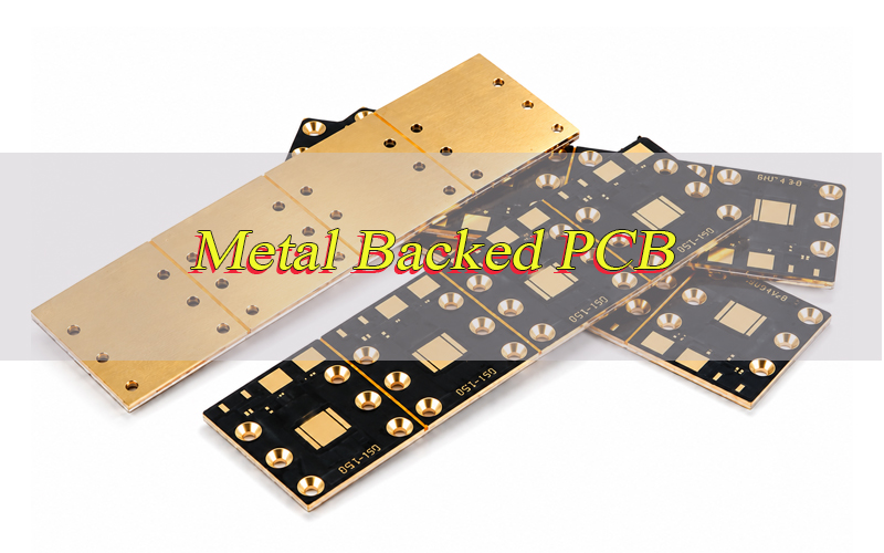
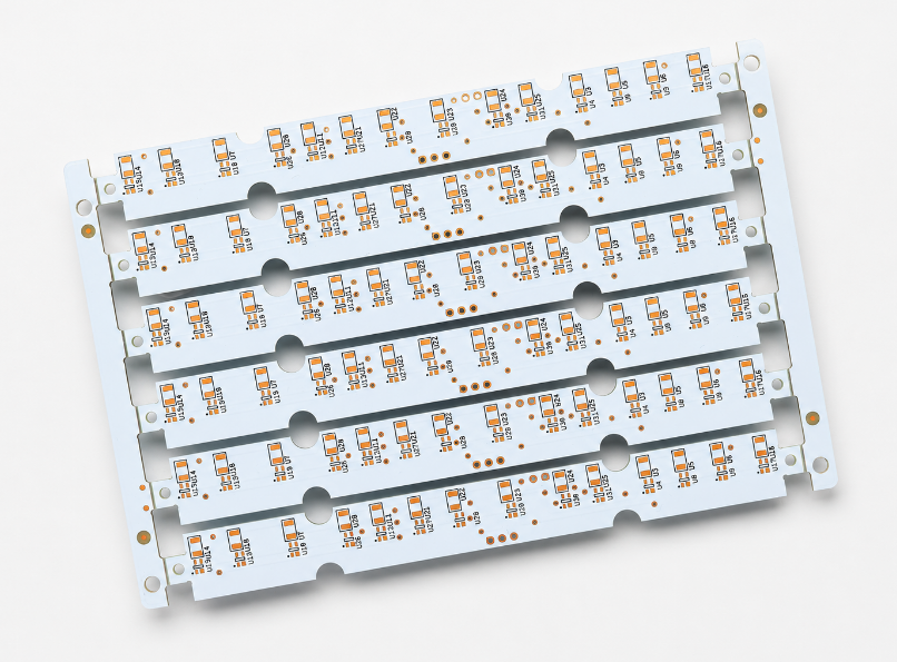
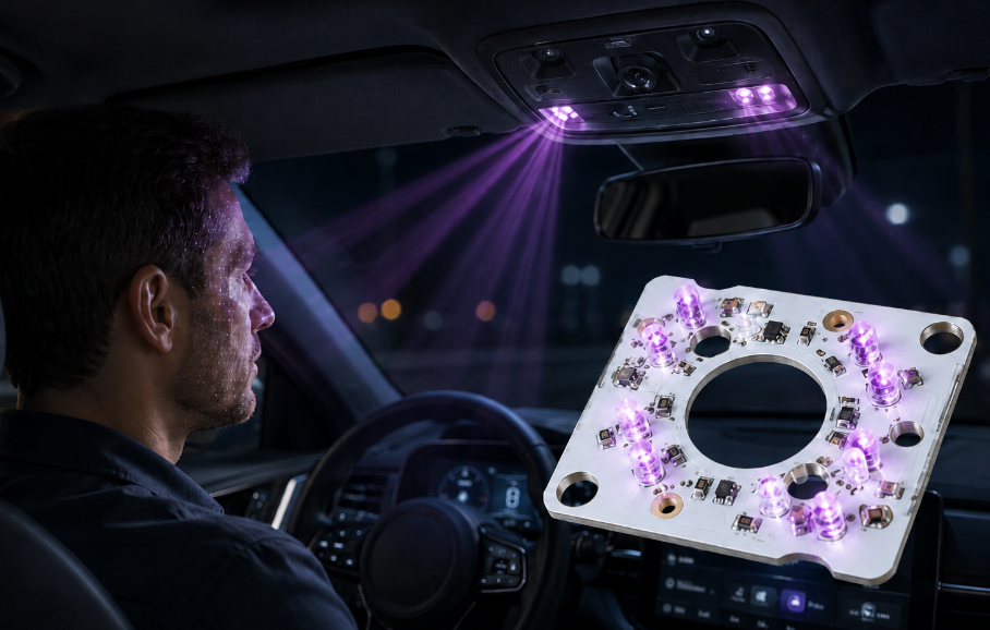
An automotive IR illuminator aluminum PCB is a metal-based PCB used to mount and power infrared LEDs in automotive camera and in-cabin sensing modules. Its main functions are to carry LED current, hold the emitters in the required positions and transfer heat away from the IR LED array.

The board is part of the sensing module rather than a stand-alone lighting circuit. IR LED position, beam direction, camera location and housing geometry all affect how the illuminator performs after installation.

Depending on the optical design, the module may use 850 nm or 940 nm IR emitters.

Typical applications include:

  • Driver Monitoring Systems (DMS): Supports imaging of the driver’s face, eyes and head position.
  • Occupant Monitoring Systems (OMS): Provides IR illumination across passenger and seating areas.
  • Child Presence Detection: Supports camera-based sensing in low visible-light conditions.
  • Interior and Gesture Monitoring: Used in overhead consoles, displays and interior camera modules.
  • Eye-Tracking Systems: Provides controlled illumination around the driver’s eyes and facial area.
Automotive IR Illuminator Aluminum PCB, https://www.bestpcbs.com/blog/2026/08/automotive-ir-illuminator-aluminum-pcb/

How Should an In-Cabin Sensing IR Aluminum PCB Handle LED Current and Heat?

An in-cabin sensing IR aluminum PCB needs to be designed around the actual LED current waveform, particularly when the emitters operate in pulsed or strobed modes.

Average current alone does not describe the load on the PCB. During a high-current pulse, the traces, pads, connectors and solder joints may carry a much higher instantaneous current.

  • Size Current Paths for Peak Current
    Use the actual pulse current when setting trace width and copper area. Narrow conductors increase resistance, voltage drop and localized heating.
  • Keep High-Current Paths Short
    Reduce unnecessary distance between the IR LED driver and emitter array. Shorter paths lower resistive loss and make current delivery easier to control.
  • Provide Enough Copper Around the Emitters
    Adequate copper supports current carrying and helps spread heat away from concentrated emitter areas.
  • Avoid Excessive Emitter Clustering
    Several high-current IR LEDs placed in a small area can create a localized thermal load. Their spacing needs to work for both optical coverage and heat distribution.
  • Include Driver Losses When the Driver Shares the PCB
    If the driver is mounted on the same automotive IR LED PCB, its losses become part of the total thermal load.
  • Define the Pulse Profile
    Provide peak current, pulse width and duty cycle during PCB review. These values describe the operating condition more accurately than a single nominal wattage.

How Should Automotive IR LED PCB Layout Support Camera Alignment and Uniform Illumination?

An automotive IR LED PCB layout needs to match the camera field of view and the required illuminated area. LED position, spacing, orientation and beam direction can all affect the image captured by the camera.

  • Match the IR Beam to the Camera Field of View
    A narrow beam may leave weak areas near the edges of the image. A beam that is too wide sends part of the IR output outside the useful sensing region.
  • Control IR LED Orientation
    Directional or asymmetric emitters need the correct rotation on the PCB. A component can be electrically correct and still illuminate the wrong area.
  • Distribute Emitters Across the Required Region
    Poor spacing can create excessive intensity in one area while leaving other parts of the camera image under-illuminated.
  • Use Stable Mechanical References
    Mounting holes, board edges and locating features need to match the camera or illuminator housing so the same optical alignment can be reproduced during assembly.
  • Keep the Optical Path Clear
    Screws, connectors, shields and tall components should not interfere with the IR beam.
  • Include Secondary Optics in the Mechanical Layout
    When the module uses lenses, light guides, diffusers or optical windows, their position and tolerances need to be coordinated with the PCB.

How Should Temperature, Vibration and Long Operating Cycles Affect Automotive IR PCB Design?

Automotive IR modules can experience repeated temperature changes, vibration and high-current emitter pulsing. These conditions affect solder joints, mounting features and the long-term stability of the PCB assembly.

  • Operating Temperature
    PCB materials, solder mask, surface finish and assembly materials need to suit the intended module environment.
  • Thermal Cycling
    Repeated heating and cooling places mechanical stress on solder joints and interfaces around high-current emitters.
  • PCB Mechanical Support
    Large connectors and unsupported board sections should not transfer unnecessary mechanical load to the IR LED solder joints.
  • Mounting-Hole Accuracy
    The PCB should fit the housing without being forced or bent during installation. Poor hole positioning can introduce mechanical stress into the finished module.
  • Component Retention
    Larger components and connectors may require additional mechanical support where vibration is expected.
  • Repeated Pulsed Operation
    High-current strobing creates recurring electrical and thermal loading. The current path and solder joints need to remain stable under the intended operating profile.

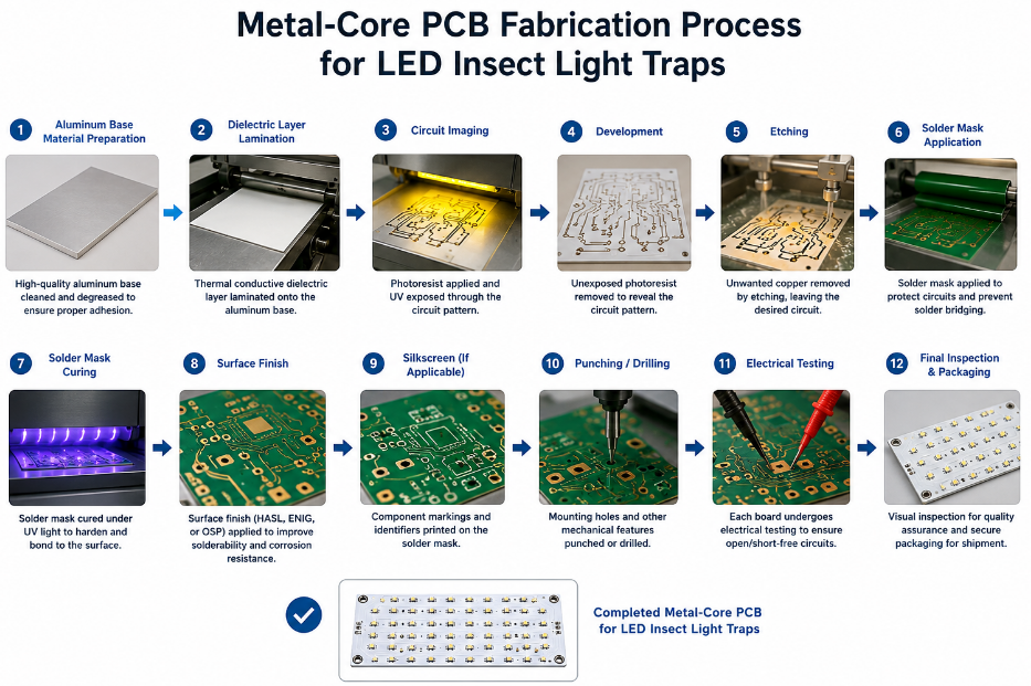
What Steps Are Used to Manufacture and Assemble an Automotive IR Illuminator Aluminum PCB?

An automotive IR illuminator aluminum PCB requires controlled fabrication and assembly so the emitter positions, current paths and approved metal-core construction remain consistent.

Step 1: Review the Design and IR LED Requirements

Check the IR LED part number, wavelength, footprint, polarity, orientation, peak current, copper weight, PCB thickness, thermal dielectric, mounting features and surface finish before production starts.

Step 2: Prepare the Metal-Core Laminate

Use the approved copper, dielectric and aluminum construction. A material change can affect thermal performance, finished thickness and mechanical fit.

Step 3: Form the Copper Circuit

Image and etch the IR LED pads, high-current paths and supporting circuitry. Trace width and spacing need to remain compatible with the selected copper weight.

Step 4: Drill and Profile the PCB

Produce mounting holes, slots and the finished board outline from the mechanical drawing. These features may directly control the position of the illuminator inside the camera housing.

Step 5: Apply Solder Mask and Surface Finish

Keep IR LED pads and other solderable areas correctly exposed. The selected surface finish needs to suit the component package and assembly process.

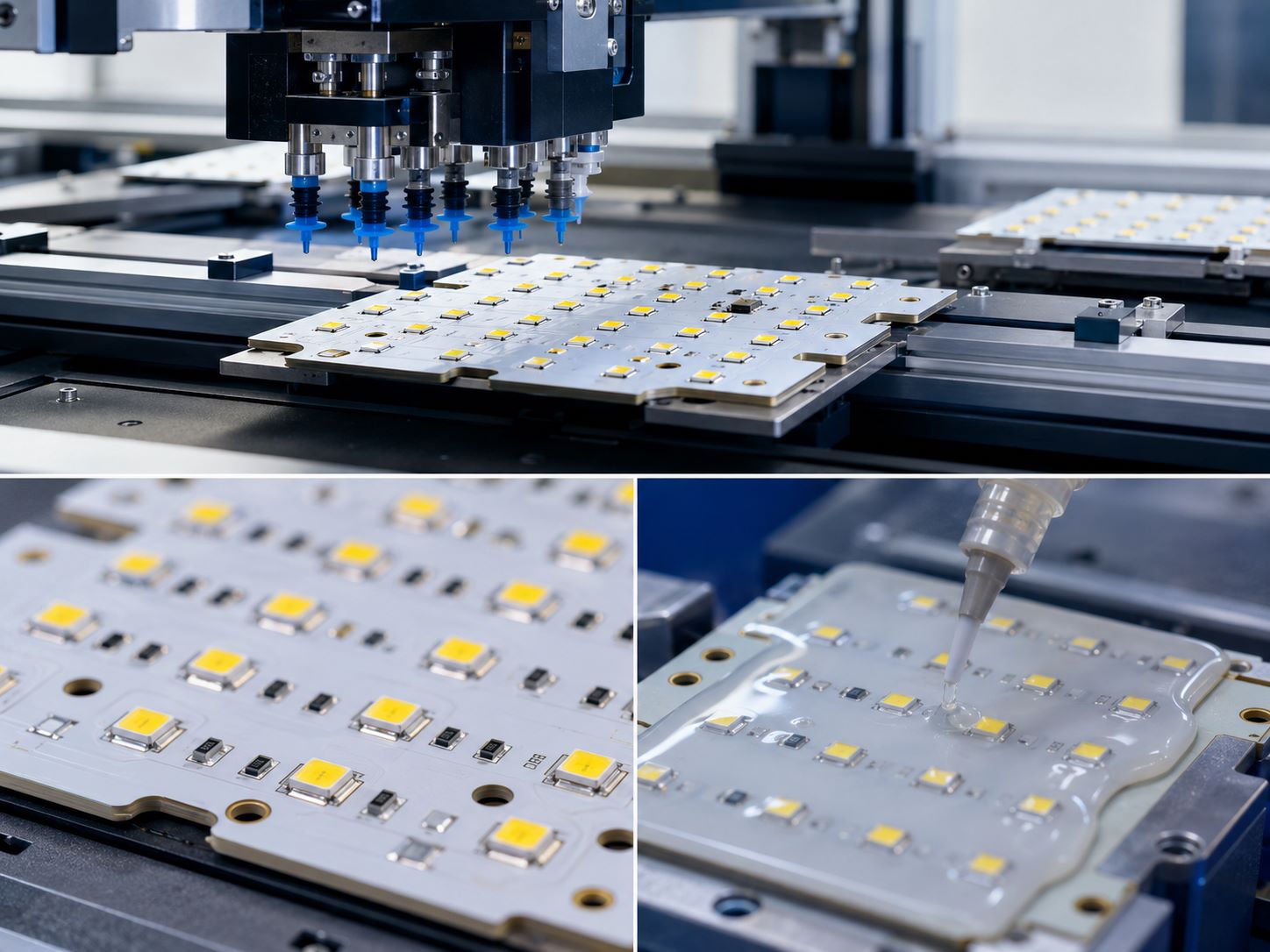
Step 6: Print Solder Paste

Match stencil openings and solder-paste volume to the IR LED package. Poor paste control can lead to uneven package seating after reflow.

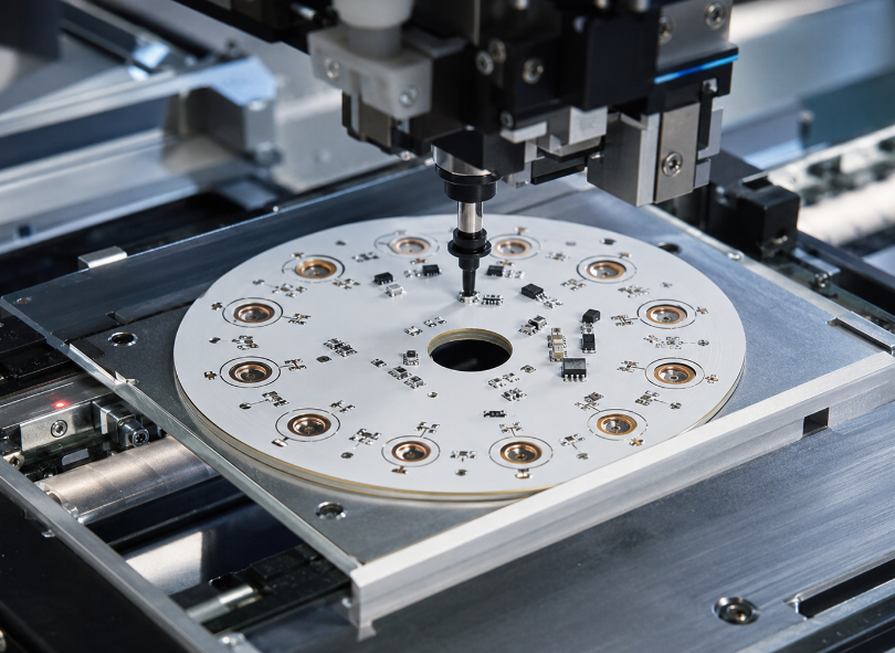
Step 7: Place the IR LEDs

Control X/Y location and component rotation. Placement accuracy is especially important for directional or asymmetric emitters.

Step 8: Complete Reflow Soldering

Use a reflow profile suitable for the selected components. After soldering, check for poor wetting, package tilt, insufficient solder and other visible defects.

Step 9: Verify the Finished Assembly

Check IR LED polarity, electrical operation, current behavior and mechanical fit before the assembly moves to the next production stage.
Automotive IR Illuminator Aluminum PCB Manufacturing, https://www.bestpcbs.com/blog/2026/08/automotive-ir-illuminator-aluminum-pcb/

What Steps Are Used to Inspect and Test Automotive IR Illuminator PCBs?

Inspection should concentrate on the characteristics that can affect current delivery, IR LED alignment, thermal transfer and final module operation.

Step 1: Verify PCB Construction

Check the aluminum base, thermal dielectric, copper thickness and finished PCB thickness against the approved build.

Step 2: Check Critical Dimensions

Inspect the board outline, mounting holes, slots and locating features used to position the illuminator inside the module.

Step 3: Inspect Circuit and Surface Quality

Use visual inspection and AOI where applicable to identify opens, shorts, damaged pads, contamination and solder-mask defects.

Step 4: Perform Electrical and Insulation Testing

Verify circuit continuity and electrical isolation between the conductive circuit and metal base.

Step 5: Verify IR LED Placement

Check the emitter part number, polarity, X/Y position and rotation against the approved assembly data.

Step 6: Inspect Solder Joints

Review solder wetting and package seating. A tilted IR emitter can affect both heat transfer and beam direction.

Step 7: Perform Functional Current Testing

Operate the assembly under the defined electrical conditions and check LED switching, current delivery and supporting circuit operation.

Step 8: Check Thermal Performance

For higher-current arrays, test the PCB under representative operating conditions. Pulsed designs need an appropriate peak current and duty cycle during validation.

Step 9: Verify Optical Output When Required

When the project includes optical acceptance criteria, test the illuminator using the specified camera, IR sensor or optical fixture rather than relying on visual inspection.
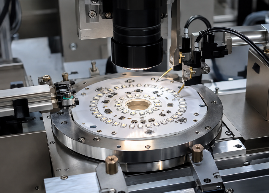
Automotive IR Illuminator Aluminum PCB Testing, https://www.bestpcbs.com/blog/2026/08/automotive-ir-illuminator-aluminum-pcb/

What Automotive IR Aluminum PCB Manufacturing Capabilities Can We Provide?

The table below summarizes our main MCPCB manufacturing capabilities for automotive IR illuminator PCB projects.

ItemCapabilities
Maximum Layer CountUp to 10 layers
PCB Thickness0.3–4.0 mm
Maximum Board SizeUp to 610 × 1220 mm (24 × 48 in.)
Copper Weight0.5–10 oz
Minimum Trace / Space0.15 / 0.15 mm (6 / 6 mil)
Minimum Hole Diameter0.30 mm (12 mil)
Minimum Punch Hole Diameter3.0 mm (0.12 in.)
Minimum Hole Spacing0.40 mm (16 mil)
Maximum Aspect Ratio12:1
Minimum Solder Pad Diameter0.40 mm (16 mil)
Thermal Conductivity0.8–1.5 W/m·K standard; 2.0–6.0 W/m·K high thermal conductivity
Warp and Twist< 0.75%
FlammabilityUL 94V-0
Thermal Stress6 × 10 sec at 288°C
Surface FinishENIG, Flash Gold, Hard Gold, Selective Gold Plating, HASL, Lead-Free HASL, OSP, Immersion Silver, Immersion Tin

Case Study: Automotive IR Illuminator Aluminum PCB From Prototype to Production

Project Background

An in-cabin camera module required a compact automotive IR illuminator aluminum PCB for a high-current IR emitter array. The PCB had to fit the camera-module housing while holding the emitters in the positions defined by the optical design.

Project Requirements

The PCB needed to:

  • Carry the specified pulsed LED current
  • Keep IR emitter position and polarity consistent
  • Transfer heat into the metal substrate
  • Match the camera-module mounting geometry
  • Fit within the available module space
  • Support both prototype validation and repeat production

Our Solution

EBest Circuit reviewed the IR LED datasheet, PCB layout and mechanical drawing before prototype fabrication.

The project focused on:

  • Matching IR LED footprints and package orientation
  • Reviewing copper weight and high-current trace geometry
  • Selecting the required thermal dielectric and aluminum construction
  • Controlling board outline and mounting-hole positions
  • Maintaining IR LED placement accuracy during assembly
  • Checking LED seating and solder joints after reflow
  • Keeping the validated PCB construction unchanged for production

Results

Prototype validation confirmed:

  • Correct IR LED placement and polarity
  • Stable mechanical fit inside the camera module
  • Controlled current paths for the emitter array
  • Consistent heat transfer into the metal base
  • A repeatable PCB and assembly specification for production

What Files and Specifications Are Required for an Automotive IR Illuminator Aluminum PCB Quote?

For an automotive IR illuminator aluminum PCB quote, provide the available PCB files, assembly data and key IR LED requirements.

PCB Fabrication:

  • Gerber files
  • NC drill files
  • Mechanical drawing
  • PCB dimensions and thickness
  • Copper weight
  • Aluminum thickness
  • Thermal conductivity requirement
  • Surface finish
  • Quantity and special tolerances

PCB Assembly:

  • BOM
  • Pick-and-place file
  • Assembly drawing
  • IR LED part number and datasheet
  • Polarity and orientation requirements
  • Functional-test requirements

IR and System Requirements:

  • IR wavelength, such as 850 nm or 940 nm
  • Continuous or pulse current
  • Pulse width and duty cycle
  • Number of IR emitters
  • IR LED beam angle
  • Camera field of view
  • Operating temperature
  • Optical acceptance requirements, if applicable

If some specifications are still open, send the available project files first for review.

Why Choose EBest Circuit for Automotive IR LED PCB Manufacturing?

EBest Circuit has more than 20 years of PCB manufacturing experience and supports projects from prototype fabrication to component sourcing, PCB assembly and mass production. Metal-based PCB / MCPCB is included in our PCB product range.

  • Reduce Supplier Coordination
    Keep PCB prototyping, MCPCB fabrication, component sourcing and PCB assembly within one project instead of managing several separate suppliers. This simplifies communication when the IR LED, PCB and assembly requirements need to be reviewed together.
  • Keep Prototype and Production Builds Consistent
    The approved PCB construction, IR LED orientation and assembly requirements can stay within the same manufacturing route as the project moves from engineering samples to volume production, reducing unnecessary changes between stages.
  • Support Automotive Project Requirements
    EBest Circuit holds IATF 16949, together with ISO 9001:2015, ISO 13485:2016 and AS9100D, providing an established quality-management framework for projects with different industry requirements.
  • Handle Thermal PCB Requirements in One Manufacturing Source
    Because metal-based PCB / MCPCB is part of our PCB manufacturing range, automotive IR illuminator projects can be reviewed and produced without moving the thermal PCB portion to a separate supplier.
  • Scale From Engineering Samples to Ongoing Production
    EBest Circuit has approximately 260,000 sq. ft. (28,900 m²) of monthly PCB manufacturing capability and completes more than 1,000 different boards, supporting both prototype programs and continuing production demand.
  • Shorten Lead Time for Eligible Urgent Builds
    Expedited service is available for qualifying projects, with eligible urgent boards capable of shipment within 24 hours. Final lead time depends on the PCB construction and project requirements.

For an automotive IR illuminator aluminum PCB used in DMS, OMS or another in-cabin sensing system, send your Gerber files, BOM, IR LED datasheet and mechanical drawing to sales@bestpcbs.com for a quotation.

FAQs About Automotive IR Illuminator Aluminum PCBs

Q1: Should high-power automotive IR LEDs use a constant-current driver?
A1: In most high-power designs, yes. Controlled current provides more predictable emitter output and prevents excessive LED current. The operating point should follow the selected IR LED and driver specifications.

Q2: Why are IR LEDs often operated in pulsed mode in DMS modules?
A2: Pulsed operation allows the illumination period to be coordinated with camera exposure while reducing average power compared with continuous operation. The PCB still needs to carry the full peak current during every pulse.

Q3: Is 940 nm completely invisible inside the vehicle?
A3: Not under every operating condition. 940 nm generally produces less visible red glow than 850 nm, which is one reason it is commonly considered for in-cabin sensing.

Q4: Can one IR illuminator PCB be used for both DMS and OMS?
A4: Yes, if the optical design covers both sensing regions. Emitter position, beam angle and camera field of view need to be designed together, rather than simply increasing the number of IR LEDs.

Q5: Can an IR illuminator aluminum PCB include connectors and temperature sensors?
A5: Yes. Connectors, thermistors or other monitoring components can be integrated when routing space and assembly requirements allow. Their location should not interfere with the IR optical path.

Q6: Can FR4 be used for an automotive IR emitter array?
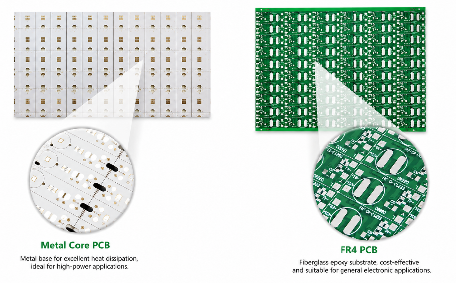
A6: It can be suitable for lower thermal loads. A metal-core PCB becomes more useful when multiple high-current IR emitters concentrate heat in a limited board area.

Q7: Does IR emitter binning matter when sourcing components?
A7: It can. Radiant output, wavelength and electrical characteristics may vary by bin or part specification. If the optical design depends on a defined emitter range, the approved sourcing specification should identify it clearly.

Q8: Can near-infrared output be checked visually during production?
A8: No. Visible appearance is not a reliable measurement of near-infrared radiant output. Use an IR-sensitive camera, photodetector or defined optical test fixture when optical verification is required.

Q9: Should the optical window be included during final illumination testing?
A9: Yes when it is part of the finished optical path. Window material, coating, geometry and position can affect the IR energy reaching the camera or sensing area.

Q10: What information should be controlled after prototype approval?
A10: Keep the approved IR LED part number, package orientation, PCB construction, mechanical references and assembly requirements under revision control so production builds remain consistent with the validated design.

Conclusion

An automotive IR illuminator aluminum PCB has to carry high-current IR emitter loads while keeping LED position, mechanical fit and thermal performance consistent inside the sensing module. Current routing, emitter placement, mounting accuracy and assembly control all influence the final result.

EBest Circuit supports metal-core PCB manufacturing, prototyping, component sourcing, PCB assembly and mass production. For an automotive camera illumination aluminum PCB, in-cabin sensing IR aluminum PCB or automotive IR LED module, send your project files and requirements to sales@bestpcbs.com for a quotation.
You may also like

Top 10 Aluminum PCB Manufacturers in China (2026)

August 20th, 2026

Finding an aluminum PCB manufacturer in China is not difficult. The harder part is finding one whose material options, copper capability, thermal design support, mechanical tolerances, production model, and PCB assembly services actually match your project. A factory that is ideal for a standardized LED prototype may not be the right choice for a thick-copper power board, a multilayer aluminum PCB, or an OEM project moving directly into PCBA production.

This guide compares ten aluminum PCB manufacturers in China from a practical engineering and sourcing perspective. Rather than looking only at company size, the comparison focuses on what each supplier is better suited to manufacture and what you should check before releasing Gerber files or selecting a long-term production partner.

aluminum PCB manufacturer

How We Selected the Top Aluminum PCB Manufacturers in China

A manufacturer should offer more than a page saying that aluminum PCBs are available. The useful differences appear in actual materials, board structures, manufacturing limits, engineering support, quality control, and the ability to move from prototype into repeat production.

The manufacturers below were considered around several practical factors:

  • Aluminum PCB manufacturing experience
  • Available board structures and materials
  • Prototype and production support
  • Engineering and DFM support
  • PCB assembly capability
  • Quality and process control
  • Support for international projects

No single supplier is the best fit for every aluminum circuit board. The right choice depends on where your design is most demanding.

Top 10 Aluminum PCB Manufacturers in China

The table below provides a quick shortlist before looking at each supplier in more detail.

No.ManufacturerBest For
1PCBWayOnline prototyping
2JLCPCBStandard low-cost builds
3ALLPCBOnline PCB + PCBA
4EBest CircuitCustom thermal PCB + PCBA
5PCBasicPrototype to production
6Viasion TechnologyLow-/mid-volume builds
7RayMing TechnologyCustom PCB + assembly
8Hitech CircuitsLED / thermal PCB
9Venture ElectronicsMultilayer metal-core PCB
10WellPCBPCB + assembly

1. PCBWay

  • PCBWay is a widely used China-based PCB manufacturing platform with a dedicated aluminum PCB service alongside rigid, flex, rigid-flex, HDI, heavy-copper, metal-core, and other PCB technologies. Its online quotation model makes it particularly accessible during prototype development, where engineers want to upload files, select manufacturing parameters, and move quickly into a small build.
  • The company also publishes information on different aluminum PCB structures, including multilayer constructions, rather than limiting the service to conventional one-layer LED boards. PCB assembly is available when the project needs to move beyond bare-board fabrication.

Best for: Engineers who prefer an online ordering workflow and need flexible prototype or custom PCB options.

2. JLCPCB

  • JLCPCB is particularly attractive when the aluminum PCB fits a standardized manufacturing window. Its current metal-core PCB service includes aluminum- and copper-core options, while the published PCB capabilities identify one-layer aluminum-core boards as a supported material category.
  • That clear process boundary is useful for straightforward prototypes. Engineers can determine early whether the board fits the available material and fabrication options instead of spending time on an open-ended RFQ.
  • For more unusual structures, however, a supplier with a more engineering-led quotation process may be preferable.

Best for: Standardized aluminum PCB prototypes where online ordering and cost control are priorities.

3. ALLPCB

  • ALLPCB combines online PCB manufacturing with component sourcing and PCB assembly. Its current aluminum PCB capability covers 1–2 layers, multiple copper weights, several board thicknesses, and different thermal-conductivity options. The same platform also supports SMT, THT, inspection, X-ray, programming, and functional testing.
  • This makes ALLPCB relevant to buyers who want the convenience of an online sourcing model without necessarily stopping at the bare board.
  • The published process range is also useful for initial screening because engineers can compare their stackup and copper requirements against defined limits before ordering.

Best for: Online aluminum PCB sourcing with downstream PCB assembly requirements.

4. EBest Circuit

  • EBest Circuit has specialized in metal-core PCB manufacturing since 2006, covering aluminum PCB, copper-base PCB, COB MCPCB, thermoelectric-separation structures, prototype builds, volume production, and PCB assembly. Its product range includes single-layer, double-sided, multilayer, and other customized metal-base constructions.
  • The manufacturing model is more suitable for projects that require engineering discussion than for designs that fit a fixed online template. Thermal material, copper weight, mechanical dimensions, dielectric construction, drilling, routing, and assembly requirements can be reviewed together before production.
  • PCB fabrication can also be connected with component sourcing, SMT/THT assembly, inspection, and testing, reducing handoffs when the project is moving toward a finished PCBA.

Best for: Custom aluminum PCB projects that require engineering review and PCB + PCBA manufacturing under one supplier.

5. PCBasic

  • PCBasic provides aluminum PCB fabrication as part of a wider PCB and PCBA manufacturing portfolio. Its published services cover aluminum and metal-core PCBs as well as PCB prototyping, low-volume production, component sourcing, SMT/THT assembly, and functional testing.
  • That broader production scope makes it more relevant to product-development teams than a bare-board-only supplier. A design can begin with prototype fabrication and remain with the same supplier when assembly and subsequent production are required.

Best for: Projects expected to move from prototype into assembled production.

6. Viasion Technology

  • Viasion Technology is a Shenzhen PCB manufacturer focused strongly on prototype and low- to medium-volume work. Its aluminum PCB offering includes single-layer, double-sided, and multilayer metal-core structures, together with PCB fabrication, component sourcing, assembly, and testing services.
  • This production model suits projects where engineering communication and flexibility matter more than a fully automated online quotation.
  • Viasion also manufactures other PCB technologies, which can be useful when one electronic product contains an aluminum power board alongside conventional FR4, flex, or other PCB types.

Best for: Low- to medium-volume custom PCB and PCBA projects.

7. RayMing Technology

  • RayMing Technology, commonly known through the RayPCB brand, offers aluminum and metal-core PCB fabrication together with broader PCB manufacturing and turnkey assembly services. Its published metal-core portfolio includes aluminum- and copper-base constructions intended for applications where heat removal is an important part of board design.
  • The company’s broader PCB capability is useful when a product requires more than one board technology. A power stage may use an aluminum core PCB while the controller remains on a standard FR4 or another specialized board.

Best for: Custom electronics projects combining aluminum boards with other PCB technologies.

8. Hitech Circuits

  • Hitech Circuits has a relatively strong visible focus on aluminum PCB and LED PCB manufacturing. The company publishes single-layer, double-layer, and multilayer aluminum PCB capabilities and also provides PCB assembly and component-sourcing services.
  • This background makes it especially relevant to LED lighting and other thermal applications where the metal-base board is not simply an occasional specialty product.
  • Its wider PCB portfolio also includes copper-base, ceramic, HDI, rigid-flex, and high-frequency boards.

Best for: LED lighting and thermal-management PCB projects.

9. Venture Electronics

  • Venture Electronics manufactures aluminum and broader metal-core PCBs in China and has a strong emphasis on LED and thermal-management applications. Its current fabrication information states support for 1–6 layer aluminum PCBs, alongside metal-core materials, PCB design assistance, fabrication, and assembly.
  • That makes Venture worth considering when an aluminum PCB has moved beyond a simple single-layer structure and the engineering team needs more freedom in layer construction or material selection.

Best for: Multilayer aluminum PCB and customized metal-core projects.

10. WellPCB

  • WellPCB provides aluminum PCB and broader metal-core PCB manufacturing together with PCB assembly and testing. Its metal-core offering covers aluminum and copper structures used in areas such as LED lighting, power electronics, and automotive electronics.
  • The company positions its service around full-cycle manufacturing, so it is more relevant when sourcing extends beyond the bare PCB into component placement and finished assembly.

Best for: Metal-core PCB projects that also require assembly and downstream production.

aluminum PCB manufacturer

What Is an Aluminum PCB?

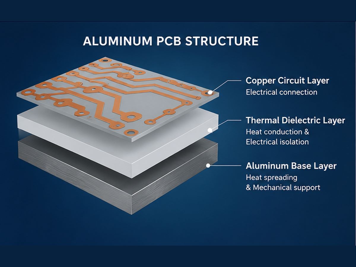
An aluminum PCB is a printed circuit board that uses an aluminum base to spread heat away from components. In a conventional single-sided construction, the main functional layers are:

Copper circuit → thermal dielectric → aluminum base

The copper carries current and forms the circuit pattern. The dielectric beneath it electrically isolates the circuit while conducting heat toward the aluminum substrate. The metal base then spreads that heat over a larger area and toward the housing or heat sink.

This structure is common in LED lighting, power converters, automotive electronics, motor drives, power modules, and other products with concentrated heat sources.

An aluminum PCB is one type of metal core PCB, or MCPCB. These terms are often used together in sourcing, but MCPCB is the broader category: the core or base can also be copper or another metal.

This distinction matters when talking to a metal core PCB manufacturer. A supplier that handles several metal-base structures may have more options when an aluminum substrate cannot meet the project’s thermal or electrical requirements.

aluminum PCB manufacturer

What Aluminum PCB Manufacturing Capabilities Should You Check?

A statement such as “we manufacture aluminum PCBs” tells you very little about whether a supplier can actually build your design.

The useful comparison starts with the parameters that affect the fabrication drawing and stackup:

  • Thermal material
  • Board structure
  • Copper thickness
  • Board thickness
  • Line width and spacing
  • PTH and NPTH capability
  • Board dimensions
  • Routing and slots
  • Outline tolerance
  • V-scoring
  • Surface finish
  • Assembly support

EBest Circuit supports the following aluminum and metal-core PCB manufacturing capabilities:

CapabilityEBest Circuit
Thermal conductivity1–3 W/m·K standard; up to 8 W/m·K
Board structureSingle-, double-sided; selected multilayer
Copper thicknessInner 0.5–3 oz; outer 1–3 oz
Board thickness0.8–3.0 mm standard
Max. size480 × 1180 mm
Min. PTH0.45 mm
Outline tolerance±0.15 mm
Surface finishHASL, OSP, ENIG, Ag, Sn, gold finger

Special materials, heavier copper, tighter tolerances, thicker substrates, and non-standard structures can be reviewed according to the stackup and fabrication drawing.

One parameter should never be judged in isolation. Copper thickness is a good example.

Outer CopperStandard Line / Space
1 oz0.20 / 0.20 mm
2 oz0.25 / 0.25 mm
4 oz0.50 / 0.50 mm

A manufacturer may advertise a very fine minimum trace width, but that figure often applies only to light copper. If your aluminum PCB carries higher current and requires heavier copper, the practical line/space capability changes.

That is why aluminum PCB manufacturing should be reviewed as a combination of material, copper, geometry, mechanical processing, and testing—not as a list of isolated maximum values.

aluminum PCB manufacturer

What Materials Should an Aluminum PCB Manufacturer Offer?

When comparing metal core PCB material, many buyers focus first on the aluminum sheet. In practice, the thermal dielectric deserves at least as much attention.

A conventional aluminum PCB stack contains three main materials:

  • Copper foil — carries current and forms the circuit.
  • Thermal dielectric — transfers heat while maintaining electrical isolation.
  • Aluminum substrate — spreads heat and provides mechanical support.

The dielectric sits directly in the thermal path. Its conductivity, thickness, dielectric strength, adhesion, and temperature behavior can therefore have a major effect on board performance.

This is also why the phrase “3 W/m·K aluminum PCB” does not describe the entire thermal design. Two materials with the same nominal conductivity can have different dielectric thicknesses, insulation characteristics, or thermal resistance.

For a power or thermal design, specify the material system around the actual requirement:

  • Thermal conductivity
  • Dielectric thickness
  • Dielectric strength
  • Copper weight
  • Finished board thickness
  • Operating voltage
  • Mechanical requirements

EBest Circuit’s standard material range includes 1, 2, and 3 W/m·K thermal material classes, while higher-conductivity options from 3 to 8 W/m·K can be evaluated when the application requires them.

Higher thermal conductivity is useful only when it solves an actual thermal bottleneck. A higher headline W/m·K value should not replace a proper review of the complete heat path.

How Do You Verify an Aluminum PCB Manufacturer’s Quality?

A good-looking aluminum circuit board can still have problems that are difficult to see from the surface. Dielectric integrity, copper geometry, hole dimensions, mechanical tolerances, and insulation all matter to finished-board reliability.

A supplier review should therefore cover three areas.

Material control

The factory should be able to identify and trace the aluminum laminate, dielectric system, copper foil, and other critical materials used for the order.

Material substitution matters more than it may appear. A different dielectric can change thermal conductivity, insulation performance, thickness, adhesion, or mechanical behavior even when two finished boards look nearly identical.

Fabrication control

Useful checkpoints for an aluminum PCB include:

  • Copper etching
  • Finished copper thickness
  • PTH and NPTH dimensions
  • Routing and slot dimensions
  • Board outline
  • V-score condition
  • Solder mask
  • Surface finish
  • Electrical continuity
  • Electrical isolation

Mechanical processing also deserves attention because the metal substrate behaves differently from standard FR4 during drilling, routing, and V-scoring.

Quality-system control

The required level depends on the end product. Automotive, industrial, medical, aerospace, and other reliability-sensitive projects may require additional traceability, inspection records, process controls, or specific quality-system certifications.

Certificates are useful, but they are not the entire qualification process. The PCB drawing, material specification, acceptance criteria, inspection plan, and test requirements should agree before production starts.

How Do You Choose the Right Aluminum PCB Manufacturer in China?

Start with the requirement that gives you the least design flexibility. That usually removes unsuitable suppliers faster than comparing website claims or company size.

ProjectCheck First
LED lightingThermal material
Power electronicsDielectric + copper
AutomotiveQuality + traceability
PrototypeEngineering response
Thick copperEtching capability
Complex outlineMechanical tolerance
OEM PCBAPCB + assembly
Volume productionRepeatability

For a standard one-layer aluminum PCB, an online manufacturer can be a very efficient option. If the board fits a published process window for material, thickness, copper, dimensions, and surface finish, there may be little reason to complicate sourcing.

The decision changes when the design includes heavier copper, a non-standard dielectric, unusual PTH or NPTH features, tight mechanical dimensions, multilayer construction, or customer-defined testing.

At that point, engineering communication becomes part of the manufacturing capability.

The same applies when the board will be assembled. Aluminum PCBs often carry LEDs, MOSFETs, power devices, drivers, converters, or other components that generate heat. PCB fabrication is only one part of the final thermal path.

If one supplier handles PCB fabrication and PCBA, the engineering review can also consider component placement, soldering, thermal interfaces, inspection, and functional testing.

For an OEM project, send the same controlled RFQ package to two or three shortlisted aluminum PCB manufacturers. Compare more than the quoted unit price.

Pay attention to the questions each supplier asks.

A manufacturer that checks the dielectric, copper weight, stackup, hole structure, outline, panelization, assembly requirements, and testing is showing you how it approaches manufacturability before the board reaches production.

What Should You Send for an Aluminum PCB Quote?

A Gerber file and quantity may be enough for a very simple board. For a customized aluminum PCB, they leave too much open to interpretation.

For bare-board fabrication, provide:

  • Gerber or ODB++ files
  • Fabrication drawing
  • Board dimensions
  • Layer structure
  • Thermal material requirement
  • Finished copper weight
  • Finished board thickness
  • Surface finish
  • PTH / NPTH requirements
  • Slots and routing details
  • V-score requirements
  • Quantity
  • Inspection or testing requirements

If thermal conductivity is specified, make it clear what the value refers to. The manufacturer should not have to guess whether the requirement applies to the dielectric, laminate system, or another thermal interface.

For PCB assembly, also provide:

  • BOM
  • Pick-and-Place / CPL file
  • Assembly drawing
  • Approved manufacturer list, if applicable
  • Programming files
  • Inspection requirements
  • Functional-test requirements

Complete RFQ data helps the manufacturer identify material or manufacturing conflicts before quotation instead of discovering them after production has already started.

FAQs About Aluminum PCB Manufacturers in China

Is an Aluminum PCB the Same as an MCPCB?

Not exactly. An aluminum PCB is one type of MCPCB. Metal core PCB is the broader term and can include aluminum, copper, or other metal-base structures. Aluminum is common because it offers a practical combination of thermal performance, weight, machinability, and cost.

Can Aluminum PCBs Be Multilayer?

Yes. Aluminum PCBs are not limited to simple one-layer LED boards. Several manufacturers offer double-sided or multilayer metal-base structures, although available stackups and fabrication limits vary considerably between suppliers.

What Thermal Conductivity Should I Choose for an Aluminum PCB?

Choose the dielectric according to the actual thermal and electrical requirements rather than automatically selecting the highest W/m·K rating. Dielectric thickness, insulation requirement, copper weight, component losses, board area, and the downstream heat sink all affect the final temperature.

Can an Aluminum PCB Manufacturer Also Provide PCB Assembly?

Yes. Many China-based aluminum PCB manufacturers also provide component sourcing, SMT/THT assembly, inspection, and testing. A combined service can reduce handoffs when the project moves from bare-board fabrication into PCBA production.

When Should I Consider Copper Core Instead of Aluminum?

Copper-base constructions become worth evaluating when heat flux, current density, or the required thermal path exceeds what a conventional aluminum structure can provide efficiently. Copper offers stronger bulk thermal performance, but it also increases material cost and weight, so the change should come from the design requirement rather than material preference.

Need an Aluminum PCB Manufacturer for Your Project? If your project is already moving from design into prototype or production, EBest Circuit can review the aluminum PCB stackup, thermal material, copper weight, mechanical requirements, and manufacturability before fabrication. For PCBA projects, you can also submit the BOM, Pick-and-Place file, assembly drawing, and testing requirements for a combined PCB + assembly review. Send your project files to sales@bestpcbs.com for engineering review and quotation.

You may also like

940nm Automotive IR LED Aluminum PCB for Camera Illumination

August 20th, 2026

A 940nm automotive IR LED aluminum PCB is used in automotive camera illumination systems such as driver monitoring and occupant monitoring, where 940nm IR LEDs provide low-visible-glow illumination for cameras operating in low-light conditions. Its performance depends on camera sensitivity, IR radiant output, pulsed current, thermal resistance, LED placement and optical uniformity, so these factors must be evaluated together during PCB design, assembly and validation.

Are you facing these problems in a 940nm automotive IR LED aluminum PCB project?

  • IR output does not match the camera: The selected 940nm LEDs appear powerful enough, but the camera image is still dark or inconsistent.
  • Temperature rises more than expected: Peak current is acceptable on paper, but repeated pulses create excessive temperature at the LED or PCB.
  • Prototype illumination cannot be repeated easily: LED position, orientation, soldering or component variation changes the illumination pattern between builds.

As a professional one-stop PCB and PCBA service provider, EBest Circuit supports automotive IR LED aluminum PCB fabrication, component sourcing, PCB assembly, prototyping and mass production. Our solutions include:

  • Match illumination to the actual camera: Review sensor response, optical transmission, FOV and emitter characteristics before defining the required IR output.
  • Verify the real pulse load: Peak current must be reviewed together with pulse width, duty cycle, repetition rate and operating temperature.
  • Control what affects production consistency: The released LED part number, footprint, orientation, placement and assembly requirements should remain controlled from prototype through production.

Developing a 940nm automotive IR LED aluminum PCB? Send the PCB files, BOM, IR LED part number and operating conditions to sales@bestpcbs.com for manufacturing review.

940nm automotive IR LED aluminum PCB, https://www.bestpcbs.com/blog/2026/08/940nm-automotive-ir-led-aluminum-pcb/

Why Is a 940nm Automotive IR LED Aluminum PCB Used for Camera Illumination?

A 940nm automotive IR LED aluminum PCB is used when a camera illumination module needs low-visible-glow IR output, pulsed LED operation, heat transfer and controlled emitter positioning. Current 940nm automotive IR LEDs are specifically offered for driver monitoring, occupant monitoring, interior monitoring, gesture sensing and child-presence detection.

  • Reduced visible red glow: 940nm produces substantially less visible red glow than 850nm, which is useful when illumination operates inside a dark vehicle cabin.
  • Low-light camera illumination: 940nm emitters provide near-infrared illumination for camera-based in-cabin sensing when available visible light is insufficient.
  • High-current pulse operation: Automotive IR emitters can be designed for short high-current pulses. The allowable current depends on pulse width, duty cycle and temperature rather than a single current rating.
  • Thermal management: Heat generated at the emitter must pass through the LED package, solder interface and PCB into the mechanical heat-spreading structure.
  • Controlled LED positioning: Automotive 940nm emitters are available with circular, rectangular and tilted radiation patterns, so component position and rotation directly affect the illuminated field.
940nm Automotive IR LED Aluminum PCB, https://www.bestpcbs.com/blog/2026/08/940nm-automotive-ir-led-aluminum-pcb/

How Do Camera Sensitivity and Optical Filters Affect 940nm IR LED Radiant Power?

The required 940nm radiant output depends on how much usable infrared energy reaches the image sensor after losses through the optical system.

  • Sensor sensitivity at 940nm: Higher NIR quantum efficiency increases the camera response for a given amount of incident 940nm energy. Sony’s IMX775 shows that automotive sensors can be specifically optimized for this wavelength.
  • Lens transmission: The lens must transmit sufficient energy around the selected NIR wavelength.
  • Optical filters: IR-pass, band-pass or other filters can attenuate part of the 940nm energy before it reaches the sensor.
  • Protective covers: Dark camera windows or trim materials can introduce additional NIR transmission loss.
  • Working distance: As the illuminated field expands, the same radiant output is distributed over a larger area.
  • Target reflectivity: Skin, fabric and other cabin surfaces do not return the same amount of NIR energy to the camera.
  • Exposure conditions: Camera exposure and synchronization with the LED pulse influence how much reflected IR is captured.
  • Beam pattern: Narrow, wide, rectangular and tilted emitters distribute the available radiant output differently.

Electrical wattage should not be used as an optical-output specification. The SFH 4728BS A01 T1 datasheet separately specifies parameters such as radiant intensity and optical characteristics under defined operating conditions.

How Do Peak Current, Pulse Width and Duty Cycle Define the Load on a 940nm IR LED Aluminum PCB?

Peak current defines only the highest instantaneous current. Pulse width, duty cycle, repetition rate and operating temperature determine how the LED and PCB experience that load over time.

  • Peak current: Maximum current carried during each IR pulse.
  • Pulse width: Duration of the high-current event.
  • Duty cycle: Percentage of time the LED remains energized.
  • Repetition frequency: How frequently the pulse repeats.
  • Forward voltage: Together with current, determines instantaneous electrical input.
  • Simultaneous LED count: Multiple emitters operating together increase total board and connector current.
  • Operating temperature: Permissible pulse current changes as component temperature rises.

The SFH 4728BS A01 T1 specifies 1.5A maximum forward current and up to 5A pulsed forward current only when tp ≤ 10ms and D ≤ 0.25. Its permitted operating current also varies with pulse and thermal conditions.

For a 940nm IR LED aluminum PCB, specify the complete pulse profile rather than only a maximum current value.

How Should Thermal Resistance Be Controlled in a Pulsed 940nm Automotive IR LED Aluminum PCB?

Thermal resistance must be controlled across the complete path from the LED junction to the housing. The aluminum base is only one part of that path.

For a conventional single-layer aluminum IMS, the thermal path is typically:

LED junction → package thermal pad → solder joint → copper circuit layer → thermally conductive dielectric → aluminum base → thermal interface/contact → housing or heat spreader

Insulated metal substrates are specifically used to reduce thermal impedance and conduct heat from high-watt-density surface-mount assemblies.

Control the thermal path by:

  • Maintaining the LED thermal pad area: Follow the released package footprint instead of reducing the heat-transfer area for routing convenience.
  • Controlling the solder interface: Poor wetting, insufficient solder or excessive voiding beneath the thermal pad can increase interface thermal resistance.
  • Maintaining the approved PCB construction: The dielectric lies directly in the heat path, so an unapproved change in construction can alter thermal performance.
  • Controlling PCB-to-housing contact: Poor flatness or incomplete mechanical contact adds another thermal interface.
  • Controlling TIM where used: Excessive thickness or trapped air can reduce effective heat transfer.
  • Testing with the actual pulse conditions: Thermal verification should reproduce the specified current, pulse width, duty cycle and ambient condition.

The SFH 4728BS A01 T1 specifies a maximum junction temperature of 145°C and a junction-to-solder-point thermal resistance of 3.9K/W typical and 4.7K/W maximum. These are component values, not the thermal resistance of the complete PCB and housing assembly.

How Should 940nm IR LED Placement and Beam Angle Match the Automotive Camera FOV?

LED placement should provide sufficient illumination across the camera’s horizontal and vertical FOV at the intended working distance.

  • Define the camera FOV: Use the actual horizontal and vertical field that requires illumination.
  • Define the working-distance range: Check coverage at relevant near and far positions.
  • Account for camera-to-LED offset: LEDs positioned beside the camera do not share the same optical axis.
  • Match beam pattern to the field: A rectangular camera field may be better matched by a rectangular IR emitter.
  • Control component orientation: Rectangular and tilted emitters require the correct PCB rotation.
  • Reference LEDs to mechanical datums: LED position should remain aligned with the camera and housing during final assembly.

Current automotive 940nm IR products include 60°, 80°, 150°, 110° × 135° and 130° × 155° beam patterns, together with tilted-emission variants.

The correct beam is the one that covers the required camera FOV with adequate irradiance, not simply the widest available emitter.

How Can a 940nm IR LED Array Reduce Hot Spots and Improve Illumination Uniformity?

Uniform illumination depends on LED spacing, beam overlap, emitter orientation and working distance.

  • Reduce center hot spots: Avoid concentrating the high-intensity centers of several beams in the same area.
  • Improve edge coverage: Review LED position and beam shape when the outer FOV receives insufficient illumination.
  • Prevent dark gaps: Adjacent emitters should provide adequate overlap at the intended working distance.
  • Use asymmetric beams where appropriate: Rectangular or tilted emitters can direct more energy toward areas that a circular beam covers inefficiently.
  • Control LED rotation: Orientation errors can shift rectangular or tilted patterns away from the required field.
  • Balance independent channels where available: Current adjustment can help correct some illumination imbalance, provided each emitter remains inside its specified limits.
  • Measure across the FOV: Optical validation should evaluate several positions across the camera field rather than only the optical center.

Automotive 940nm emitters with 110° × 135° and 130° × 155° rectangular patterns are already available for in-cabin sensing, showing that beam geometry is an application-level design parameter.

Adding more LEDs is not automatically an improvement; poor beam overlap can create stronger hot spots while also increasing current and heat.

What PCB Layout Details Matter for High-Current 940nm Automotive IR LED Arrays?

The PCB layout must carry the pulse current while preserving the LED thermal connection and optical position.

  • Current path: Route for the real peak current and simultaneous LED load, not only average current.
  • Compact pulse loop: Keep driver-to-LED and return paths short to reduce unnecessary resistance and parasitic inductance.
  • Branch consistency: Avoid unnecessary differences in path resistance between comparable LED branches.
  • Exact LED footprint: Use the released manufacturer’s land pattern.
  • Thermal pad connection: Preserve the intended thermal-contact area of the package.
  • Connector path: Include connector and cable resistance when the LED driver is located off-board.
  • Sensitive reference paths: Keep high di/dt LED current away from sensitive sensing or control references.
  • Optical orientation: Tie LED rotation to the camera or housing datum.
  • Temperature sensing: Position temperature sensors where they support the intended thermal-control or protection method.

The SFH 4728BS A01 T1 is supplied with package-specific dimensional and solder-pad requirements, reinforcing the need to design around the exact released emitter rather than a generic high-power LED footprint.

What Manufacturing and Assembly Controls Matter for a 940nm Automotive IR LED Aluminum PCB?

Manufacturing should reproduce the approved PCB construction, IR LED part number and optical geometry from prototype through production.

Step 1: Verify the released project files

Confirm the Gerber or ODB++, BOM, pick-and-place file, assembly drawing, exact IR LED ordering code, polarity, rotation and critical dimensions.

Step 2: Verify the LED footprint

Compare the land pattern with the current LED datasheet. For rectangular or tilted emitters, verify both electrical orientation and optical direction.

Step 3: Manufacture the approved PCB construction

Build according to the released copper, dielectric, aluminum base, surface finish, dimensions and mechanical tolerances. Review any proposed construction change before production.

Step 4: Control solder paste and placement

Control paste deposition, component centering and LED rotation because they affect solder quality, thermal contact and optical position.

Step 5: Follow LED handling and reflow requirements

The selected emitter’s current datasheet should control footprint, handling and reflow requirements. The cited SFH 4728BS family includes defined assembly requirements and package-specific solder information.

Step 6: Inspect the finished assembly

Check LED polarity, orientation, placement, solder condition and electrical operation. Perform thermal or optical verification when those acceptance limits are included in the project specification.

The SFH 4728BS A01 T1 also defines separate radiant-intensity groups, so the approved ordering code or permitted optical group should remain controlled when production uniformity depends on binning.

What Automotive Reliability Requirements Apply to a 940nm IR LED Camera Illumination Board?

Automotive reliability should be separated into component qualification and finished-module validation.

  • IR LED qualification: AEC-Q102 covers failure-mechanism-based stress-test qualification for discrete optoelectronic semiconductors used in automotive applications.
  • Component evidence: The current SFH 4728BS A01 T1 is identified by ams OSRAM as AEC-Q102 qualified.
  • Finished PCB validation: Qualification of the emitter does not qualify the assembled aluminum PCB.
  • Environmental requirements: The final camera illumination assembly may require temperature, cycling, vibration, power-cycling or other validation according to the vehicle program.
  • Traceability: PCB revision, BOM revision, IR LED ordering code and production-lot information should remain controlled when required by the project.

AEC-Q102-qualified LED ≠ AEC-Q102-qualified PCB assembly.

AEC-Q102 applies to the optoelectronic semiconductor component, not the complete 940nm automotive IR LED aluminum PCB.

How Should a 940nm Automotive IR LED Aluminum PCB Be Tested for Electrical, Thermal and Optical Performance?

A finished 940nm automotive IR LED aluminum PCB should be tested under actual or representative camera-module operating conditions.

  • Electrical performance: Check LED polarity, continuity, forward voltage, peak current, pulse width, duty cycle and repetition frequency. Measure the LED pulse waveform where the project requires waveform verification.
  • Thermal performance: Operate the board at the specified peak current, pulse width and duty cycle. Measure temperature at defined locations such as the LED solder area, aluminum base and housing interface. Compare the result with the selected emitter’s temperature limits.
  • Optical output: Where radiant output is specified, measure it using a defined current waveform, working distance and detector position.
  • Camera FOV coverage: Verify illumination across the required horizontal and vertical field, including the edges and corners.
  • Illumination uniformity: Measure IR intensity across multiple positions to identify center hot spots, dark edges and gaps between LED beams.
  • LED-to-LED consistency: For multi-LED arrays, check for abnormal differences caused by current variation, optical binning, component placement or assembly.
  • Board-to-board consistency: Compare representative production boards under the same drive and measurement conditions when optical consistency is part of the acceptance requirement.
  • Camera-level performance: When required, operate the board with the intended camera and verify the defined low-light image performance.
  • Test-condition control: Record ambient temperature, supply voltage, peak current, pulse width, duty cycle, working distance and camera or detector position so test results remain comparable.
  • Photobiological safety where applicable: If the finished IR source requires safety evaluation, IEC 62471 provides exposure limits, measurement methods and classification guidance for electrically powered incoherent optical sources, including LEDs, from 200nm to 3000nm.
940nm Automotive IR LED Aluminum PCB Testing, https://www.bestpcbs.com/blog/2026/08/940nm-automotive-ir-led-aluminum-pcb/

Why Choose EBest Circuit for 940nm Automotive IR LED Aluminum PCB Manufacturing?

For a 940nm automotive IR LED aluminum PCB project, the approved PCB, IR LED and assembly data need to remain consistent from prototype through production. EBest Circuit supports PCB fabrication, component sourcing and PCB assembly within its stated service scope.

  • Reduce coordination between PCB and assembly suppliers: PCB fabrication, component sourcing and PCB assembly can be handled within the same service scope, reducing unnecessary transfers of BOM, PCB revision and assembly information.
  • Keep the specified 940nm IR LED under BOM control: The customer-approved part number can remain tied to the released BOM rather than being treated as a generic 940nm emitter. This matters when beam pattern, package, optical-output group or pulse rating affects the finished module.
  • Carry prototype requirements into production: EBest Circuit supports PCB prototyping and mass production, allowing the approved PCB revision, footprint, orientation and assembly data to remain controlled as the project moves forward.
  • Support automotive manufacturing requirements: EBest Circuit’s supplied company information lists IATF 16949 and ISO 9001:2015 among its certifications.
  • Metal-based PCB manufacturing experience: Metal Core PCB is included in the company’s stated PCB product range, and EBest Circuit was founded in 2006.
  • Project-specific manufacturing review: Gerber or ODB++ files, LED footprint, BOM, placement data and pulse conditions can be reviewed against the released project requirements rather than replaced with generic aluminum PCB recommendations.
940nm Automotive IR LED Aluminum PCB, https://www.bestpcbs.com/blog/2026/08/940nm-automotive-ir-led-aluminum-pcb/

What Files and Specifications Are Required for a 940nm Automotive IR LED Aluminum PCB Quote?

For an initial 940nm automotive IR LED aluminum PCB quote, provide the PCB files, assembly data and actual IR LED operating conditions. Add thermal or optical acceptance requirements when they form part of the manufacturing scope.

PCB Fabrication Files

  • Gerber or ODB++ files
  • NC drill files
  • Fabrication drawing
  • Board dimensions and mechanical drawing
  • Approved PCB construction
  • Copper thickness
  • Surface finish
  • Critical dimensions and tolerances
  • Prototype or production quantity

PCB Assembly Files

  • BOM
  • Pick-and-place file
  • Assembly drawing
  • Exact 940nm IR LED manufacturer and part number
  • LED datasheet
  • Polarity and orientation requirements
  • Approved alternatives, if applicable

IR LED Operating Conditions

  • Supply voltage
  • Peak LED current
  • Pulse width
  • Duty cycle
  • Repetition frequency
  • Number of LEDs operating simultaneously
  • Driver or test-interface information where functional testing is required

Optical and Thermal Requirements

Provide these when applicable:

  • Camera FOV
  • LED beam pattern
  • Working distance
  • Required illumination area
  • LED position or rotation tolerance
  • Radiant-output requirement
  • Illumination-uniformity requirement
  • Thermal test conditions and temperature limits
  • Camera-level functional test criteria

If some specifications are still being finalized, the available Gerber or ODB++ files, BOM, LED part number and pulse conditions are sufficient to begin an initial manufacturing review.

FAQs About 940nm Automotive IR LED Aluminum PCBs

The question topics below were selected from recurring community discussions about 850nm versus 940nm camera compatibility, IR visibility, IR-cut filters, beam coverage and external IR illumination on Reddit and other electronics communities. The technical answers are based on device or standards information rather than community claims.

Q1: Can a camera that works with 850nm IR also work with a 940nm illuminator?

A1: Compatibility depends on the image sensor and complete optical path. A camera may detect both wavelengths but have substantially different sensitivity at each. Before moving from 850nm to 940nm, check the sensor spectral response and filter transmission. Sensors can also be optimized specifically for 940nm; Sony’s IMX775 specifies 35% QE at 940nm.

Q2: Why can the same 940nm illuminator look much brighter on one camera than another?

A2: The result depends on the sensor’s 940nm response, lens and filter transmission, exposure conditions and camera processing. The same IR source can therefore produce different image brightness on different cameras. Evaluate the LED with the intended production camera, not by LED wattage alone.

Q3: Is a 940nm IR LED completely invisible?

A3: It is safer to describe 940nm as having very low visible red glow rather than guaranteeing absolute invisibility. ams OSRAM describes 940nm as virtually invisible with only slight red glow, while community users also report that faint emission can still be noticeable under some dark-viewing conditions.

Q4: Does LED binning matter in a multi-LED 940nm array?

A4: Binning matters when the application requires controlled optical output between LEDs or production boards. The SFH 4728BS A01 T1, for example, is supplied with defined radiant-intensity groups. Control the approved ordering code or permitted bin range when optical consistency is part of the specification.

Q5: Can a narrower 940nm LED beam improve useful illumination distance?

A5: A narrower radiation pattern concentrates more of the available radiant output within a smaller angular field, while a wider pattern distributes it across a larger field. The correct choice should therefore balance irradiance and required camera FOV, not distance alone. Current automotive 940nm products range from relatively narrow patterns to 150° and rectangular 130° × 155° options.

Q6: Can a 940nm IR LED be driven far above its continuous-current rating if the duty cycle is low?

A6: Only within the pulse limits stated in the exact LED datasheet. Permitted peak current depends on pulse width, duty cycle and temperature, not duty cycle alone. The SFH 4728BS A01 T1 permits up to 5A pulsed current only under defined pulse conditions, while its continuous-current limit is lower.

Q7: Can an IR-cut filter prevent a camera from using 940nm illumination?

A7: A camera will receive less 940nm energy if its optical filter has low transmission at that wavelength, even when the image sensor itself has useful NIR sensitivity. This is why the sensor response and optical-filter transmission must be reviewed together before changing the IR wavelength.

Q8: Can one 940nm IR LED be replaced by another 940nm part without changing the PCB or optical design?

A8: The same nominal wavelength does not make two LEDs interchangeable. Parts can differ in package dimensions, solder pad, beam pattern, optical output, thermal resistance and pulse-current limits. ams OSRAM’s current 940nm automotive range alone includes 50°, 60°, 80°, 150°, rectangular and tilted-emission versions.

Q9: Should IR eye safety still be evaluated when 940nm light is difficult to see?

A9: Visible brightness is not a valid measure of infrared exposure. Where photobiological safety assessment is required, the complete source should be evaluated according to its radiant output, geometry and exposure conditions. IEC 62471 includes LEDs within its framework for incoherent optical-source safety.

Q10: What should be checked when prototypes work but production boards show different IR illumination?

A10: Compare the exact LED ordering code, permitted radiant-intensity group, drive waveform, LED rotation, XY placement, solder condition and camera alignment. Electrical continuity alone does not verify optical consistency. The SFH 4728BS A01 T1 datasheet itself defines different radiant-intensity groups, showing why component ordering information can matter in production.

A reliable 940nm automotive IR LED aluminum PCB must maintain the specified pulse current, heat path, emitter position and illumination geometry from prototype through production.

EBest Circuit provides metal-based PCB manufacturing, PCB prototyping, component sourcing, PCB assembly and mass-production services. Send your PCB files, BOM, IR LED data and operating requirements to sales@bestpcbs.com for manufacturing review and quotation.

You may also like

COB LED Aluminum PCB Manufacturing for High-Power LED Modules

August 19th, 2026

A COB LED aluminum PCB combines electrical routing with an efficient thermal path for high-power LED modules. Its performance depends on the dielectric layer, copper layout, LED interface and metal base working together. EBest Circuit supports metal core PCB projects from PCB design and prototyping to component sourcing, PCB assembly and mass production.

Are you worried about these COB LED aluminum PCB problems?

  • The COB LED still runs too hot after changing from FR4 to an aluminum PCB.
  • You are unsure which thermal conductivity, dielectric thickness or copper weight is actually needed.
  • The prototype works, but material or assembly consistency becomes difficult in production.

As a professional metal core PCB manufacturer, EBest Circuit can solve these issues by matching the PCB construction to the LED package, electrical load and thermal requirements. Below are our solutions:

  • Improve the Thermal Path
    Review the dielectric, copper spreading area and metal-base construction to reduce unnecessary thermal resistance.
  • Select the Right PCB Specifications
    Define thermal conductivity, dielectric thickness, copper weight and aluminum thickness from the actual LED power and current.
  • Keep Production Consistent
    Confirm the construction during prototyping and maintain the approved materials and assembly requirements in volume production.

Developing a high-power COB LED aluminum PCB? Send your PCB files, LED datasheet and project requirements to sales@bestpcbs.com for a quotation.

COB LED Aluminum PCB

What Is a COB LED Aluminum PCB and Why Is It Used for High-Power LEDs?

A COB LED aluminum PCB is a metal-based PCB designed to carry current and move heat away from a COB LED module. It is widely used in high-power lighting because the aluminum base can spread concentrated heat more effectively than a conventional FR4 structure.

A common single-layer construction is:

Copper circuit → thermal dielectric → aluminum base

In the finished LED module, heat typically travels through:

LED junction → LED package → solder or thermal interface → copper → dielectric → aluminum base → heat sink

The copper carries current and spreads heat around the LED area. The dielectric provides electrical isolation while transferring heat into the aluminum base, which distributes it across a larger surface.

The PCB should be designed around the actual COB LED package. Confirm the pad layout, thermal-contact area, optical center, package dimensions and mounting method from the LED datasheet before finalizing the footprint.

How Does a COB LED Aluminum PCB Improve Heat Dissipation?

A COB LED aluminum PCB spreads heat from the small COB LED area into a much larger metal surface. Heat moves through the copper and dielectric before reaching the aluminum base, so these intermediate layers directly affect thermal performance.

Three parameters matter most:

  • Dielectric Thermal Conductivity
    Higher conductivity improves heat transfer through the insulating layer. It should be evaluated together with dielectric thickness rather than used as a stand-alone specification.
  • Dielectric Thickness
    A thinner dielectric generally lowers thermal resistance, but it still needs enough dielectric strength and electrical isolation for the application.
  • Effective Heat-Transfer Area
    Adequate copper and thermal-contact area helps spread heat before it crosses the dielectric. This is especially important when a high-power COB concentrates heat into a small footprint.

Which Applications Use COB LED Aluminum PCBs and COB Light Engines?

COB LED aluminum boards are mainly used where high light output and concentrated heat occur in the same compact assembly.

Typical applications include:

  • Spotlights and Downlights: Compact products with limited space for the PCB and cooling structure.
  • Track and Architectural Lighting: Modules requiring stable output and accurate LED positioning.
  • High-Bay and Industrial Lighting: Higher-power products designed for long operating periods.
  • Streetlights and Floodlights: Outdoor lighting exposed to high power and elevated enclosure temperatures.
  • Stage Lighting: High-output sources operating at relatively high current.
  • Machine-Vision Lighting: Applications where stable illumination affects imaging and inspection quality.
  • Optical Inspection Equipment: Systems requiring precise LED positioning relative to optics.
  • Medical Illumination: Compact lighting modules requiring stable operation and repeatable assembly.
  • Projector and Imaging Light Sources: High-brightness systems with concentrated thermal loads.
  • COB Light Engines: Integrated modules combining the LED, PCB, optics and cooling structure.

For a COB LED module aluminum PCB, total LED power, operating time, ambient temperature and available cooling area matter more than the number of LEDs alone.

COB LED Aluminum PCB Application

How Should Thermal Conductivity, Dielectric Thickness and Copper Weight Be Selected?

For a COB LED aluminum PCB, these values should follow the LED power, operating current, thermal target and electrical-isolation requirement.

  • Select Thermal Conductivity From Heat Density
    Higher thermal conductivity is useful when the COB LED produces concentrated heat or when PCB area is limited. Moderate-power designs may not require the highest thermal class.
  • Keep the Dielectric Thin Without Sacrificing Isolation
    A thinner dielectric lowers thermal resistance, but it still needs to meet operating-voltage, dielectric-strength and manufacturing requirements.
  • Match Copper Weight to Current and Geometry
    Higher current may require heavier copper, but trace width and available copper area are equally important. Heavy copper does not correct an undersized current path.
  • Provide Enough Copper Around the Heat Source
    Larger copper areas around the COB LED improve lateral heat spreading before heat passes through the dielectric.
  • Avoid Increasing Specifications Without Finding the Limitation
    A higher W/m·K material or heavier copper provides little benefit if another part of the PCB construction limits thermal performance.
  • Validate the Construction During Prototyping
    Test the selected copper and dielectric construction at the intended LED power before freezing the design for production.

How Should the COB LED Footprint and Thermal Pad Match the Aluminum PCB?

Use the actual COB LED package drawing rather than a generic footprint. Similar-sized COB LEDs can have different electrical pads, thermal regions and mounting structures.

Check the following before release:

  • Electrical Pads: Match pad dimensions, spacing and polarity to the datasheet.
  • Thermal-Contact Area: Align the PCB thermal region with the package structure.
  • Optical Center: Position the emitting area correctly relative to the lens or reflector.
  • Solder Mask Clearance: Keep solderable areas fully exposed.
  • Package Outline: Leave enough clearance around the LED body.
  • Mounting Holes: Align the PCB with the LED module and heat sink.
  • Keep-Out Areas: Keep components and hardware away from optical or mounting areas.
  • Heat-Sink Interface: Maintain a flat and consistent backside contact area where required.

For soldered packages, solder volume also matters. Too much solder can increase stand-off or tilt the LED, while large voids under the thermal region reduce effective heat transfer.

Stencil openings, paste volume and reflow conditions should therefore be matched to the thermal-pad geometry.

When Should You Choose an Aluminum-Core PCB Instead of a Copper-Core PCB for COB LEDs?

Use an aluminum-core PCB when the required LED temperature can be achieved with the correct dielectric and cooling structure. Move to copper only when the thermal demand exceeds what an optimized aluminum MCPCB can support.

Choose an aluminum-core PCB when:

  • The Heat Density Is Within the Range of a Conventional MCPCB
    Aluminum works well for many spotlights, downlights, industrial lights, streetlights and other high-power LED modules.
  • The Dielectric Can Meet the Thermal Target
    If the correct dielectric conductivity and thickness provide enough thermal performance, a copper base adds limited value.
  • PCB Weight Matters
    Aluminum is lighter than copper and is suitable for larger lighting assemblies.
  • A Standard MCPCB Structure Is Preferred
    Aluminum-core PCB is widely used for both prototypes and volume LED production.
  • The External Cooling System Is Adequate
    If heat can move effectively from the PCB into the final cooling structure, aluminum is usually sufficient.

Consider a copper-core PCB when:

  • The COB LED Produces Very High Local Heat Flux
    A highly concentrated thermal load may benefit from stronger lateral heat spreading.
  • An Optimized Aluminum PCB Still Runs Too Hot
    Copper becomes more relevant after the dielectric and other major thermal limitations have already been addressed.
  • The Design Requires a Very Low-Resistance or Direct Thermal Path
    Some specialized LED constructions use copper-based structures to shorten the path between the heat source and metal substrate.
  • Thermal Performance Matters More Than Weight
    Copper provides higher bulk thermal conductivity but also increases PCB weight.

Use aluminum when it meets the thermal target. Move to copper only when the optimized aluminum structure is no longer sufficient.

What Steps Are Used to Manufacture and Assemble a High-Power COB LED Aluminum PCB?

A high-power COB LED aluminum PCB needs a controlled manufacturing process so the approved material, circuit and mechanical structure remain consistent through assembly.

Step 1: Review the Design and Material Requirements

Confirm the COB LED footprint, copper weight, dielectric, aluminum thickness, board dimensions, mounting holes, surface finish and required thermal interface.

Step 2: Prepare the Aluminum-Based Laminate

Use the approved copper, dielectric and aluminum construction. Material substitutions should be reviewed before production because they can change thermal and mechanical performance.

Step 3: Form and Etch the Copper Circuit

Image and etch the LED pads, power paths and supporting circuitry. Trace width and spacing must be compatible with the selected copper thickness.

Step 4: Drill and Profile the PCB

Produce mounting holes, slots and the finished outline according to the mechanical drawing. These features may align directly with the heat sink, lens holder or enclosure.

Step 5: Apply Solder Mask and Surface Finish

Keep COB LED pads and other solderable areas correctly exposed. The surface finish should match the intended assembly process.

Step 6: Print Solder Paste and Place Components

Control paste volume around the LED pads and place the COB LED accurately. Positioning may affect both electrical connection and optical alignment.

Step 7: Complete Reflow and Assembly Inspection

Use an appropriate reflow profile and check solder wetting, component orientation, stand-off and visible defects after soldering.

Step 8: Mount the PCB to the Cooling Structure

Install the assembled PCB using the specified TIM, screws or clamping arrangement. Avoid uneven contact or mechanical stress on the LED package.

Step 9: Verify Electrical and Thermal Performance

Operate the assembled module at the specified load and confirm current, LED function and operating temperature before volume production.

COB LED Aluminum PCB Manufacturing

What Steps Are Used to Inspect and Test a COB LED Aluminum PCB Before Shipment?

Inspection should cover the characteristics that can affect electrical operation, assembly fit and heat transfer.

Step 1: Verify Material and PCB Construction

Check the aluminum base, dielectric, copper thickness and finished PCB thickness against the approved specification.

Step 2: Check Dimensions and Mounting Features

Inspect the PCB outline, slots, mounting holes and critical dimensions to confirm fit with the mechanical assembly.

Step 3: Inspect Circuit and Surface Quality

Use visual inspection and AOI where applicable to identify opens, shorts, damaged pads, contamination, scratches or solder-mask registration defects.

Step 4: Perform Electrical and Insulation Testing

Verify circuit continuity and electrical isolation between the copper circuit and aluminum base.

Step 5: Check PCB Flatness

Inspect flatness when the PCB backside forms part of the thermal interface. Excessive warpage can reduce contact with the cooling surface.

Step 6: Inspect COB LED Placement and Soldering

Verify polarity, orientation, LED position, solder wetting and the condition of the main thermal-contact area.

Step 7: Perform Functional Testing

Operate the assembled module under the specified electrical conditions. Check for abnormal brightness, flicker, current behavior or other functional problems.

Step 8: Complete Thermal Validation

Test the module with the intended or representative cooling structure until temperature approaches a stable condition. Use thermocouples, thermal imaging or the LED manufacturer’s recommended method where appropriate.

Step 9: Confirm Production Consistency

Check that production boards use the approved materials, PCB construction and assembly requirements established during prototype validation.

COB LED Aluminum PCB Testing

What COB LED Aluminum PCB Manufacturing Capabilities Can We Provide?

Manufacturing capability determines whether the required COB LED aluminum PCB construction can be produced consistently from prototype to volume production. The table below summarizes our main MCPCB process capabilities for design and manufacturing reference.

ItemCapabilities
Maximum Layer CountUp to 10 layers
PCB Thickness0.3–4.0 mm
Maximum Board SizeUp to 610 × 1220 mm (24 × 48 in.)
Copper Weight0.5–10 oz
Minimum Trace / Space0.15 / 0.15 mm (6 / 6 mil)
Minimum Hole Diameter0.30 mm (12 mil)
Minimum Punch Hole Diameter3.0 mm (0.12 in.)
Minimum Hole Spacing0.40 mm (16 mil)
Maximum Aspect Ratio12:1
Minimum Solder Pad Diameter0.40 mm (16 mil)
Thermal Conductivity0.8–1.5 W/m·K standard; 2.0–6.0 W/m·K high thermal conductivity
Warp and Twist< 0.75%
FlammabilityUL 94V-0
Thermal Stress6 × 10 sec at 288°C
Surface FinishENIG, Flash Gold, Hard Gold, Selective Gold Plating, HASL, Lead-Free HASL, OSP, Immersion Silver, Immersion Tin

Case Study: High-Power COB LED Aluminum PCB From Prototype to Production

Project Background

A high-power COB LED module required an aluminum PCB connected to an external heat sink. The board had to provide a reliable thermal path while maintaining the correct LED position, mounting-hole alignment and mechanical fit.

Project Requirements

The PCB needed to:

  • Carry the required COB LED current
  • Transfer heat effectively to the cooling structure
  • Use an appropriate dielectric, copper weight and aluminum base
  • Match the LED footprint and thermal-contact area
  • Maintain PCB flatness and mounting accuracy
  • Support prototype assembly and later production

Our Solution

EBest Circuit reviewed the COB LED datasheet, PCB layout and mechanical drawing before prototype fabrication.

The main actions included:

  • Matching the COB LED footprint and thermal area to the package
  • Reviewing dielectric thickness, copper weight and aluminum construction
  • Providing sufficient copper around the main heat source
  • Controlling PCB flatness and mounting-hole alignment
  • Checking soldering, TIM contact and mechanical fit during prototype assembly
  • Maintaining the approved construction for production

Results

Prototype validation confirmed:

  • Stable COB LED mounting and alignment
  • Consistent PCB-to-heat-sink contact
  • A controlled thermal path
  • Reliable electrical and assembly performance
  • A repeatable construction for volume production

The approved PCB construction and assembly requirements were then carried forward into production.

What Specifications and Files Are Required for a COB LED Aluminum PCB Quote?

For a COB LED aluminum PCB quote, provide:

Bare PCB:

  • Gerber files
  • NC drill files
  • Board dimensions
  • Mechanical drawing
  • Finished PCB thickness
  • Copper weight
  • Aluminum thickness
  • Thermal conductivity requirement
  • Dielectric thickness or material requirement
  • Surface finish
  • Solder mask requirement
  • Quantity
  • Special tolerance or testing requirements

PCB Assembly:

  • BOM
  • Pick-and-place file
  • Assembly drawing
  • COB LED part number and datasheet
  • Polarity information
  • Functional-test requirements

For Thermal Review:

  • LED operating power and current
  • Heat-sink drawing
  • TIM specification
  • Mounting method
  • Expected ambient temperature
  • Maximum allowable operating temperature

If some specifications are still open, send the available project files first for review.

Why Choose EBest Circuit for COB LED Aluminum PCB Manufacturing?

With more than 20 years of PCB manufacturing experience, EBest Circuit supports COB LED aluminum PCB projects from prototypes through mass production.

  • One Supplier From Prototype to Production
    PCB prototyping, Metal Core PCB manufacturing, component sourcing and PCB assembly can be coordinated through EBest Circuit, reducing supplier handoffs.
  • Metal Core PCB Manufacturing
    Our PCB range includes Metal Core PCB / MCPCB, supporting COB LED modules and other thermal-management applications.
  • Capacity for Volume Production
    EBest Circuit has approximately 260,000 sq. ft. (28,900 m²) of monthly PCB manufacturing capability.
  • Support for Urgent Projects
    Expedited service is available for eligible projects, with qualifying urgent boards capable of shipment within 24 hours after requirements are confirmed.
  • Quality and Compliance
    EBest Circuit holds ISO 9001:2015, IATF 16949, ISO 13485:2016, AS9100D, UL, RoHS and REACH credentials.

Welcome to contact us if you have any request for COB LED aluminum PCB.

FAQs About COB LED Aluminum PCBs

Q1: Does a COB LED need a constant-current driver?
A1: Usually yes. A high-power COB LED is normally driven by a constant-current driver so current remains controlled as forward voltage changes. If the module already includes current regulation, follow its datasheet.

Q2: Should multiple COB LEDs be connected in series or parallel?
A2: Series connection is generally easier to control because each COB receives the same current. Parallel branches need current balancing because forward-voltage differences can produce unequal current sharing.

Q3: How should the LED driver voltage range match a COB LED?
A3: The driver’s output-voltage range must cover the forward voltage of the COB LED or complete LED string. Add the forward voltages of series-connected COB LEDs before selecting the driver.

Q4: Can a high-power COB LED be dimmed with PWM?
A4: Yes, when the driver supports it. Use the dimming method specified by the driver manufacturer rather than switching LED power directly.

Q5: Is it better to run a COB LED below its maximum rated current?
A5: Often yes. Lower current reduces thermal load and provides more operating margin. Select the working current from the LED manufacturer’s current, temperature and light-output data.

Q6: Can a COB LED be connected or disconnected while the driver is powered?
A6: It is better to avoid it. Hot-plugging can expose the COB LED to electrical transients. Turn the driver off unless the system is specifically designed for hot swapping.

Q7: Can a reflector or lens touch the COB LED?
A7: Optical parts should not press directly against the emitting surface or electrical contacts. Use a suitable holder to maintain alignment and prevent damage.

Q8: Can a failed COB LED be replaced on the MCPCB?
A8: In many designs, yes. Replaceability depends on the attachment method and thermal mass of the MCPCB. Rework temperature and heating time need careful control.

Q9: Should a high-power COB LED system include overtemperature protection?
A9: It is useful when cooling conditions can vary. Temperature sensing can reduce LED current or shut the system down if temperature exceeds the defined limit.

Q10: What happens if one parallel COB LED branch fails open?
A10: The remaining branches may carry more current when they share one constant-current source. Parallel designs should consider current balancing or independent current regulation.

Conclusion

A reliable COB LED aluminum PCB depends on the dielectric, copper layout, LED interface and metal substrate being matched to the actual electrical and thermal load.

EBest Circuit supports metal core PCB manufacturing, prototyping, component sourcing, PCB assembly and mass production. For a high-power COB LED aluminum PCB, COB LED module or light engine project, send your files and requirements to sales@bestpcbs.com for a quotation.
You may also like

Copper Direct-Thermal-Path MCPCB Design Guide for High-Power LEDs

August 15th, 2026

A copper direct-thermal-path MCPCB gives a high-power LED a shorter route from its thermal pad into the metal base. That reduction can preserve junction-temperature margin when a conventional insulated metal substrate becomes the dominant thermal bottleneck. The board is only one part of the system, however. Package compatibility, copper-pedestal geometry, solder quality, interface material, heatsink design, mounting pressure, ambient temperature, and airflow must all support the same thermal target.

This guide explains how to make that decision without relying on a universal wattage threshold. It also shows what to calculate, what to specify on the fabrication drawing, what to inspect during assembly, and how to validate the finished LED module before release.

Copper direct-thermal-path MCPCB for high-power LED thermal control

What Is a Copper Direct-Thermal-Path MCPCB and How Does It Work?

A Cu-DTP board places a controlled copper feature directly beneath the LED thermal pad, bypassing the dielectric in the primary heat path. In a conventional aluminum MCPCB, heat normally travels from the LED thermal pad through solder, copper foil, an electrically insulating dielectric, and then the aluminum base. The dielectric is thin, but its thermal conductivity is far below that of copper, so it may contribute a large share of the board-level thermal resistance.

In a direct-thermal-path construction, a copper pedestal or coin reaches the component-side thermal land. The LED thermal pad is soldered to this feature, allowing heat to enter the metal base without first crossing the dielectric. The surrounding signal and power pads remain on insulated circuitry. This structure improves the vertical heat route at the source while preserving electrical routing elsewhere on the board.

The word “direct” does not mean the complete module has zero thermal resistance. The remaining path still includes the LED package, solder joint, copper feature, baseplate, thermal interface material, heatsink, and convection or radiation to the environment. The practical benefit is the removal of one high-resistance layer from the most concentrated part of that path.

Heat-Path Element Conventional Aluminum MCPCB Cu-DTP MCPCB
LED thermal pad Soldered to surface copper Soldered to a controlled copper pedestal
Dielectric position Inside the primary vertical heat path Kept outside the direct pedestal path
Electrical isolation Provided continuously beneath the circuit layer Must be defined around the pedestal and routed pads
Main design benefit Simple, economical insulated-metal construction Lower source-to-base resistance at high heat flux
Main review risk Dielectric thermal resistance Pad compatibility, pedestal geometry, and process control

When Should You Choose a Copper Direct-Thermal-Path MCPCB Instead of an Aluminum MCPCB?

Choose Cu-DTP when the calculated junction-temperature margin cannot be met reliably after the conventional MCPCB dielectric and realistic interface losses are included. LED electrical input power alone is not a sufficient selection rule. Two modules operating at the same wattage may have very different heat flux, emitting area, ambient temperature, optical efficiency, enclosure geometry, and airflow.

Start with the complete thermal system. Treat the board, interface material, heatsink, enclosure, and airflow as one thermal system. A direct path is most valuable when the thermal source is concentrated, the package exposes a suitable thermal pad, the allowable temperature rise is small, and the heatsink can actually remove the heat delivered to it. If the external heatsink is already inadequate, lowering only the board resistance may move heat into a base that remains too hot.

  • Limited junction margin: The predicted maximum junction temperature is too close to the LED manufacturer’s limit after tolerances and worst-case ambient are included.
  • High local heat flux: A compact emitter or tightly spaced LED cluster concentrates heat into a small board area.
  • Dielectric-dominated loss: The standard MCPCB dielectric consumes an unacceptable share of the allowable board-to-heatsink resistance.
  • Optical stability requirement: The application needs tighter control of output, color, or electrical behavior over temperature.
  • Restricted cooling: A sealed enclosure, elevated ambient, limited airflow, or compact heatsink leaves little system-level margin.

A conventional aluminum MCPCB remains appropriate when its measured thermal performance meets the requirement with adequate production margin. Cu-DTP adds fabrication and assembly controls, so it should solve a quantified thermal problem rather than serve as a default material upgrade.

How Can You Confirm That an LED Package Is Compatible With a Direct Copper Thermal Path?

Compatibility depends first on the electrical function of the exposed thermal pad, not on LED power or package size. The copper pedestal may be electrically connected to the metal base or another defined potential. If the LED thermal pad is internally connected to an anode, cathode, or sensitive node, placing it on a shared conductive pedestal can create a short circuit or an unintended common connection.

Review the LED datasheet, package drawing, recommended land pattern, and electrical schematic together. Confirm whether the thermal pad is electrically neutral, internally connected, or required to remain isolated. For an array, check whether multiple emitters can share the same base potential. A package that works on one isolated pedestal may be unsuitable for several LEDs tied to a common copper base.

  1. Identify the pad: Match every bottom-side land in the package drawing to its electrical and thermal function.
  2. Confirm potential: Determine whether the exposed pad is floating, anode-connected, cathode-connected, or otherwise restricted.
  3. Check the circuit: Verify that the planned base and pedestal potential is compatible with series, parallel, or independently driven LEDs.
  4. Review isolation: Define the required spacing between the pedestal, routed copper, mounting hardware, and heatsink.
  5. Test continuity: Add an electrical isolation or continuity check that proves the manufactured board matches the intended connection scheme.

Do not approve the construction based only on a footprint library name. The exact ordering code and revision of the LED package must be part of the review because pad functions can differ within a product family.

How Do You Calculate the LED Junction-Temperature and Thermal-Resistance Budget?

Calculate the maximum allowable junction-to-ambient resistance from the worst-case temperature rise and the heat that must be dissipated. A useful first estimate is RθJA,max = (TJ,target – TA,max) / Pheat. Here, TJ,target is the selected design target rather than the absolute maximum rating, TA,max is the worst expected ambient temperature, and Pheat is the input power converted to heat.

Separate the available total resistance into the portions controlled by the package, board, interface, heatsink, and surrounding air:

RθJA = RθJ-PAD + RθPAD-BASE + RθTIM + RθHS-A

The labels must match the LED manufacturer’s defined measurement points. A published junction-to-case or junction-to-solder-point value is valid only when the temperature is measured at the specified reference location. Moving the thermocouple farther from the package can understate the estimated junction temperature because the measured board temperature is lower.

Budget Input Required Definition Common Error
Junction target Design value with reliability and performance margin Using the absolute maximum as the normal target
Maximum ambient Temperature at the module’s real installation location Using room temperature for an enclosed product
Heat dissipation Electrical input minus emitted optical power when reliable data is available Treating rated electrical power as a universal heat value without stating the assumption
Package resistance Datasheet value tied to the specified reference point Mixing junction-to-case and junction-to-solder-point definitions
Board and interfaces Worst-case manufactured and assembled values Using ideal material conductivity without contact resistance
Heatsink to ambient Characterized at the actual orientation and airflow Using a catalog value from different cooling conditions

A one-dimensional resistance network is useful for screening and budget allocation. It becomes less reliable for clustered LEDs, nonuniform boundaries, lateral spreading, several material regions, or heat leaving through multiple surfaces. Use a suitable thermal model and prototype measurements when geometry makes the simple network inconclusive.

Which Copper Direct-Thermal-Path MCPCB Specifications Affect Thermal Performance?

The specification must control the complete heat path, not merely call the board “Cu-DTP.” A fabrication drawing should identify the base material, base thickness, circuit copper, dielectric system outside the pedestal, pedestal material and dimensions, surface finish, isolation boundaries, outline, flatness, and the dimensions that require inspection.

  • Base material and thickness: Define the copper grade or approved equivalent and the finished base thickness that supports spreading, stiffness, and mounting.
  • Circuit copper: Specify finished copper thickness and current requirements for the LED power paths.
  • Dielectric system: Identify where insulation remains necessary and define its approved material rather than assuming it is irrelevant.
  • Pedestal geometry: Control the top size, height, location, and relationship to the finished board surfaces.
  • Surface finish: Select a solderable finish compatible with the LED termination, assembly process, storage period, and reflow profile.
  • Flatness and thickness: Set values that allow uniform TIM contact and predictable mounting pressure across the module.
  • Inspection features: Mark critical dimensions and electrical-isolation points so acceptance does not depend on a generic drawing note.

Material thermal conductivity is not a complete board specification. The effective resistance depends on the actual path length, area, interfaces, and manufactured geometry. Ask the supplier to confirm the proposed construction and controlled dimensions during DFM instead of relying on a trade name alone.

How Should the LED Thermal Pad and Copper Pedestal Be Designed?

The thermal land and copper pedestal must overlap consistently after fabrication and assembly tolerances are applied. The package land pattern defines solderable geometry, while the pedestal defines the direct heat-transfer area. If the two features are poorly registered, part of the thermal pad may sit over dielectric, solder mask, or a step in the surface.

Begin with the LED manufacturer’s recommended land pattern. Create a tolerance stack that includes package placement, copper imaging, pedestal machining or forming, layer registration, solder-mask registration, and any dimensional change during fabrication. The minimum guaranteed overlap—not the nominal CAD overlap—should carry the required heat flow.

LED thermal pad and copper pedestal alignment inspection for a Cu-DTP MCPCB

  • Thermal-land size: Follow package guidance unless a validated assembly study supports a controlled modification.
  • Solder-mask clearance: Prevent mask encroachment without creating an unnecessarily large exposed region.
  • Pedestal top area: Support the thermal pad while maintaining required clearance from electrical lands.
  • Surface coplanarity: Avoid a step that tilts the package or changes solder thickness across the terminations.
  • Paste definition: Use a stencil pattern that controls solder volume and gas escape for a large thermal land.
  • Inspection access: Plan X-ray, cross-section, continuity, or dimensional evidence for features that are hidden after assembly.

The design review should place the package drawing, paste layer, mask layer, copper land, pedestal boundary, and tolerance limits in one overlay. That comparison is more useful than reviewing each file separately.

How Is a Copper Direct-Thermal-Path MCPCB Manufactured and Controlled?

Manufacturing must form a repeatable direct copper feature while preserving insulation and coplanarity around the routed circuit. The exact sequence depends on the supplier’s qualified construction, but the control objectives remain the same: locate the pedestal accurately, bond or integrate the surrounding insulated circuit, finish the soldering surface, machine the outline, and verify electrical and dimensional acceptance.

  1. Review the construction: Confirm the pedestal concept, insulation boundary, material compatibility, and inspection plan before production data is released.
  2. Prepare the metal base: Form or machine the controlled copper feature using the supplier’s qualified method.
  3. Build the insulated circuit: Laminate or otherwise integrate the dielectric and circuit copper around the direct path without contaminating the pedestal surface.
  4. Image and etch circuitry: Create the LED power and signal features while maintaining clearance from the conductive base feature.
  5. Finish exposed lands: Apply the specified solderable finish with controlled coverage and thickness.
  6. Machine the board: Complete the outline, mounting holes, and thickness controls without distorting the contact surface.
  7. Inspect critical features: Measure pedestal position, top geometry, board thickness, flatness, surface condition, and electrical isolation.

A supplier may use different proprietary process details, so the buyer’s drawing should control measurable outputs rather than prescribe an unverified factory sequence. For initial qualification, request dimensional records and cross-sectional evidence for representative samples when the hidden structure is critical to acceptance.

How Do Soldering, TIM, Flatness, and Mounting Pressure Affect Heat Transfer?

A low-resistance board cannot compensate for a poor solder joint or an uneven board-to-heatsink interface. Solder voids reduce effective contact beneath the LED, while excessive solder can raise or tilt the package. At the opposite side of the board, a thick or incomplete TIM layer adds resistance and can prevent stable heat transfer into the heatsink.

Control solder paste volume, stencil aperture design, placement, reflow profile, and package coplanarity as one assembly system. Inspect the thermal joint using an appropriate method such as X-ray or cross-section during process qualification. Acceptance limits should reflect the location and continuity of voids, not only a total percentage that ignores whether a void interrupts the main heat route.

For the heatsink interface, use enough TIM to fill microscopic surface gaps without creating an unnecessarily thick bondline. Board and heatsink flatness determine how evenly that layer is compressed. Fastener placement and torque influence pressure distribution; excessive local force can bend the MCPCB, while insufficient force leaves high-resistance gaps. Electrically conductive TIMs also require clearance and contamination review.

Solder TIM flatness and mounting controls for copper direct-thermal-path MCPCB heat transfer

Interface Failure Mechanism Control or Evidence
LED-to-pedestal solder Voids, poor wetting, excessive thickness, or package tilt Stencil control, reflow record, X-ray, and section evidence
MCPCB-to-TIM Incomplete coverage or trapped debris Controlled dispense or pad placement and contact-imprint review
TIM bondline Excess thickness, pump-out, or dry regions Specified material, application amount, and cycling inspection
TIM-to-heatsink Roughness, contamination, or local air gaps Surface preparation and flatness verification
Mounting system Uneven pressure, board bending, or fastener relaxation Defined sequence, torque or force control, and post-cycle recheck

How Should a Finished High-Power LED Module Be Thermally Tested and Validated?

Validate the complete assembled module at worst-case power, ambient temperature, orientation, and realistic airflow. A bare-board material value cannot prove the operating junction temperature. The test must include the actual LED ordering code, solder process, MCPCB, TIM, heatsink, enclosure, mounting method, driver behavior, and cooling condition.

  1. Define the configuration: Record the LED code, current, electrical input, optical operating mode, board revision, TIM, heatsink, enclosure, orientation, and airflow.
  2. Select the temperature method: Use the LED manufacturer’s specified junction, case, or solder-point method and document the exact sensor location.
  3. Control the measurement: Minimize thermocouple heat sinking and attachment error; set emissivity deliberately when using thermography.
  4. Reach stabilization: Establish a criterion based on the rate of temperature change rather than an arbitrary short test time.
  5. Test operating limits: Repeat at maximum expected ambient, electrical tolerance, and realistic airflow restriction.
  6. Compare samples: Include enough assemblies to reveal variation in solder, flatness, TIM application, and mounting.
  7. Inspect after testing: Check solder alignment, joint condition, TIM coverage, fastener condition, board flatness, and electrical isolation.

Measure the temperature at the reference point defined for the LED’s published thermal resistance. A sensor placed farther away may report a lower temperature and make the calculated junction value appear safer than it is. For clustered LEDs, monitor the central and hottest devices rather than assuming every emitter operates at the average board temperature.

Thermal testing and validation of a high-power LED module on a Cu-DTP board

When technology selection remains uncertain, build controlled aluminum-MCPCB and Cu-DTP variants using the same LED, footprint, solder process, TIM, heatsink, mounting, power, ambient, and measurement method. The comparison then isolates the board construction more effectively than unrelated catalog values.

Which Thermal and Manufacturing Problems Commonly Affect Cu-DTP LED Boards?

Troubleshooting should separate local source defects, board-to-heatsink interface problems, and insufficient heat rejection to ambient. The temperature pattern across the LED, board, and heatsink usually indicates where to investigate first. Do not assume that every hot LED proves the MCPCB construction is defective.

Observed Symptom Probable Cause Discriminating Check
One LED is hotter than adjacent devices Local solder void, pad misalignment, LED variation, or current imbalance Compare current, X-ray evidence, placement, and the local temperature map
LED region is hot while the heatsink remains relatively cool Poor solder transfer, incomplete TIM coverage, excessive bondline, or weak mounting contact Measure both sides of each interface and inspect the TIM contact imprint
All LEDs and the heatsink base are hot Insufficient heatsink capacity, restricted airflow, or high ambient Repeat with characterized airflow or a known heatsink under the same electrical load
Temperature varies strongly among nominally identical boards Pedestal tolerance, board flatness, solder, TIM, or mounting variation Correlate thermal results with dimensional and assembly records
Temperature rises after repeated cycling TIM pump-out, fastener relaxation, joint degradation, or surface movement Recheck torque, bondline distribution, flatness, and thermal response after cycling
Electrical leakage or unexpected continuity appears Incorrect pad potential, inadequate clearance, conductive contamination, or isolation damage Perform continuity and insulation checks against the released connection scheme

Corrective action should follow evidence. For example, changing the heatsink will not repair pedestal misregistration, while tightening fasteners will not solve a solder void under one emitter. Retest the affected interface after each change and preserve the original operating conditions so the result remains comparable.

What Files and Specifications Are Required for a Copper Direct-Thermal-Path MCPCB Quote?

A useful quotation package must define the electrical design, direct-path geometry, mechanical interfaces, assembly state, and acceptance evidence. A board image or generic request for a “copper DTP PCB” does not give the supplier enough information to price tooling, tolerances, inspection, or assembly risk.

  • Fabrication data: Submit Gerber or ODB++ files, drill data, board outline, layer identification, and revision control.
  • Construction drawing: Define base material and thickness, circuit copper, dielectric regions, surface finish, pedestal geometry, flatness, and critical tolerances.
  • LED documentation: Include the exact ordering code, package drawing, recommended land pattern, datasheet, and exposed-pad electrical function.
  • Assembly files: Provide the BOM, centroid data, paste data, component orientation, stencil requirements, and approved reflow limits when assembly is requested.
  • Mechanical interface: Supply the heatsink drawing, mounting-hole details, TIM choice or target bondline, and fastening method.
  • Electrical requirements: State operating current, voltage, circuit topology, isolation requirement, and continuity test points.
  • Acceptance plan: Define dimensional inspection, cross-section or X-ray evidence, flatness, electrical test, sample quantity, and thermal validation responsibilities.
  • Commercial inputs: State prototype and production quantities, panel constraints if known, delivery location, and required documentation.

Ask the supplier to return a marked DFM review showing the proposed construction, exceptions, controlled dimensions, inspection method, and any assumptions used in the quotation. This turns the quote into a reviewable engineering proposal rather than a price based on an undefined trade name. For additional construction context, compare the proposed design with a dedicated direct thermal path copper PCB manufacturing process.
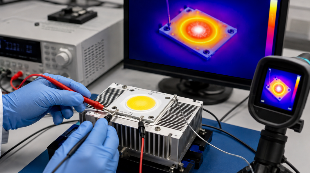
What Are the Most Common Questions About Copper Direct-Thermal-Path MCPCBs?

Q1: What does MCPCB stand for?

A1: MCPCB stands for metal-core printed circuit board. The metal base spreads heat, while the circuit layer routes power and signals to the LED.

Q2: Do high-power LEDs still need a heatsink with Cu-DTP?

A2: Yes, most high-power LED modules still need a suitable heatsink. Cu-DTP improves heat transfer into the base, but the module must still reject that heat to the environment.

Q3: What heatsink material works best with a Cu-DTP LED module?

A3: Select the heatsink by required thermal resistance, geometry, mass, airflow, weight, corrosion, and cost. Material conductivity alone does not determine the assembled result.

Q4: What are the best thermal interface materials?

A4: The best TIM is the one that meets the required interface resistance and assembly conditions at a controlled bondline. Compare electrical insulation, pump-out resistance, application method, service temperature, and rework needs.

Q5: What is thermal interface material made of?

A5: TIMs may use grease, phase-change compounds, filled elastomer pads, gels, adhesives, or other thermally conductive systems. The approved product must match the module’s electrical, mechanical, and reliability requirements.

Q6: Does copper have better thermal conductivity than aluminum?

A6: Bulk copper generally conducts heat better than bulk aluminum. That fact does not by itself prove that a finished copper board will outperform every aluminum MCPCB because dielectric and interface resistances also matter.

Q7: Why use aluminum instead of copper?

A7: Aluminum may be preferred when its thermal performance is sufficient and lower weight, material cost, or easier machining matters. Select the board from the complete thermal and mechanical requirement.

Q8: What is the maximum allowable LED junction temperature?

A8: Use the maximum junction temperature stated for the exact LED ordering code. Set the normal design target below that absolute limit to preserve margin for ambient, power, material, and assembly variation.

Q9: At what temperature should a high-power LED be soldered?

A9: Follow the LED manufacturer’s qualified reflow profile and exposure limits. Do not select a universal peak temperature without checking the package, solder alloy, board mass, and assembly process.

Q10: Why will solder not wet an LED MCPCB pad?

A10: Poor wetting commonly points to oxidation, contamination, insufficient flux activity, inadequate heating, or an unsuitable surface condition. Inspect the finish and process before increasing temperature or dwell time.

Conclusion

A successful Cu-DTP LED module begins with a thermal budget and ends with validation of the complete assembled heat path. Confirm the LED pad potential, define the copper pedestal and insulation boundaries, calculate realistic resistance allowances, control solder and heatsink interfaces, and test the module at its worst credible operating condition. The result should be judged by measured junction-temperature margin and repeatable manufacturing evidence—not by the board name alone.

If you need a DFM review or quotation for a copper direct-thermal-path MCPCB, email sales@bestpcbs.com with your Gerber or ODB++ data, fabrication drawing, LED datasheet, BOM, quantities, heatsink interface, operating conditions, and required inspection or thermal-test criteria.

You may also like

Copper Base PCB Thermal Solutions for Medical Diagnostic Devices

June 25th, 2026

A copper base PCB helps medical diagnostic devices control heat where standard FR-4 or aluminum PCB materials cannot provide enough thermal margin. It transfers heat from power components, optical modules, heater circuits and precision control areas into a copper base for faster heat spreading.

In diagnostic equipment, heat can affect test accuracy, signal stability, optical output, solder joint life and long-term reliability. Therefore, thermal design should not be treated as an afterthought. It should be reviewed together with the stack-up, dielectric layer, copper thickness, surface finish, assembly process and reliability test plan before production starts.

Copper Base PCB, https://www.bestpcbs.com/blog/2026/06/copper-base-pcb-2/

What Is a Copper Base PCB in Medical Diagnostic Devices?

A copper base PCB is a metal substrate PCB that uses copper as the main supporting and heat-spreading base. A typical structure includes a copper circuit layer, a thermally conductive dielectric layer and a copper base layer. The circuit layer carries electrical signals, while the copper base helps move heat away from high-power components.

In medical diagnostic devices, this structure is used when compact modules need both stable electrical function and strong heat dissipation. It is suitable for optical detection, thermal control, power conversion and high-current medical electronics where temperature drift may reduce device accuracy or service life.

Why Do Medical Diagnostic Devices Need Copper Base PCB?

Medical diagnostic devices need a copper base PCB when heat directly affects accuracy, reliability or operating stability. Many diagnostic systems combine sensors, LEDs, laser diodes, heaters, motors, power modules and analog circuits in a small enclosure. Without a stable thermal path, heat can spread into sensitive areas and disturb test results.

Key reasons include:

  • Improve temperature stability for optical, sensor and reagent control modules.
  • Reduce hot spots around LEDs, MOSFETs, drivers and heater circuits.
  • Extend component life by lowering repeated thermal stress.
  • Improve solder joint reliability during continuous operation and thermal cycling.
  • Support compact design where large heatsinks or fans are limited.

This makes copper substrate design valuable for high-reliability diagnostic equipment.

Which Medical Diagnostic Device Modules Use Copper Base PCB?

A copper base PCB is usually selected for modules that generate heat and need stable control at the same time. It is not required for every medical PCB, but it becomes important when temperature change may affect optical output, signal reading or power reliability.

Common application modules include:

  • PCR and qPCR thermal control modules
  • IVD analyzer heater boards
  • Fluorescence detection LED boards
  • Laser diode driver modules
  • TEC and Peltier control boards
  • Motor driver boards for pumps and scanners
  • Power supply and DC-DC converter boards
  • Imaging support power modules with localized high-power areas
  • Blood analyzer and biochemical analyzer heating or power control modules

These modules benefit from faster heat transfer and better temperature uniformity.

What Thermal Problems Can Copper Base PCB Solve in Diagnostic Equipment?

A copper base PCB can solve thermal problems caused by localized heat, poor heat spreading and unstable component temperature. In diagnostic equipment, these problems are not only electrical risks. They may also affect optical reading, reaction control and repeat test consistency.

Main problems include:

  • LED brightness drift caused by rising junction temperature.
  • Sensor signal offset caused by nearby power heat.
  • Reagent temperature instability in thermal control modules.
  • MOSFET overheating in motor, heater or TEC driver circuits.
  • PCB discoloration or solder fatigue after repeated operation.
  • Enclosure hot spots caused by poor heat transfer to the chassis.

The main value is stable heat movement from the component to the copper base and then to the final cooling path.

How Does Copper Base PCB Improve Heat Dissipation and Temperature Stability?

A copper base PCB improves heat dissipation by shortening the thermal path from the component to the heat-spreading base. Heat moves from the component pad to the copper circuit, passes through the thermally conductive dielectric layer and spreads across the copper base. This reduces local temperature concentration.

Copper has much better thermal conductivity than aluminum and FR-4, so it spreads heat faster across the board area. As a result, high-power components can operate at a lower and more stable temperature. For diagnostic equipment, this supports more stable optical output, lower power device stress and better long-term repeatability.

What Copper Base PCB Stack-Up Structures Are Used for Medical Diagnostic Devices?

Copper substrate stack-up should match power density, insulation needs, routing space and mechanical design. A simple single-sided structure may be enough for LED or heater modules, while double-sided or hybrid structures may be used when signal routing and thermal control must be combined.

TypeStructureUse Case
Single-sidedCircuit / dielectric / copper baseLED, heater, power module
Double-sidedCircuit / dielectric / copper core / dielectric / circuitMore routing and heat spreading
Thermoelectric separationDirect thermal pad and isolated circuitHigh-power LED, laser, TEC
Copper coinLocal copper insert under hot spotFocused heat removal
HybridFR-4 signal area plus copper thermal areaMixed signal and power design
Copper Base PCB Stack-Up, https://www.bestpcbs.com/blog/2026/06/copper-base-pcb-2/

How to Design the Thermal Path in Copper Base PCB?

Thermal path design should follow the real heat movement inside the device. The goal is to move heat from the component to the copper base, then to the chassis, heatsink, airflow or metal enclosure. A complete thermal path is more important than simply choosing a thick copper substrate.

Step 1: Confirm the main heat source
Identify LEDs, MOSFETs, TEC drivers, heater circuits, power ICs and motor drivers before layout. These parts should be treated as thermal design starting points, because their heat directly affects device stability.

Step 2: Place hot components near the heat-spreading area
Keep high-power components close to the copper base contact area, screw mounting area or chassis contact surface. Long heat travel paths increase thermal resistance and create local hot spots.

Step 3: Increase pad and copper contact area
Use larger thermal pads, wider copper areas and proper copper balance when the component package allows it. More contact area helps heat move into the board faster and reduces temperature concentration around one pad.

Step 4: Select the right dielectric layer
The dielectric layer must provide both insulation and heat transfer. A thinner or higher-conductivity dielectric can improve heat flow, but it must still meet voltage safety, reliability and medical device insulation requirements.

Step 5: Separate heat-sensitive circuits
Keep analog circuits, sensors and optical signal areas away from power heat sources. If the board space is limited, use spacing, copper isolation, grounding strategy and layout partitioning to reduce thermal interference.

Step 6: Design the final heat exit path
Heat should not stop inside the PCB. Plan how the copper base contacts the enclosure, heatsink, metal bracket or thermal interface material. Poor chassis contact can weaken the benefit of the copper structure.

Step 7: Verify the design by thermal simulation or prototype testing
Use thermal simulation, infrared thermal imaging or loaded prototype testing to confirm hot-spot position and temperature rise. If the heat map is uneven, adjust pad area, copper thickness, dielectric material or enclosure contact.

How to Choose Copper Thickness, Dielectric Layer and Copper Base Thickness?

Copper thickness, dielectric layer and copper base thickness should be selected according to current load, heat density, insulation voltage, mechanical strength and cost target. Thicker copper can improve current capacity and heat spreading, but it also increases etching difficulty, spacing limits and manufacturing cost.

ItemCommon RangeFocus
Circuit copper1 oz–10 ozCurrent and trace width
Dielectric thickness50 μm–150 μmThermal resistance and insulation
Dielectric conductivity1–12 W/mKHeat transfer and cost
Copper base0.5 mm–3.0 mm+Heat spreading and rigidity
Surface finishENIG, OSP, lead-free HASLSolderability and storage
Finished thicknessCustomEnclosure and assembly fit

The right choice is not always the thickest copper. It is the structure that meets the temperature target with stable yield and controlled cost.

Copper Base PCB vs Aluminum PCB: Which Is Better for Medical Diagnostic Devices?

A copper substrate is better for high-power, high-current and precision thermal control modules, while aluminum PCB is better for moderate heat and cost-sensitive designs. For medical diagnostic devices, the choice should depend on thermal margin, signal stability, working time, assembly structure and budget.

ItemCopper Base PCBAluminum PCBSelection Note
Thermal performanceHigher heat spreading capacityModerate heat spreading capacityChoose copper for high-density heat sources
Current capacityBetter for high-current pathsSuitable for medium currentCopper is better for heater, TEC and power boards
Temperature stabilityMore stable under heavy loadAcceptable for moderate loadCopper supports precision diagnostic modules
Mechanical strengthStrong and rigidGood, lighter than copperCopper works well for compact heavy-duty modules
WeightHeavierLighterAluminum is better when weight is critical
CostHigher material and process costLower total costAluminum is better for cost-sensitive projects
Processing difficultyHarder to drill, route and etchEasier to processCopper needs stronger process control
Fine line capabilityMore difficult with thick copperEasier in many common structuresReview DFM before using dense circuits
Heat source typeLocalized high-power componentsDistributed moderate heatCopper fits concentrated heat better
Medical application fitOptical, TEC, heater, power, motor driverGeneral thermal boards and low-risk modulesMatch material with risk level
Reliability marginHigher when designed correctlyGood for normal thermal loadCopper gives more margin for long operation
Typical limitationHigher cost and heavier weightLower thermal ceilingSelect based on performance target, not price alone

For optical detection, PCR heating, TEC control, laser diode driving and compact power modules, a copper substrate usually provides better safety margin. For simple control boards, low-power LED boards or moderate thermal loads, aluminum PCB may be enough and more economical.

What Design Factors Affect Copper Base PCB Reliability in Medical Equipment?

Reliability depends on how the copper base PCB handles heat, expansion, insulation, soldering and repeated operation. Medical diagnostic equipment often runs for long periods, so small thermal stress may gradually become solder cracks, dielectric damage or electrical instability.

Key reliability factors include:

  • CTE matching between copper base, dielectric, copper circuit and components.
  • Dielectric breakdown strength for insulation and safety margin.
  • Copper balance to reduce bow, twist and internal stress.
  • Solder joint design for heavy or high-temperature components.
  • Via reliability when plated holes or thermal vias are used.
  • Surface cleanliness to reduce leakage in sensitive circuits.
  • Surface finish stability for solderability and storage life.

A reliable design should pass both electrical and thermal verification.

What Manufacturing Challenges Affect Copper Base PCB Quality and Cost?

Copper substrate boards are harder to manufacture than standard FR-4 boards because copper is thick, heavy and difficult to process. Etching, drilling, routing, lamination, flatness control and surface finishing all affect quality and cost.

The manufacturing process begins with stack-up and DFM review. Then the copper base is prepared, cleaned and bonded with dielectric and circuit copper. After imaging and etching, the board goes through drilling, surface treatment, solder mask, routing, electrical testing, visual inspection and final packaging.

Common cost drivers include thick copper etching, high-conductivity dielectric, tight flatness control, copper base machining, ENIG finish, small-batch setup and medical traceability requirements. Early DFM review helps reduce redesign and production risk.

How to Test Copper Base PCB Reliability Before Medical Device Assembly?

Testing should confirm that the board can meet electrical, thermal, soldering and mechanical requirements before components are assembled. This is especially important for medical diagnostic devices because hidden thermal or insulation defects may affect long-term accuracy and reliability.

Step 1: Check the stack-up and material records
Confirm copper thickness, dielectric thickness, copper base thickness, surface finish and material batch records. This prevents wrong material selection before the board enters assembly.

Step 2: Run electrical testing
Use open, short, continuity and isolation testing to confirm that the circuit is electrically correct. This is the basic test before any thermal or assembly evaluation.

Step 3: Verify insulation performance
Use insulation resistance testing or hi-pot testing when the device has voltage isolation requirements. This helps detect dielectric weakness, contamination risk or insufficient insulation margin.

Step 4: Inspect appearance and dimensions
Check solder mask, pad shape, hole size, routing accuracy, bow, twist and surface scratches. Dimensional issues can cause poor assembly fit, unstable chassis contact or soldering problems.

Step 5: Use AOI and microscope inspection
Inspect line width, spacing, pad quality, solder mask registration and surface finish consistency. This is useful for dense diagnostic modules with small components or mixed power and signal areas.

Step 6: Perform microsection analysis when needed
Cross-section testing can check dielectric bonding, copper interface, plated hole quality and internal structure. It is useful when the board has thick copper, thermal vias or high-reliability requirements.

Step 7: Test solderability before SMT assembly
Solderability testing confirms that pads can wet properly during assembly. Poor solderability may cause weak joints, voids or unstable electrical contact after reflow.

Step 8: Use thermal imaging under load
Power the board under a controlled load and use infrared thermal imaging to locate hot spots. The test should confirm whether heat moves from the component area into the copper base as expected.

Step 9: Apply thermal cycling for reliability review
Thermal cycling helps evaluate repeated expansion and contraction stress. It is useful for heater circuits, TEC boards, optical modules and diagnostic equipment that runs for long periods.

Step 10: Review test data before assembly release
Compare all inspection results with the project requirement. Only boards with stable electrical results, acceptable thermal behavior and qualified solderability should move into medical device assembly.

Copper Base PCB Test, https://www.bestpcbs.com/blog/2026/06/copper-base-pcb-2/

Copper Base PCB Project Case for a Medical Diagnostic Device Thermal Solution

A medical diagnostic device customer needed a compact thermal solution for an optical detection module used in laboratory testing equipment. The first FR-4 prototype could pass short functional checks, but the LED excitation area became unstable during long operation. After repeated temperature cycles, the module showed brightness drift and inconsistent signal output

Project requirements:
The customer needed better heat dissipation without increasing the module size. The board also had to support stable LED output, reliable soldering, controlled insulation, repeatable assembly and smooth fitting with the metal enclosure. The design had to be suitable for prototype verification first, then small-batch production.

Our solution:
EBest Circuit reviewed the LED pad area, current path, dielectric layer, copper thickness, copper base thickness, solder mask opening and chassis contact position. The original FR-4 structure was changed to a copper substrate structure. We increased the thermal pad area, selected a higher thermal conductivity dielectric, optimized the heat path to the enclosure and added thermal imaging to the prototype test plan.

Output result:
The updated board reduced local hot spots and improved LED output stability during continuous operation. The customer received clearer stack-up data, better inspection criteria and a more reliable prototype for medical diagnostic device validation. After verification, the project moved into small-batch production with improved thermal consistency and lower assembly risk.

Copper Base PCB, https://www.bestpcbs.com/blog/2026/06/copper-base-pcb-2/

What Copper Base PCB Services Can EBest Circuit Provide for Medical Diagnostic Devices?

EBest Circuit provides custom copper base PCB fabrication and PCBA support for medical diagnostic devices. As a China source factory with global delivery capability, we help customers reduce thermal risk, shorten prototype validation time and improve batch production stability.

Our main services include:

  • PCB design review for copper thickness, dielectric layer, copper base thickness, insulation spacing and thermal path.
  • PCB prototype support for optical detection, heater, TEC control, power and high-current medical modules.
  • Mass production support with stable manufacturing capability for repeat orders.
  • Component sourcing to help overseas customers reduce BOM purchasing pressure.
  • PCB assembly support for medical diagnostic PCBA projects.
  • Thermal path optimization from components to copper base, chassis, heatsink or enclosure.
  • Quality inspection including electrical test, AOI, dimensional check, solderability review and thermal inspection.
  • Traceability control for material batch, production lot and inspection records.

Why Choose EBest Circuit as Copper Base PCB Manufacturer?

EBest Circuit was founded in 2006 and has over 20 years of PCB manufacturing experience. We provide one-stop support from PCB design, prototype and mass production to component sourcing and PCB assembly.

Customers choose us because we provide:

  • One-stop PCB and PCBA service
    Customers can manage design review, fabrication, sourcing, assembly and inspection through one supplier.
  • Lower prototype risk
    We review stack-up, copper thickness, dielectric layer, pad design and thermal path before production to reduce redesign and rework.
  • Better thermal reliability
    We support copper base PCB solutions for LED excitation, PCR heating, TEC control, heater circuits, motor drivers and power modules.
  • Stable production capability
    Our monthly production capability reaches about 260,000 square feet, supporting prototype, small batch and repeat production.
  • Quality system support
    EBest Circuit holds ISO 9001:2015, ISO 13485:2016, IATF 16949, AS9100D, UL, RoHS and REACH certifications.
  • China source factory advantage
    Customers can get custom manufacturing, flexible order support, global delivery and better cost control without unnecessary middleman layers.

For medical diagnostic device projects, EBest Circuit helps customers improve thermal stability, assembly yield, quality traceability and long-term supply reliability.

FAQs About Copper Base PCB for Medical Diagnostic Devices

Q1: When should a medical diagnostic device use a copper substrate instead of FR-4?
A1: A copper substrate should be considered when the module has high heat density, high current or strict temperature stability requirements. Common examples include LED excitation, TEC control, heater circuits and power modules. If FR-4 causes hot spots, signal drift or unstable output, a copper thermal structure can provide better reliability margin.

Q2: Is copper substrate necessary for every IVD analyzer board?
A2: No. Low-power control boards, communication boards and simple signal boards may still use FR-4. Copper substrate is mainly used in IVD modules where heat affects performance, such as heater boards, optical detection boards, motor drivers and compact power circuits. The material should be selected according to heat load and accuracy risk.

Q3: What affects the cost of a copper substrate PCB?
A3: Cost is affected by copper thickness, copper base thickness, dielectric thermal conductivity, board size, surface finish, routing difficulty, testing scope and order quantity. Thick copper, ENIG finish, tight flatness control and medical traceability can increase cost. Early DFM review helps control unnecessary process complexity.

Q4: Can copper substrate improve optical detection stability?
A4: Yes. Optical modules often use LEDs, laser diodes or excitation sources that are sensitive to temperature. Better heat spreading can reduce brightness drift, wavelength shift and local overheating. For fluorescence detection or optical sensing, stable temperature helps improve signal consistency during long operation.

Q5: What dielectric layer is suitable for medical diagnostic thermal boards?
A5: The dielectric layer should balance thermal conductivity and insulation strength. A high-conductivity dielectric improves heat transfer, while proper thickness maintains electrical safety. For medical diagnostic modules, selection should consider operating voltage, heat density, creepage, clearance and reliability testing, not only the thermal conductivity value.

Q6: Does thicker copper always mean better thermal performance?
A6: Not always. Thicker copper can improve current capacity and lateral heat spreading, but it also increases etching difficulty, spacing limits, weight and cost. The best design is based on actual current, temperature rise, component layout and production yield. Excessive copper thickness may create manufacturing risk without clear benefit.

Q7: Can copper substrate replace heatsinks or fans?
A7: It may reduce heatsink size or fan load in some compact modules, but it cannot replace the full cooling system in every case. Heat still needs to leave the PCB through the chassis, heatsink, airflow or enclosure. A complete system-level thermal path is required for stable long-term performance.

Q8: What tests should buyers request before medical device assembly?
A8: Buyers should consider electrical testing, insulation resistance testing, solderability testing, AOI, dimensional inspection, thermal imaging and microsection analysis when needed. For high-reliability modules, thermal cycling can also be added. The test plan should match the device risk level and working environment.

Q9: Can copper substrate boards support SMT assembly?
A9: Yes. Copper substrate boards can support SMT assembly, but the process should control solder paste volume, pad design, reflow profile, board flatness and component placement. Heavy copper and metal substrate structures may change heat absorption during reflow, so assembly parameters should be reviewed before batch production.

Q10: What files are needed for a copper substrate PCB quotation?
A10: Buyers should provide Gerber files, BOM, stack-up requirements, copper thickness, dielectric layer target, copper base thickness, surface finish, board quantity, assembly needs and test requirements. If the board is used in medical diagnostic equipment, traceability and inspection requirements should also be confirmed early.

Q11: How can buyers reduce risk before mass production?
A11: Start with prototype validation, then review thermal images, assembly yield, solder joint quality and electrical stability under load. Do not move directly to mass production before confirming the heat path and manufacturing tolerance. A small pilot run helps verify repeatability, test criteria and process stability.

Conclusion

A copper substrate board is a practical thermal solution for medical diagnostic devices when heat affects test accuracy, optical stability, current reliability or service life. The key selection point is not only the metal base material, but the full structure: copper thickness, dielectric layer, thermal path, enclosure contact, assembly process and reliability testing.

For procurement, buyers should confirm thermal targets, stack-up requirements, testing scope, traceability and assembly details before ordering. EBest Circuit provides custom copper substrate PCB fabrication and PCBA support from China for global medical diagnostic device projects. Send your Gerber files, BOM, stack-up target and thermal requirements to sales@bestpcbs.com for a project quotation.
You may also like

Aluminum vs Copper Heatsink: Which Is Better for PCB and PCBA Cooling?

June 23rd, 2026

When engineers compare an aluminum vs copper heatsink, they are usually looking for a better way to move heat away from electronic components. In PCB and PCBA projects, the heatsink is only one part of the thermal path. Heat must pass through solder joints, copper pads, PCB materials, thermal vias, metal cores, and finally to the heatsink, enclosure, or air. If this path is not well designed, even a high-performance heatsink may not fully solve overheating.

EBest Circuit (Best Technology) supports thermal management PCB and PCBA solutions, including aluminum PCB, copper core PCB, ceramic PCB, heavy copper PCB, and full turnkey PCB assembly. Since copper thermal conductivity is much higher than many common PCB materials, copper-based structures can help spread heat faster in high-power and high-current applications. Our engineering team can help review your PCB structure, copper thickness, material selection, component layout, and assembly requirements before production. If your project involves LED PCB, power electronics, automotive PCBA, industrial control boards, or high-current circuits, you can send your Gerber files, BOM, or thermal requirements to sales@bestpcbs.com for a practical engineering review.

Aluminum vs Copper Heatsink

Aluminum vs Copper Heatsink: What Is the Main Difference?

The main difference is simple: copper conducts heat better, while aluminum offers a better balance of weight, cost, and manufacturability.

Copper is useful when heat is concentrated in a small area. It can move heat away from power components faster, which helps reduce local hotspots.

Aluminum is lighter and easier to form into fins. Since heatsinks need surface area to release heat into air, aluminum is widely used for large cooling structures.

FactorCopperAluminum
Thermal conductivityHigherLower
WeightHeavyLight
CostHigherLower
Best useHotspots, compact high-power areasLarge fins, general cooling
PCB/PCBA roleHeat spreader, copper core, heavy copperAluminum PCB, MCPCB, external heatsink

In real products, many designs use both materials. A copper base spreads heat quickly, while aluminum fins provide larger cooling area with lower weight and cost.

Why Does Heatsink Material Matter in PCB and PCBA Thermal Design?

Heatsink material matters because it affects how quickly heat leaves critical components. But in PCB and PCBA design, it should not be selected alone.

A typical thermal path looks like this:

Component → solder joint → copper pad → PCB structure → heatsink → air or enclosure

If the PCB structure blocks heat transfer, the heatsink cannot work efficiently. For example, standard FR4 may not be enough for high-power LEDs, MOSFETs, IGBTs, or dense power modules.

Before choosing a heatsink, engineers should check:

  • Heat source position
  • Power density
  • Copper thickness
  • Thermal vias
  • Metal core material
  • Dielectric thermal conductivity
  • Component layout
  • Mounting pressure
  • Airflow and enclosure design

For low-power boards, FR4 with copper pours and thermal vias may be enough. For high-power products, aluminum PCB, copper core PCB, ceramic PCB, or heavy copper PCB may be more suitable.

Aluminum vs Copper Heatsink

Aluminum vs Copper Heatsink: Which Has Better Thermal Conductivity?

Copper has better thermal conductivity than aluminum.

Pure copper is usually around 385–401 W/m·K. Common aluminum materials are often around 205–237 W/m·K, depending on alloy grade and processing.

This means copper moves heat faster inside the material. When a component creates a small hotspot, copper can spread that heat more effectively.

However, heatsink performance also depends on surface area and airflow. Aluminum can be extruded into large fin structures, which helps release heat into the air at a lower cost and weight.

For PCB and PCBA cooling, the material choice often follows this logic:

NeedSuitable Option
Faster heat spreadingCopper core PCB, copper base, heavy copper
Lightweight coolingAluminum PCB, aluminum heatsink
High insulation and heat transferCeramic PCB
High current carryingHeavy copper PCB
General LED coolingAluminum PCB

Copper wins in conductivity. Aluminum often wins in cost, weight, and production practicality.

Why Are Most Heatsinks Made of Aluminum Instead of Copper?

Most heatsinks are made of aluminum because it is light, cost-effective, and easy to process.

Copper conducts heat better, but it is much heavier and more expensive. For the same size, copper is more than three times heavier than aluminum. In many PCBA products, that weight can create mechanical stress on the board or enclosure.

Aluminum can also be extruded into thin fins. This gives the heatsink more surface area, which is important for air cooling.

Aluminum is widely used in:

  • LED lighting modules
  • Power supply boards
  • Automotive electronics
  • Industrial control equipment
  • Communication devices
  • Consumer electronics
  • Aluminum PCB assemblies

Copper is usually used where its higher thermal conductivity brings clear value, such as copper bases, heat spreaders, copper cores, or high-power zones.

That is why aluminum is more common, but copper remains important in demanding thermal designs.

Do Copper Heatsinks Cool Faster Than Aluminum Heatsinks?

Copper can absorb and spread heat faster than aluminum. This is useful when heat is concentrated in a small area.

Typical examples include MOSFETs, IGBTs, power ICs, LED chips, processors, and high-current components. These parts can create local hotspots if heat is not moved away quickly.

But cooling speed is not decided by material alone. It also depends on:

  • Contact area
  • Thermal interface material
  • Mounting pressure
  • Fin design
  • Airflow
  • PCB copper area
  • Thermal via design
  • Soldering quality

A full copper heatsink may perform well, but it can be too heavy or expensive. In many cases, a copper base with aluminum fins is more practical.

At the PCB level, copper core PCB or heavy copper PCB can also help spread heat before it reaches the external heatsink. This can be more effective than simply adding a larger heatsink later.

Is Aluminum or Copper Better for PCB and PCBA Cooling?

For PCB and PCBA cooling, aluminum and copper solve different problems.

Aluminum is better when the product needs a lightweight, cost-controlled, and manufacturable cooling structure. It is widely used in LED PCB, power supply PCB, and many metal core PCB applications.

Copper is better when the design has high heat density, high current, or limited space. It is often used in copper core PCB, heavy copper PCB, copper inlay PCB, copper heat spreaders, or high-power thermal zones.

A practical selection rule is:

ApplicationCommon Thermal Choice
LED lightingAluminum PCB + aluminum heatsink
High-power LEDAluminum PCB, copper base, or ceramic PCB
Power supplyHeavy copper PCB + heatsink
Automotive power moduleCopper core PCB or ceramic PCB
Industrial control PCBAHeavy copper PCB or aluminum heatsink
High-current circuitHeavy copper, copper bus bar, copper core
Compact high-power moduleCopper spreader, ceramic PCB, copper core

The best material is not always the most expensive one. The right choice is the structure that keeps component temperature within a safe range while meeting cost, size, and reliability targets.

Aluminum vs Copper Heatsink

What Are the Weight and Cost Differences Between Aluminum and Copper Heatsinks?

Weight and cost are two major reasons aluminum is more common.

Copper has a density of about 8.96 g/cm³, while aluminum is about 2.70 g/cm³. For the same volume, copper is more than three times heavier.

This matters because many heatsinks are mounted directly on or near the PCBA. Extra weight can increase mechanical stress, screw requirements, vibration risk, shipping cost, and assembly difficulty.

Copper also costs more. It may require more careful machining and assembly control.

Aluminum is easier to process and better for large fin structures. It provides useful cooling area without making the product too heavy.

Still, the cheapest option is not always the best option. If poor thermal design causes overheating, unstable performance, LED lumen decay, or early failure, the total cost becomes much higher.

A cost-effective thermal design should match the PCB structure, heatsink material, and assembly process from the beginning.

When Should You Choose Copper-Based Thermal Solutions?

Choose copper-based thermal solutions when heat must move quickly from a small or high-power area.

Copper is suitable when the design has:

  • High heat density
  • High current
  • Limited board space
  • Compact structure
  • Strict temperature limits
  • Poor airflow
  • High reliability requirements

In PCB and PCBA manufacturing, copper-based solutions may include:

  • Copper core PCB
  • Heavy copper PCB
  • Copper inlay PCB
  • Copper coin PCB
  • Copper heat spreader
  • Copper base heatsink
  • Copper bus bar assembly

These options are common in power electronics, automotive modules, LED power boards, motor control, communication amplifiers, charging equipment, and other high-power products.

Copper should be used where its performance brings clear value. For many projects, copper near the heat source plus aluminum for larger dissipation area is a more balanced solution.

When Should You Choose Aluminum-Based Thermal Solutions?

Choose aluminum-based thermal solutions when the product needs good heat dissipation, lower weight, easier production, and better cost control.

Aluminum is suitable when the design has:

  • Moderate heat load
  • Larger cooling area
  • Cost-sensitive production
  • Weight-sensitive structure
  • LED lighting application
  • Good airflow or enclosure cooling
  • Mass production demand

In PCB and PCBA projects, aluminum is widely used in aluminum PCB, metal core PCB, LED PCB, power supply PCB, automotive lighting PCB, and industrial lighting modules.

Aluminum PCB is especially common in LED thermal management. It transfers heat from LED chips through the dielectric layer to the aluminum base, then to the heatsink or housing.

If the thermal requirement is not extreme, aluminum-based design is often the most practical choice. It offers a strong balance of performance, cost, weight, and manufacturability.

Why Choose EBest Circuit for PCB and PCBA Thermal Management Solutions?

Choosing between aluminum and copper heatsinks is only one part of thermal design. In many electronic products, the PCB and PCBA structure decide whether heat can move away from components efficiently.

EBest Circuit, also known as Best Technology, provides PCB and PCBA solutions for products that require stable heat dissipation. We support aluminum PCB, copper core PCB, ceramic PCB, heavy copper PCB, FR4 PCB, rigid-flex PCB, and turnkey PCB assembly.

We help customers select suitable thermal structures based on:

  • Power density
  • Current load
  • Heat source position
  • Product size
  • Working environment
  • Electrical insulation needs
  • Prototype or mass production quantity
  • Cost target

For LED lighting, automotive electronics, industrial control, power modules, communication equipment, medical electronics, and high-current PCBA projects, thermal performance is directly linked to reliability.

Our engineering team can help review Gerber files, stack-up, copper thickness, dielectric material, thermal vias, surface finish, BOM, component placement, and assembly requirements before production.

This helps identify thermal risks early, instead of discovering problems after PCBA testing or field use.

EBest Circuit supports both PCB fabrication and PCBA assembly, helping customers turn thermal design requirements into manufacturable products.

FAQs About Aluminum vs Copper Heatsink

1. Is copper better than aluminum for heatsinks?

Copper transfers heat faster, but aluminum is lighter, cheaper, and easier to form into large fin structures. Copper is better for high heat density. Aluminum is more practical for many general cooling designs.

2. Why are aluminum heatsinks more common than copper heatsinks?

Aluminum heatsinks are more common because they balance cooling performance, weight, cost, and manufacturability. Many products do not need full copper cooling.

3. Does copper dissipate heat better than aluminum?

Copper conducts heat better inside the material. But heat dissipation also depends on surface area, airflow, fin design, thermal interface material, and mounting quality.

4. Is a full copper heatsink worth it?

A full copper heatsink may be useful for compact, high-power products. For many designs, a copper base with aluminum fins gives a better balance.

5. Is aluminum or copper better for LED PCB cooling?

Aluminum PCB is commonly used for LED cooling because it is lightweight and cost-effective. Copper may be used for high-power LED modules that need faster heat spreading.

6. Is copper core PCB better than aluminum PCB?

Copper core PCB usually spreads heat better, but it costs more and is heavier. Aluminum PCB is suitable for many LED and power applications. Copper core PCB is better for higher heat density.

7. Can aluminum and copper be used together in one cooling design?

Yes. Many designs use copper near the heat source and aluminum for larger fin areas. This helps balance thermal performance, weight, and cost.

8. Can a heatsink solve all PCB overheating problems?

No. A heatsink works only when heat can reach it efficiently. If the PCB structure, solder pad, thermal vias, or dielectric material limit heat transfer, a larger heatsink may not fully solve the problem.

9. Which PCB material is best for thermal management?

There is no single best material for all products. Aluminum PCB suits many LED and power applications. Copper core PCB supports high heat density. Heavy copper PCB supports high current. Ceramic PCB is suitable for high thermal conductivity and insulation.

Choosing the right heatsink material is important, but reliable cooling depends on the full PCB and PCBA thermal path. If your project requires aluminum PCB, copper core PCB, ceramic PCB, heavy copper PCB, or turnkey PCBA with better heat dissipation, you can send your Gerber files, BOM, or thermal requirements to EBest Circuit at sales@bestpcbs.com for engineering review.

You may also like

Metal Backed PCB Supplier for Custom Thermal Management Solutions

June 23rd, 2026

A metal backed PCB is used when heat affects product stability, component life, and soldering reliability. In high-power electronics, poor heat dissipation can cause LED lumen decay, MOSFET overheating, solder fatigue, unstable output, and early failure.

Compared with FR4 PCB, a metal-backed PCB spreads heat faster through its metal base, making it suitable for LED lighting, power modules, motor drivers, charging systems, and industrial controls. This guide explains materials, design factors, heat transfer, cost, lead times, quality control, and EBest Circuit’s custom metal backed PCB manufacturing support.

Metal Backed PCB, https://www.bestpcbs.com/blog/2026/06/metal-backed-pcb/

What Is a Metal Backed PCB?

A metal-backed PCB, also called as IMS (Insulated Metal Substrate) or MCPCB (Metal Core PCB) , is a printed circuit board built with a metal base, a thermal dielectric layer, and a copper circuit layer. The metal base usually uses aluminum or copper, while the dielectric layer provides electrical insulation and transfers heat into the metal structure.

The main purpose is thermal management in high-power or high-temperature electronics. Compared with a standard FR4 PCB, this structure spreads heat faster and reduces local hot spots. It is also called MCPCB, metal core PCB, insulated metal substrate, aluminum PCB, or copper base PCB depending on the material and design.

What Problems Can Metal Backed PCBs Solve in High-Power Electronics?

Metal-backed PCBs solve heat-related problems that standard boards may not handle well. When power devices, LEDs, MOSFETs, drivers, or regulators generate heat in a small area, the board can suffer temperature rise, solder fatigue, material stress, and unstable electrical performance.

The key problems include:

  • Component overheating caused by poor heat spreading
  • LED lumen decay caused by high junction temperature
  • Solder joint cracks from repeated thermal cycling
  • Power derating when devices cannot operate at full load
  • Localized hot spots near high-current or high-power parts
  • Unstable performance inside compact enclosures with limited airflow

For projects involving metal backed PCB suppliers for power electronics, the supplier should review both electrical load and thermal load before confirming the stackup. This type of project needs heat flow analysis, insulation safety, soldering reliability, and production consistency.

How Does a Metal-Backed PCB Improve Heat Dissipation?

A metal-backed PCB improves heat dissipation by creating a shorter heat path from the component to the metal base. Heat first moves from LEDs, MOSFETs, drivers, or power chips into the copper circuit layer, instead of staying around the component pad.

Then, the heat passes through the thermal dielectric layer. This layer transfers heat downward while keeping the circuit insulated from the metal substrate. A lower thermal resistance dielectric helps heat move faster, but insulation safety must still be controlled.

After heat reaches the aluminum or copper base, the metal spreads it across a larger area. This helps reduce local hot spots, lower temperature rise, and improve long-term product stability.

The final result depends on dielectric thickness, thermal conductivity, copper area, component placement, and contact with the housing or heat sink. A good MCPCB design connects the heat source, thermal path, and external cooling structure together.

Metal Core PCB vs FR4 PCB: Which One Should You Choose?

Choose a metal backed PCB when heat dissipation, power density, and long-term thermal stability are the main design risks. Choose FR4 PCB when the product is low-power, cost-sensitive, or needs complex multilayer routing without heavy thermal load.

ItemMetal-Backed PCBFR4 PCB
Base MaterialAluminum, copper, or other metal substrateFiberglass epoxy laminate
Thermal PerformanceBetter heat spreading and lower hot spot riskLower heat transfer, relies on copper and airflow
CostHigher than standard FR4 PCBLower and widely available
Best UseLED, power electronics, motor drivers, chargersConsumer electronics, control boards, signal circuits
Mechanical StrengthBetter rigidity and heat sink contactFlexible for common PCB structures
Routing FlexibilityMore limited for complex multilayer designsBetter for dense multilayer routing
Assembly RiskRequires controlled soldering heat balanceEasier for standard SMT assembly
Design FocusThermal path, insulation, metal base contactSignal routing, layer count, component density

For high-power electronics, metal-backed PCB is usually the safer choice because the metal substrate moves heat away from power components faster than FR4 material. This helps reduce component overheating, LED lumen decay, solder fatigue, and thermal stress during long-term operation.

FR4 PCB is still the better option for many standard electronic products. If the board mainly carries control signals, low-current circuits, sensors, communication modules, or general SMT components, FR4 usually offers lower cost, easier fabrication, and better layout flexibility.

The final choice should be based on temperature rise, current load, component power, enclosure design, target cost, and assembly process. If heat is the main failure risk, choose a metal backed PCB. If routing complexity and cost are more important, FR4 PCB is usually more suitable.

metal core PCB vs FR4 PCB, https://www.bestpcbs.com/blog/2026/06/metal-backed-pcb/

Where Are Metal-Backed PCBs Commonly Used?

Metal-backed PCBs are used where heat, current, reliability, and compact space must be controlled together. These boards are common in products that run continuously or operate under high thermal load.

Common applications include:

  • LED lighting for street lights, high-bay lights, automotive lights, and UV LED modules
  • Power electronics such as converters, inverters, drivers, and power supplies
  • Automotive electronics including lighting, battery modules, sensors, and control units
  • Industrial equipment such as motor drives, automation controls, and power control boards
  • Telecom systems including RF modules, base station power boards, and thermal control boards
  • Charging products such as EV chargers, charging piles, and high-current power modules
  • Medical and commercial devices where stable operation and heat control affect reliability

In these applications, the PCB is not only used for electrical connection. It also supports heat transfer, mechanical mounting, and long-term product reliability.

What Materials Are Used for IMS PCB Manufacturing?

Metal backed PCB manufacturing mainly uses copper foil, thermal dielectric material, and a metal substrate. Aluminum is the most common metal base because it balances cost, weight, machinability, and heat spreading. Copper base is selected when the project has higher thermal load or higher power density.

MaterialFeatureCommon Use
Aluminum BaseBalanced cost and heat spreadingLED, power supply, control PCB
Copper BaseHigher thermal conductivityHigh-power module, compact power PCB
Steel BaseMechanical strengthSpecial structural PCB
Thermal DielectricInsulation and heat transferMetal core PCB structure
High-Tg LaminateBetter heat resistanceSoldering reliability and thermal cycling
Copper FoilCircuit and current pathPower traces and pads

Material selection should match thermal conductivity, insulation voltage, copper thickness, soldering temperature, mechanical strength, and operating environment. A low-cost material may pass a prototype but fail after long-term heat cycling, so material confirmation is an important early step.

What Design Factors Affect Metal-Backed PCB Thermal Performance?

Metal backed PCB thermal performance depends on the full heat path, not one material number. A high thermal conductivity value helps, but layout, copper distribution, dielectric thickness, component placement, and housing contact also decide the final temperature.

Key design factors include:

  • Dielectric thickness: thinner dielectric can reduce thermal resistance, but insulation must remain safe.
  • Thermal conductivity: higher conductivity helps heat move from copper to metal base faster.
  • Copper thickness: thicker copper improves current capacity and lateral heat spreading.
  • Component placement: high-power parts should connect to a short and direct heat path.
  • Pad and copper area: larger copper areas help distribute heat before it enters the dielectric layer.
  • Board flatness: better flatness improves contact with heat sinks or metal housings.
  • Surface finish: finish choice should support solderability, storage life, and assembly reliability.
  • Mechanical mounting: screws, thermal pads, and housing contact affect final heat transfer.

A good MCPCB design keeps the heat source, thermal path, and mechanical heat sink aligned. If these areas are separated, even a strong material may not deliver the expected thermal result.

How Do Integrated Thermal Vias Improve Metal-Backed PCB Heat Transfer?

Integrated thermal vias are most useful in metal backed PCB projects with double-sided structures, local heat transfer zones, or complex power layouts. They help connect hot copper areas to deeper copper layers, thermal pads, or special heat-spreading structures.

In some designs, thermal vias move heat away from power components before it concentrates around one local pad. However, the via design must consider hole filling, plating quality, insulation from the metal base, solder wicking, and assembly stability.

Experienced metal backed PCB suppliers should confirm whether integrated thermal vias truly improve the heat path before adding cost to the design. Poor via placement may increase cost without improving the actual thermal result.

What Special Requirements Matter for High-Tg Materials, Soldering Reliability, and Impedance Control?

Metal-backed PCB projects need extra control when the board works with high temperature, high current, thermal cycling, or mixed power-and-signal circuits. These factors affect material stability, solder joint strength, insulation safety, and signal performance.

  • High-Tg material:
    High-Tg material helps reduce warpage, delamination, softening, and dimensional change during lead-free soldering or long-term high-temperature operation. It is important for LED drivers, power modules, chargers, and industrial control boards.
  • Soldering reliability:
    A metal base absorbs and spreads heat faster than FR4 PCB, so soldering heat balance must be controlled. Pad size, copper area, stencil opening, surface finish, and reflow profile should be reviewed to reduce poor wetting, cold solder joints, voids, and solder fatigue.
  • Insulation safety:
    The dielectric layer must transfer heat and isolate the circuit from the metal base. For high-voltage or high-power products, insulation resistance and high-voltage testing help prevent leakage current, dielectric breakdown, and short risk.
  • Thermal cycling resistance:
    Copper, dielectric material, solder joints, and metal base expand at different rates. Poor material or layout control can cause pad lifting, solder cracks, dielectric separation, and stress around power components.
  • Impedance control:
    If the board includes control signals, RF areas, or communication lines, dielectric thickness, copper width, spacing, and stackup must be controlled. This helps reduce signal reflection, impedance drift, and unstable high-frequency performance.
  • Mechanical mounting:
    Screw holes, board flatness, housing contact, and heat sink pressure affect heat transfer. Poor contact can reduce thermal performance even when the material itself has good conductivity.

What Metal-Backed PCB Solutions Can EBest Circuit Provide?

EBest Circuit provides custom metal backed PCB manufacturing for projects that require thermal control, stable fabrication, assembly support, and file review before production.

  • Aluminum base PCB:
    Suitable for LED lighting, power supplies, control boards, automotive lighting, industrial electronics, and commercial thermal products. It offers balanced heat spreading, stable production, and controlled cost.
  • Copper base PCB:
    Suitable for compact high-power modules, power conversion products, and designs with higher heat density. It improves heat spreading but increases material cost, weight, and processing difficulty.
  • Single-sided MCPCB:
    Suitable for LED modules, power drivers, and simple thermal boards where components are placed on one side and heat transfers directly to the metal base.
  • Double-sided MCPCB:
    Used when the design needs more routing space, thermal vias, or special electrical connections. This structure requires tighter control of insulation, via quality, soldering balance, and flatness.
  • Custom material options:
    Copper thickness, dielectric material, board thickness, metal base type, and surface finish can be reviewed according to current load, heat path, insulation requirement, and cost target.
  • DFM review:
    Before production, EBest Circuit reviews Gerber files, drill files, stackup, copper distribution, hole design, insulation spacing, mounting holes, and panel design to reduce manufacturing risk.
  • PCBA support:
    For metal-backed PCBA projects, we can support PCB fabrication, component sourcing coordination, SMT assembly, soldering control, testing, inspection, and packing.

Metal-Backed PCB Project Case: Solving Overheating in a Power Electronics Module

Project background:
A compact power electronics module used an FR4 PCB. During continuous load testing, the MOSFET area became too hot, and the output became unstable after long operation. The enclosure space was limited, so the product structure could not be changed significantly.

Requirements and difficulties:

  • Move heat away from the MOSFET area faster without increasing board size.
  • Reduce local hot spots caused by poor FR4 heat spreading.
  • Keep the original enclosure and mounting structure as much as possible.
  • Improve solder joint reliability under repeated heating and cooling.
  • Prepare the design for repeat production, not only prototype testing.

Our solution:
EBest Circuit reviewed the Gerber files, copper layout, MOSFET placement, current path, screw hole position, housing contact area, and heat transfer route. The original copper area around the MOSFET pads was limited, so heat stayed near the power components.

We recommended a metal backed PCB with a shorter heat path from the MOSFET pads to the metal base. The copper area around the heat source was adjusted, the dielectric material was selected for both heat transfer and insulation, and the board structure was matched to the existing housing contact area.

We also reviewed pad connection, copper balance, and assembly heat absorption to reduce poor wetting, solder void risk, and thermal stress around high-power parts.

Output result:
After the pilot build, the heat path became clearer, housing contact improved, and the module ran more steadily during load testing. The project then moved into repeat production with inspection items for thermal structure, solderability, electrical function, insulation safety, and mechanical dimensions.

metal backed PCB, https://www.bestpcbs.com/blog/2026/06/metal-backed-pcb/

How Does EBest Circuit Evaluate Metal Backed PCB Quality Before Shipment?

EBest Circuit checks metal-backed boards before shipment through material confirmation, dimensional inspection, electrical testing, insulation review, visual inspection, and packing control.

  • Material check:
    Confirm metal base, dielectric layer, copper thickness, board thickness, and surface finish against the approved stackup.
  • Dimensional inspection:
    Check outline, holes, slots, thickness, mounting areas, and key tolerances to avoid assembly mismatch with housings, heat sinks, screws, or frames.
  • Electrical test:
    Use open and short testing to confirm circuit continuity before shipment.
  • Insulation test:
    Use insulation resistance or high-voltage testing when required to verify separation between the circuit layer and metal base.
  • Thermal path review:
    Check copper area, dielectric condition, exposed thermal zones, mounting surface, and metal base contact area to avoid blocked or weak heat paths.
  • Solder mask and finish check:
    Inspect solder mask coverage, pad exposure, surface finish, oxidation, stains, scratches, and contamination that may affect solderability.
  • Hole and routing check:
    Review vias, plated holes, non-plated holes, slots, routed edges, burrs, and hole position accuracy.
  • Flatness and appearance check:
    Check warpage, dents, scratches, wrong marking, exposed metal damage, and surface defects before packing.
  • Packing check:
    Pack boards with separation, labels, moisture protection when needed, and transport protection to reduce damage during international shipment.

What Affects Metal Backed PCB Cost and Lead Times?

Metal backed PCB cost and lead times mainly depend on material, structure, copper thickness, dielectric performance, tolerance, surface finish, testing, quantity, and file completeness.

  • Metal base material:
    Aluminum base is usually more economical and faster to arrange. Copper base improves heat spreading but increases cost, weight, machining difficulty, and lead time.
  • Thermal dielectric:
    Higher thermal conductivity or higher insulation voltage can improve performance, but special dielectric materials may cost more and require longer preparation.
  • Copper thickness:
    Thicker copper improves current capacity and heat spreading, but it increases etching difficulty, line control requirements, and production cost.
  • Board structure:
    Single-sided boards are faster and more cost-effective. Double-sided MCPCB, plated holes, thermal vias, or special structures add process steps and inspection time.
  • Mechanical complexity:
    Special outlines, slots, countersunk holes, dense mounting holes, strict flatness, and tight tolerances increase routing and inspection workload.
  • Surface finish:
    HASL, lead-free HASL, OSP, and ENIG have different cost and processing requirements. ENIG offers better flatness and storage stability but usually costs more.
  • Testing requirements:
    Electrical testing is standard. Insulation testing, solderability checks, dimensional reports, or special reliability tests add cost and time.
  • Order quantity:
    Prototype orders have higher unit cost because setup and process review are spread across fewer boards. Batch production can lower unit cost after process stability is confirmed.
  • File completeness:
    Complete Gerber files, drill files, stackup, material requirements, copper thickness, surface finish, tolerance, quantity, and test requirements shorten quotation and production review.
  • Material availability:
    Standard aluminum base materials are easier to schedule. Copper base, uncommon thickness, high thermal conductivity dielectric, or special surface finish may extend lead time.

Why Choose EBest Circuit as Your Metal Backed PCB Supplier?

Choose EBest Circuit when your project needs stable quality, custom support, fast response, and one-stop PCB and PCBA service. With over 20 years of PCB manufacturing experience, EBest Circuit helps reduce design risk, production delay, quality problems, and supplier communication cost. Here are reasons why choose EBest as your metal backed PCB supplier:

  • One-stop service:
    We support PCB design, prototype, mass production, component sourcing, and PCB assembly. This helps simplify the process from bare board fabrication to finished PCBA delivery.
  • Custom thermal solutions:
    We can review metal base material, dielectric layer, copper thickness, surface finish, insulation safety, and heat path design to match the product’s thermal requirements.
  • Prototype and batch production support:
    Prototype builds help verify thermal performance, soldering reliability, and mechanical fit before mass production. Batch production can follow with clearer quality standards.
  • Certified quality control:
    EBest Circuit supports projects with ISO 9001, IATF 16949, ISO 13485, AS9100D, UL, RoHS, REACH, and other quality and compliance requirements.
  • Flexible production capacity:
    With monthly capacity of about 260,000 square feet, EBest Circuit can support small trial orders, repeat production, and custom PCB projects.
  • Fast delivery for urgent projects:
    Expedited service is available for urgent boards, and some urgent PCB orders can be shipped within 24 hours when materials and files are ready.
  • Wide PCB technology coverage:
    We support metal core PCB, FR4 PCB, multilayer PCB, ceramic PCB, flexible PCB, rigid-flex PCB, RF PCB, high-Tg PCB, heavy copper PCB, HDI PCB, high-speed PCB, and impedance control PCB.

A reliable metal backed PCB supplier should help control thermal performance, insulation safety, soldering reliability, production quality, delivery schedule, and final assembly risk. EBest Circuit supports these needs from file review to shipment.

Metal Backed PCB, https://www.bestpcbs.com/blog/2026/06/metal-backed-pcb/

FAQs About Metal Backed PCB

Q1: Can metal-backed PCBs be used in outdoor products?
A1: Yes, they can be used in outdoor lighting, charging equipment, industrial controls, and power modules. The board should match the working environment, including humidity, temperature change, UV exposure, vibration, and enclosure sealing. For outdoor use, surface finish, solder mask, coating, connector protection, and housing contact should be reviewed before production.

Q2: Does solder mask color affect thermal performance?
A2: Solder mask color has limited influence compared with dielectric material, copper area, and metal base contact. However, color can affect visual inspection, marking clarity, and product appearance. For LED lighting, white solder mask is often used for better light reflection, while black, green, or blue solder mask may be selected for product design or assembly needs.

Q3: Can components be assembled directly on a metal-backed PCB?
A3: Yes. SMT components, LEDs, power devices, connectors, and some through-hole parts can be assembled on metal-backed boards. The assembly process should control thermal mass, reflow profile, pad wetting, and fixture support, because the metal base absorbs heat differently from standard FR4 PCB during soldering.

Q4: Are metal-backed PCBs suitable for high-voltage applications?
A4: They can be used in high-voltage products if insulation design is properly controlled. The key is to confirm dielectric strength, clearance, creepage, hole spacing, and test voltage before manufacturing. For high-voltage LED drivers, chargers, and power modules, insulation testing between the circuit and metal base is especially important.

Q5: Can a metal-backed PCB be connected to a heat sink?
A5: Yes. In many products, the metal base is mounted directly to a heat sink, metal housing, or chassis. To improve contact, the design may use screws, thermal pads, thermal grease, flat mounting areas, or controlled pressure. Poor contact can reduce thermal transfer even when the PCB material has good heat conductivity.

Q6: Can metal backed PCBs be cut into special shapes?
A6: Yes, metal-backed boards can be routed, milled, drilled, slotted, or made with special outlines. However, complex shapes increase machining difficulty. Sharp corners, narrow bridges, dense holes, and tight edge tolerances should be reviewed because they may affect routing quality, burr control, flatness, and mechanical strength.

Q7: Do metal-backed PCBs need conformal coating?
A7: Conformal coating is optional and depends on the product environment. It may be useful for products exposed to humidity, dust, salt mist, chemical vapor, or outdoor conditions. Coating should not block thermal contact areas, connector contact points, screw grounding areas, or heat sink mounting surfaces unless the design specifically requires it.

Q8: Can metal-backed PCBs support through-hole components?
A8: Yes, but through-hole design needs extra review. Since the metal base is conductive, hole insulation, spacing, plating structure, and assembly clearance must be controlled. For some structures, non-plated holes or insulated holes may be required to prevent short risk, soldering difficulty, or mechanical interference.

Q9: What information helps verify thermal performance before production?
A9: Useful information includes power device locations, estimated power loss, target operating temperature, housing material, heat sink structure, airflow condition, mounting method, and test environment. These details help confirm whether the selected board structure can support real heat transfer, not only theoretical material data.

Q10: Can metal core PCBs be used with adhesive thermal pads?
A10: Yes, thermal pads are often used between the board and housing or heat sink. The pad should match thermal conductivity, thickness, compression force, insulation requirement, and operating temperature. A pad that is too thick or poorly compressed can increase thermal resistance and reduce heat transfer.

Q11: What packaging is suitable for metal-backed PCB shipment?
A11: Packaging should protect the board from scratches, oxidation, moisture, bending, and edge damage. Metal-backed boards are usually packed with separation layers, vacuum or moisture-proof bags when needed, labels, and strong outer cartons. For international shipment, edge protection and surface protection are important.

Q12: Can EBest Circuit support both bare metal-backed PCB and assembled PCBA?
A12: Yes. EBest Circuit supports PCB design, prototype, mass production, component sourcing, PCB assembly, inspection, and shipment. This helps reduce handover issues between fabrication and assembly, especially for products that need thermal control, soldering reliability, component matching, and final PCBA testing.

Conclusion

A metal backed PCB is a practical solution for products where heat affects stability, component life, soldering reliability, and long-term performance. The right board should match the actual power load, heat path, insulation requirement, material structure, assembly process, and final enclosure design.

For custom projects, the safest approach is to review the files before production and confirm the metal base, dielectric layer, copper thickness, surface finish, mounting method, and testing requirements. This helps avoid overheating, weak insulation, poor soldering, delayed delivery, and unnecessary cost changes.

EBest Circuit provides custom metal backed PCB and PCBA manufacturing for global projects, including file review, prototype, mass production, component sourcing, assembly support, quality inspection, and shipment. Send your Gerber files, stackup, quantity, material requirements, and project details to sales@bestpcbs.com for a custom quote.

You may also like

LED Module Assembly: Building Reliable Lighting Boards

June 22nd, 2026

LED module assembly is not just about placing LEDs onto a PCB. A reliable lighting board needs the right PCB base, stable solder joints, correct LED polarity, controlled heat transfer, and suitable protection for the working environment.

For many lighting products, the customer already controls the final lamp housing, optics, driver, structure, and product-level validation. The PCB and PCBA partner focuses on the assembled lighting board: MCPCB fabrication, SMT LED mounting, soldering control, coating support, and basic testing.

This guide explains what buyers should know before sourcing LED module assembly for lighting boards.

LED Module Assembly

What Is LED Module Assembly?

LED module assembly is the process of turning a bare LED PCB into an assembled lighting board. It usually includes PCB fabrication, solder paste printing, SMT LED mounting, lead-free reflow soldering, inspection, testing, and sometimes protective coating.

In PCB manufacturing, an LED module does not always mean a complete finished lamp. It usually means the LED board inside the product. The housing, lens, driver, thermal structure, final packaging, and product certification may still belong to the customer’s final product scope.

This distinction matters. If you need only the bare board, you are requesting LED PCB or MCPCB fabrication. If you need LEDs mounted and tested, you are requesting LED module assembly or LED PCB assembly.

ItemLED PCBLED Module
StatusBare boardAssembled lighting board
LEDsNot mountedMounted and soldered
FunctionCannot light up aloneCan be powered and tested
Main servicePCB fabricationPCB + SMT assembly
Quality focusMaterial, copper, finishSoldering, polarity, function
LED Module Assembly

Why Are MCPCBs Used in LED Lighting Boards?

LEDs generate heat during operation. If heat stays near the LED package and solder joint, the module may face faster brightness decay, color shift, solder stress, or early failure. That is why many LED lighting boards use MCPCBs, especially aluminium core PCBs.

A metal-core PCB gives heat a better path from the LED pad area toward the metal base. This is especially useful for compact lighting boards, circular LED modules, UV LED boards, insect trap modules, and higher-power LED applications.

Thermal FactorFR4 ExampleIMS / MCPCB ExampleMeaning
Thermal conductivityAbout 0.25 W/m·KAbout 3 W/m·K dielectricBetter heat transfer
Junction-to-ambient thermal resistance61.56°C/W39.1°C/WLower thermal resistance
Main roleCircuit carrierCircuit carrier + heat-spreading baseMore suitable for many LED boards

This does not mean every LED board must use aluminum PCB. Low-power LED boards may still use FR4. But when heat, service life, compact space, or continuous operation matters, MCPCB is often the safer starting point.

The PCB manufacturer’s role is to build the selected board structure correctly: metal base, dielectric layer, copper thickness, solder mask, surface finish, outline, flatness, and solderability.

How Does LED Module Assembly Work?

A good LED module starts with file review. Before production, the manufacturer should check the Gerber files, BOM, pick-and-place file, LED datasheet, polarity information, coating requirement, and testing requirement.

After that, the MCPCB is fabricated, LEDs are prepared, solder paste is printed, LEDs are placed by SMT equipment, and the board goes through lead-free reflow soldering. After reflow, the module is inspected, tested, and coated if required.

A practical flow looks like this:

StepWhat to Check
File reviewGerber, BOM, polarity, coating area
MCPCB fabricationMaterial, copper, finish, flatness
LED preparationPart number, bin, reel label, polarity
SMT mountingPaste volume, placement, reflow profile
InspectionVisual, AOI, polarity check
TestingElectrical and power-on test
CoatingArea, thickness, keep-out zones

The process is straightforward, but the risk is in the details. Wrong LED polarity, unstable solder paste volume, poor pad wetting, or unclear coating areas can all create defects during batch production.

What Affects LED SMT Assembly Quality?

LED SMT quality depends on PCB solderability, LED package condition, solder paste control, placement accuracy, and reflow stability.

The first key point is polarity. LEDs are directional components. If polarity is reversed, the module may not light up. Polarity should be clear in the datasheet, BOM, assembly drawing, and first article inspection.

The second key point is solder volume. Too much solder can cause LED tilt or movement. Too little solder can create weak joints. On aluminum PCBs, the metal base also affects heat absorption during reflow, so the reflow profile should be verified with the actual board when needed.

The third key point is LED bin control. For lighting boards, mixed LED bins can cause visible brightness or color differences even if every LED turns on.

RiskResultControl Point
Wrong polarityLED does not lightPolarity check
Too much solderTilt or shiftingStencil and paste control
Too little solderWeak jointPaste process control
Poor wettingUnstable solderingSurface finish and reflow
Mixed LED binsColor or brightness mismatchReel and bin traceability

For customer-supplied LEDs, the assembler should confirm reel labels, bin codes, polarity marks, storage condition, and spare quantity before production.

How Does PCB Layout Support Heat Dissipation?

PCB layout can support heat dissipation, but it does not replace full lamp thermal design. This boundary should be clear.

From the PCB and PCBA side, the focus is on manufacturable details: LED thermal pad connection, copper area, current path width, solder mask opening, pad solderability, board flatness, and MCPCB material selection.

A typical heat path in an aluminum PCB LED module is:

LED package → solder joint → copper pad → thermal dielectric layer → aluminum base → housing or air.

The PCB/PCBA manufacturer can support the first part of this path through board fabrication and SMT quality control. But final temperature still depends on the customer’s housing, heat sink, airflow, screw pressure, thermal interface, LED current, and working environment.

So the right message is not “we design the whole lamp thermal system.” The right message is: the PCB and assembly process help build a stable thermal path inside the LED lighting board.

When Is Protective Coating Needed?

Protective coating is useful when LED modules may face moisture, dust, insects, condensation, cleaning exposure, or semi-outdoor conditions. This is common in insect light traps, industrial lighting, agricultural lighting, and boards used in harsh environments.

Silicone conformal coating is often used on LED boards because it is flexible and suitable for environmental protection. But coating must be controlled carefully.

Coating TypeTypical Thickness Range
Acrylic / Epoxy / Urethane0.03–0.13 mm
Silicone0.05–0.21 mm
Parylene0.01–0.05 mm

The coating drawing should define where coating is required and where it must be avoided. Connectors, test points, screw holes, contact areas, and optical surfaces may need keep-out zones.

Poor coating control can create bubbles, uneven appearance, blocked connectors, contaminated pads, or reduced light performance. For LED modules, coating is both a protection process and a quality-control point.

LED Module Assembly

How Should LED Modules Be Tested?

Power-on testing is necessary, but it is not the whole quality check. A module can light up and still have weak solder joints, mixed LED bins, coating defects, or unstable current.

A practical LED module test plan may include:

Test ItemPurpose
Visual inspectionCheck appearance and contamination
AOICheck placement and visible solder joints
Polarity checkPrevent reversed LEDs
Electrical testCheck shorts, opens, continuity
Power-on testConfirm light-up function
Current checkConfirm operating condition
Coating inspectionCheck coverage and keep-out areas
Sample agingFind early failures before shipment

The test scope should match the application. A simple indoor board may need basic testing. A higher-reliability or semi-outdoor lighting board may need stricter inspection, current checks, coating inspection, and sample aging.

Buyers should define test voltage, current limit, inspection standard, coating acceptance criteria, and aging requirement before quotation.
What Should Buyers Prepare Before an LED Module RFQ?

A clear RFQ helps the supplier quote faster and avoid wrong assumptions. For early discussion, a rough drawing may be enough for a ballpark estimate. For formal quotation, complete engineering files are needed.

Useful RFQ documents include:

RFQ FileWhy It Matters
Gerber and drill filesPCB fabrication
BOMComponent and assembly review
Pick-and-place fileSMT programming
LED datasheetPackage, polarity, soldering data
Assembly drawingPlacement and special notes
Coating drawingCoating and keep-out control
Test requirementInspection and quotation scope
QuantityPrice and lead time

If LEDs are supplied by the customer, also provide part number, manufacturer, reel label, bin code, polarity mark, storage condition, MSL information if applicable, and spare quantity for SMT loss.

The more complete the RFQ, the easier it is to confirm feasibility, sample lead time, production cost, and quality control.

LED Module Assembly Case Study: How Does EBest Circuit Support MCPCB and SMT Projects?

A practical LED module assembly project often starts with a clear board specification. For one LED lighting board project, EBest Circuit supported a single-sided aluminum PCB with 2.0 mm finished thickness, 2 W/m·K thermal conductivity, 2 oz copper, white solder mask, black legend, and OSP surface finish.

Board RequirementSpecificationAssembly Value
PCB structureSingle-sided aluminum PCBLED board base
Finished thickness2.0 mm ±10%Board rigidity
Thermal conductivity2 W/m·KHeat transfer
Copper weight2 ozCurrent support
Solder maskWhite solder maskLight reflection
LegendBlack legendClear marking
Surface finishOSPSMT soldering

For this type of LED module assembly, the focus is not only PCB fabrication. The assembly process also needs to control LED polarity, solder paste volume, placement accuracy, and reflow soldering. If silicone conformal coating is required, the coating area and keep-out zones should be confirmed before production.

In this project type, EBest Circuit’s role is focused: manufacture the MCPCB, support SMT LED mounting, control soldering quality, and prepare the assembled lighting board for the customer’s next production step. The final lamp housing, optics, driver system, and product-level thermal validation remain part of the customer’s complete product design.

This case shows why LED module assembly should be evaluated as a combined PCB and SMT PCB manufacturing process. Board material, copper weight, surface finish, LED placement, and testing all affect the final reliability of the lighting board.

Why Choose EBest Circuit (Best Technology) for LED Module Assembly?

For LED module assembly projects, buyers need more than an SMT supplier who can simply place LEDs. A reliable LED lighting board often involves PCB fabrication, component control, SMT assembly, soldering quality, protective coating, inspection, and production traceability. When these steps are handled by separate suppliers, communication gaps and production risks can increase.

EBest Circuit (Best Technology) supports LED lighting board projects with an integrated PCB and PCBA manufacturing approach. Before production, our team can review Gerber files, BOM, pick-and-place data, LED datasheets, coating requirements, and test requirements to help customers identify potential manufacturing issues during the sample stage.

AdvantageValue for LED Module Assembly
PCB + PCBA factoriesFewer handoff risks
MCPCB and LED board experienceBetter process understanding
DFM and BOM reviewEarlier issue detection
SMT LED mountingPrototype to batch support
Consigned LED supportCustomer-specified parts
Coating and testing supportMore complete delivery
Digital traceabilityBatch and progress tracking
Quality certificationsHigher quality control needs

These advantages apply to different LED lighting board projects, including aluminum LED boards, FR4 LED boards, UV LED modules, industrial lighting boards, insect trap LED modules, customer-supplied LED assembly projects, and LED modules that require protective coating or basic function testing. The board material, copper weight, surface finish, LED package, and test requirements may vary, but the goal is the same: helping customers move from design files to controlled production.

EBest Circuit’s value is not claiming to design the complete finished lamp. Our focus is LED lighting board manufacturing: PCB fabrication, SMT LED mounting, process review, consigned material handling, coating support, inspection, and basic testing. The final lamp housing, optics, driver system, and product-level thermal validation remain part of the customer’s complete product design.

With 20 years of PCB and PCBA manufacturing experience, engineering support, quality systems, and traceable production management, EBest Circuit helps customers move LED lighting board projects from sample validation to more stable batch production.

FAQs About LED Module Assembly

What is LED module assembly?

LED module assembly is the process of fabricating an LED PCB, mounting LEDs and related components, soldering them, inspecting the board, and testing the assembled lighting board.

Is LED module assembly the same as finished lamp manufacturing?

No. LED module assembly usually focuses on the lighting board. Finished lamp manufacturing may also include housing, optics, driver integration, mechanical assembly, labeling, packaging, and product-level certification.

Why are aluminum PCBs used for LED modules?

Aluminum PCBs are used because they provide a better thermal path than standard FR4 in many LED lighting applications.

Can customer-supplied LEDs be used?

Yes. Consigned LEDs can be used if the buyer provides clear part numbers, reel labels, bin codes, polarity information, storage details, and enough spare quantity for SMT process loss.

What is silicone conformal coating used for?

Silicone conformal coating helps protect LED modules from moisture, dust, insect contamination, and environmental exposure.

What files are needed for a quote?

Gerber files, BOM, pick-and-place file, assembly drawing, LED datasheet, coating drawing, test requirements, and quantity are usually needed.

To summarize, LED module assembly is not only about mounting LEDs. A reliable lighting board depends on MCPCB material, copper layout, soldering quality, LED polarity, component traceability, protective coating, and defined testing.

For buyers, the better partner is not simply a supplier who can place LEDs. It is a PCB and PCBA manufacturer who understands how board fabrication and SMT assembly affect LED module reliability.

EBest Circuit supports LED lighting board projects with MCPCB fabrication, SMT LED mounting, consigned LED handling, conformal coating, and basic module testing. Pls feel free to send your Gerber files, BOM, pick-and-place data, LED datasheets, coating requirements, and test requirements to sales@bestpcbs.com for review.

You may also like

High Quality Metal-Core PCB Fabrication for LED Insect Light Traps

June 16th, 2026

Metal-core PCB fabrication for LED insect light traps focuses on heat dissipation, UV LED stability, and long service life. These products often run for 8–12 hours per night in humid, dusty, or semi-outdoor environments. Poor heat transfer can reduce UV output, shift LED wavelength, weaken solder joints, and shorten product life.

A reliable metal-core PCB fabrication project should match the LED power, housing structure, working voltage, and target environment. Key specifications include aluminum or copper core, copper thickness, thermal dielectric, white solder mask, surface finish, insulation testing, and assembly quality control.

Metal-Core PCB Fabrication, https://www.bestpcbs.com/blog/2026/06/metal-core-pcb-fabrication/

Why Does Metal-Core PCB Fabrication Matter for LED Insect Light Traps?

LED insect light traps use metal-core PCB because UV LEDs generate concentrated heat around the LED pads. FR-4 PCB is suitable for low-power control circuits, but it transfers heat slowly. MCPCB moves heat from the LED solder pad through copper, thermal dielectric, and metal base into the housing or heat sink.

Good metal-core PCB fabrication helps control heat before it damages LED output or solder joints.

Key reasons include:

  • Faster heat transfer: FR-4 thermal conductivity is usually around 0.3 W/m·K, while MCPCB dielectric commonly reaches 1.0–5.0 W/m·K.
  • More stable UV output: Lower LED temperature helps reduce brightness decay during long operation.
  • Lower wavelength drift: UV LED wavelength can shift when junction temperature rises.
  • Longer solder joint life: Lower thermal stress reduces pad fatigue and solder cracking.
  • Better LED consistency: Uniform heat spreading helps keep brightness more even across the LED array.
  • Stronger board structure: Aluminum MCPCB supports long strips, round boards, and custom trap modules better than thin FR-4.

Common UV wavelengths for insect traps include 365 nm, 385 nm, 395 nm, and 405 nm.

Aluminum vs. Copper Core: Which is Best for Insect Traps?

Aluminum core is suitable for most LED insect light traps, while copper core is mainly used for compact high-power UV LED modules. Aluminum offers enough thermal performance for most commercial trap boards and keeps cost, weight, and processing difficulty under control. Copper spreads heat faster, but it increases material cost and machining difficulty.

FactorAluminum CoreCopper Core
Thermal Conductivity150–220 W/m·K380–400 W/m·K
Heat SpreadingGood for most UV LED trap boardsStronger for dense high-power LED layouts
WeightLighter, better for hanging and wall-mounted trapsHeavier, less suitable for lightweight housings
Material CostLower and easier for mass productionHigher, used for premium or special projects
Processing DifficultyEasier drilling, routing, and profilingHarder machining and stricter control
Board ThicknessCommonly 1.0–2.0 mmCommonly 1.0–2.0 mm
Copper Thickness MatchUsually 1 oz–2 oz copperOften matched with 2 oz–3 oz copper
Dielectric Match1.0–3.0 W/m·K is common2.0–5.0 W/m·K is preferred
Typical ApplicationMosquito traps, fly traps, warehouse traps, agricultural trap lightsCompact UV modules, high-power trap lamps, sealed metal housings
Production StabilityStrong for prototype and mass productionDepends on factory MCPCB process control
Cost PerformanceBest for most insect trap projectsBest when thermal risk is higher than material cost
Recommended UseStandard commercial LED insect trapsHigh-power or space-limited UV modules

For most insect trap products, aluminum core provides the best balance of thermal control, cost, weight, and production stability. Copper core is worth considering only when thermal testing shows that aluminum cannot keep LED temperature within the target range.

Aluminum vs. Copper Core for Insect Traps, https://www.bestpcbs.com/blog/2026/06/metal-core-pcb-fabrication/

What Copper Thickness & Thermal Conductivity Should Be Used in Metal-Core PCB Fabrication?

Most LED insect trap MCPCBs use 1 oz to 2 oz copper, 1.0–3.0 W/m·K dielectric, and 1.0–2.0 mm aluminum base thickness. These specifications cover most UV LED boards used in commercial and industrial insect trap products.

Recommended copper thickness:

  • 1 oz copper: About 35 µm, suitable for low to medium-power UV LED boards.
  • 2 oz copper: About 70 µm, better for higher current and wider heat spreading.
  • 3 oz copper: About 105 µm, used for compact high-power LED modules.
  • Above 3 oz: Usually unnecessary for standard insect traps unless current density is high.

Recommended dielectric selection:

  • 1.0 W/m·K: Low-power LED boards with enough heat-dissipation space.
  • 1.5–2.0 W/m·K: Common option for commercial insect trap MCPCBs.
  • 3.0 W/m·K: Better for dense LED arrays or sealed housings.
  • 5.0 W/m·K: Used only when thermal testing supports the added cost.

Other useful values:

  • Common dielectric thickness: 75–150 µm.
  • High-power dielectric thickness: 50–100 µm.
  • Common breakdown voltage: 2–4 kV.
  • Stricter insulation projects: 3–6 kV.
  • Common aluminum base thickness: 1.0 mm, 1.5 mm, or 2.0 mm.

The right specification should match LED power, board size, enclosure material, mounting method, and cost target.

What Surface Finish Works Best in Metal-Core PCB Fabrication for LED Insect Traps?

ENIG is often preferred for LED insect light trap MCPCBs because it provides flat pads, stable solderability, and better oxidation resistance. It works well for SMT UV LEDs, export shipping, long storage, and humid environments.

Surface finish options:

  • ENIG: Typical thickness is 3–6 µm nickel and 0.05–0.10 µm gold. It is suitable for fine LED pads and stable assembly.
  • Lead-free HASL: Suitable for larger LED pads and cost-sensitive production, but pad flatness is weaker than ENIG.
  • OSP: Low cost, but better for short storage and fast assembly.
  • Immersion silver: Flat and solderable, but storage conditions must be controlled.
  • ENEPIG: Used for special high-reliability requirements, usually unnecessary for standard insect traps.

Practical choice:

  • Use ENIG for higher-quality UV LED trap boards.
  • Use lead-free HASL when LED pads are large and cost is the main concern.
  • Avoid OSP for long storage or long-distance export projects.
  • Confirm surface finish before SMT assembly, because pad quality affects LED placement and soldering yield.

How Should Metal-Core PCB Fabrication Support UV LED Layout and Thermal Design?

A good UV LED trap layout should spread heat evenly, control current flow, and keep the MCPCB in firm contact with the housing. Material selection alone cannot solve poor layout. LED spacing, copper area, mounting holes, and trace width directly affect heat and brightness consistency.

Key layout rules:

  • Use wide current traces: LED power traces commonly use 1.0–3.0 mm width, depending on current.
  • Avoid narrow copper necks: Narrow copper near LED pads increases local temperature.
  • Balance LED strings: Uneven current causes brightness difference and faster aging.
  • Keep LED spacing consistent: Irregular spacing creates hot spots and uneven light output.
  • Add copper around LED pads: Larger copper areas improve heat spreading before heat enters the dielectric.
  • Place mounting holes near heat areas: Better contact helps move heat into the housing.
  • Control solder mask clearance: Common LED pad clearance is 0.10–0.20 mm.
  • Mark LED polarity clearly: This reduces SMT placement errors.
  • Check creepage and clearance: AC-input or high-voltage trap modules require stricter spacing review.

Useful design targets:

  • LED temperature difference across the board: within 5–10°C where possible.
  • Board warpage target: below 0.75%.
  • Thermal interface material thickness: commonly 0.1–0.3 mm.
  • High-current paths: short, wide, and direct.

Why Is High-Reflectivity White Solder Mask Critical for UV LED Traps?

High-reflectivity white solder mask improves light use and makes LED assembly defects easier to inspect. In insect trap modules, the PCB surface is close to the LED light path. Low-quality solder mask can absorb more heat, discolor under UV exposure, and reduce product appearance.

Main functions:

  • Reflects more light: White solder mask reflects better than green, black, or red solder mask.
  • Reduces local heat absorption: A reflective surface helps limit heat buildup around LED pads.
  • Improves inspection: LED polarity, solder joints, stains, and scratches are easier to see.
  • Supports clean product design: White MCPCB matches most LED trap housings and light modules.

Technical points:

  • Common solder mask thickness: 15–30 µm.
  • Reflow heat resistance: around 260°C short-cycle exposure.
  • The ink should resist yellowing after UV and heat exposure.
  • Adhesion should remain stable after humidity and temperature cycling.
  • Matte or semi-gloss white is easier to inspect than high-gloss white.

For UV LED trap MCPCBs, solder mask quality affects both appearance and reliability.

Harsh Environment Challenges: Reliability & Testing for Insect Trap MCPCBs

LED insect trap MCPCBs should withstand heat, humidity, dust, insects, vibration, and repeated temperature changes. These boards are often used in farms, warehouses, food areas, gardens, livestock facilities, and semi-outdoor installations.

Common reliability risks:

  • Thermal fatigue: Heating and cooling cycles can crack LED solder joints.
  • Moisture leakage: Weak insulation may increase leakage current in humid areas.
  • Pad oxidation: Poor surface finish or packaging affects solderability.
  • White mask yellowing: Low-grade solder mask can discolor under UV and heat.
  • Edge burrs: Aluminum burrs can affect mounting and insulation safety.
  • Dielectric scratches: Damage to the insulation layer may create electrical risk.
  • Board warpage: Long strip boards may lose contact with the heat sink.

Recommended testing:

  • 100% E-test for open and short circuits.
  • Hi-pot test at 500–1500 VDC when insulation safety is important.
  • Thermal cycling from -40°C to +85°C for demanding outdoor products.
  • Humidity test at 85°C/85%RH for 500–1000 hours for high-reliability projects.
  • Solderability test around 245–260°C.
  • UV exposure test for 72–168 hours to check solder mask discoloration.
  • Lighting test for 4–24 hours after assembly.
  • Final visual inspection for burrs, scratches, pad oxidation, stains, and solder mask defects.

A practical failure example:

  • A 24 W UV LED trap board showed uneven brightness after continuous operation.
  • The center LEDs ran hotter because copper spreading and housing contact were weak.
  • After changing to 2 oz copper and improving mounting contact, the board temperature difference dropped below 8°C.

How Does Metal-Core PCB Fabrication Reduce UV LED Thermal Decay and Wavelength Shift?

MCPCB reduces UV LED thermal decay by shortening the heat path from the LED pad to the metal housing. When UV LEDs run hot, light output drops faster and wavelength stability becomes worse. This directly affects insect attraction over time.

Thermal path:

  • Heat starts from the LED chip.
  • It moves to the LED thermal pad and solder joint.
  • Copper spreads heat across the circuit layer.
  • Thermal dielectric transfers heat into the metal base.
  • Aluminum or copper base spreads heat to the housing.
  • The housing releases heat into the surrounding air.

Useful control targets:

  • LED board surface temperature: below 70°C where possible.
  • LED array temperature difference: within 5–10°C.
  • Thermal validation time: 4–24 hours.
  • Thermal interface material thickness: 0.1–0.3 mm.
  • Temperature measurement point: after the product reaches thermal balance.

MCPCB works together with housing design, screw pressure, thermal pad contact, LED spacing, airflow, and power control. A good board cannot fully compensate for a poor enclosure.

What Is the Metal-Core PCB Fabrication Process for LED Insect Light Traps?

The metal-core PCB fabrication process for LED insect light traps controls heat transfer, insulation safety, LED pad quality, and production consistency. Each step affects UV LED soldering, thermal performance, and long-term reliability.

Step 1: Engineering File Check
The factory reviews Gerber files, drill files, board outline, copper thickness, solder mask color, surface finish, and working voltage. Key checks include LED pad size, LED spacing, current trace width, mounting holes, and heat-spreading copper area.

Step 2: MCPCB Material Preparation
The production team prepares the metal-core laminate according to the approved specification. Common LED insect trap MCPCBs use 1.0–2.0 mm aluminum base, 1 oz–2 oz copper, and 1.0–3.0 W/m·K thermal dielectric.

Step 3: Panel Cutting
The aluminum-based laminate is cut into production panels. The metal base should stay flat and clean because dents, scratches, or deformation can affect drilling, routing, and housing fit.

Step 4: Copper Surface Cleaning
The copper surface is cleaned before imaging. Oil, oxidation, dust, and fingerprints must be removed to keep dry film adhesion stable and reduce etching defects.

Step 5: Circuit Pattern Imaging
The circuit pattern is transferred onto the copper layer by dry film lamination, exposure, and development. This step defines LED pads, current traces, polarity marks, and connection areas.

Step 6: Copper Etching
Unwanted copper is removed to form the circuit. Etching control is important when using 2 oz copper, because over-etching can narrow current paths and reduce heat spreading.

Step 7: Drilling and Routing
Mounting holes, positioning holes, slots, and board outline are processed. Burr control is critical because aluminum burrs can affect insulation safety, screw mounting, and thermal contact.

Step 8: White Solder Mask Printing
White solder mask is printed and cured on the circuit surface. It must stay clean, reflective, and aligned around LED pads. Poor alignment can cause soldering defects.

Step 9: Surface Finish Application
Exposed copper pads are finished according to the project requirement. ENIG is common for higher-quality LED trap MCPCBs because it provides flat pads and oxidation resistance.

Step 10: Electrical and Insulation Testing
Finished boards are tested for open circuits and short circuits. For higher-voltage or outdoor products, hi-pot testing may be added at 500–1500 VDC.

Step 11: Final Inspection
The factory checks outline, hole size, solder mask quality, surface finish, LED pad condition, aluminum burrs, scratches, stains, and warpage. Common outline tolerance is ±0.10–0.20 mm, and hole tolerance is ±0.075–0.10 mm.

Step 12: Cleaning and Packaging
Finished MCPCBs are cleaned and packed to protect white solder mask, LED pads, and aluminum edges. Export packaging should reduce scratches, oxidation, and moisture exposure.

Step 13: Assembly and Lighting Test
If PCBA service is included, UV LEDs and related parts are assembled by SMT. After reflow, the board should go through AOI, polarity check, lighting test, and thermal run test. A 4–24 hour lighting test helps confirm brightness and heat dissipation.

Metal-Core PCB Fabrication Process for LED Insect Light Traps, https://www.bestpcbs.com/blog/2026/06/metal-core-pcb-fabrication/

How to Choose a Reliable China Metal-Core PCB Fabrication Manufacturer for Insect Traps?

A reliable China metal-core PCB fabrication manufacturer should provide material transparency, engineering review, controlled production, testing, and export support. For insect trap projects, the supplier should understand UV LED heat, white solder mask stability, insulation safety, and batch consistency.

Selection points:

  • Material confirmation: Aluminum grade, dielectric conductivity, dielectric thickness, copper thickness, and breakdown voltage should be clear.
  • Thermal review: The factory should check LED density, copper area, mounting holes, and housing contact.
  • Surface finish support: ENIG, lead-free HASL, OSP, or immersion silver should be selected by pad size and storage time.
  • White solder mask control: Ink adhesion, UV resistance, reflectivity, and discoloration risk should be checked.
  • Testing capability: E-test, visual inspection, dimensional inspection, hi-pot test, and thermal run test should be available.
  • Prototype and mass production: The supplier should support sample review, pilot run, and stable batch production.
  • Assembly service: SMT, AOI, reflow control, polarity check, and lighting test are useful for turnkey projects.
  • Export packaging: White solder mask, ENIG pads, and aluminum edges should be protected during shipping.
Metal-Core PCB Fabrication for Insect Traps, https://www.bestpcbs.com/blog/2026/06/metal-core-pcb-fabrication/

FAQs About Metal-Core PCB Fabrication for LED Insect Light Traps

Q1: What MCPCB stackup is commonly used for LED insect light traps?
A1: Most LED insect light trap MCPCBs use a single-sided aluminum-core structure: copper circuit layer, thermal dielectric, and aluminum base. Common specifications include 1 oz–2 oz copper, 1.0–3.0 W/m·K dielectric, and 1.0–2.0 mm aluminum thickness.

Q2: Can the same MCPCB support both UV LEDs and driver components?
A2: Yes, if the circuit is simple and heat distribution is controlled. Many insect trap boards place UV LEDs, resistors, connectors, and basic driver parts on the same MCPCB. For complex driver circuits or heat-sensitive components, separating the LED board and control PCB is safer.

Q3: What LED pad design improves soldering quality on MCPCB?
A3: LED pads should match the UV LED package datasheet and leave stable solder mask clearance. For many SMT UV LEDs, pad clearance is commonly 0.10–0.20 mm. Pads should stay flat, clean, and free from oxidation to reduce LED tilt and solder defects.

Q4: What causes early UV LED failure on insect trap MCPCBs?
A4: Common causes include poor heat dissipation, excessive LED current, weak solder joints, uneven LED temperature, low-grade solder mask, and poor contact between MCPCB and housing. Prototype review should check LED current, board temperature, solder quality, mounting pressure, and thermal interface contact.

Q5: Should LED insect trap MCPCBs use constant-current design?
A5: Constant-current control is recommended for stable UV LED output. UV LEDs are sensitive to current and temperature changes. Excess current raises junction temperature and speeds up LED decay. Stable current helps maintain brightness, wavelength, and product performance during long operation.

Q6: What working temperature should be controlled on the LED MCPCB?
A6: A practical target is to keep the LED board surface below 70°C after thermal balance. The exact limit depends on LED datasheet, enclosure design, and ambient temperature. Temperature should be measured after continuous operation, not only in the first few minutes.

Q7: Is ENIG always necessary for LED insect trap MCPCB fabrication?
A7: ENIG is not always required, but it is recommended for higher-quality UV LED boards, export projects, and long storage. Typical ENIG thickness is 3–6 µm nickel and 0.05–0.10 µm gold. It provides flat pads and better oxidation resistance.

Q8: How does board thickness affect insect trap MCPCB performance?
A8: Board thickness affects stiffness, heat spreading, and housing fit. Common aluminum MCPCB thickness is 1.0 mm, 1.5 mm, or 2.0 mm. Thin boards reduce weight, while thicker boards improve mechanical strength and flatness.

Q9: What should be checked before SMT assembly of UV LEDs?
A9: Check LED pad cleanliness, surface finish, solder mask alignment, board warpage, LED polarity, BOM accuracy, and stencil opening. For UV LED arrays, AOI inspection and polarity confirmation should be completed before functional testing.

Q10: Can LED insect trap MCPCBs be customized into round or long strip shapes?
A10: Yes. LED insect trap MCPCBs can be made as round boards, long strips, ring boards, rectangular modules, or housing-matched shapes. Long boards require better warpage control, while round boards require accurate routing and mounting hole placement.

Q11: What information is required for a metal-core PCB fabrication quote?
A11: A complete quote should include Gerber files, drill files, board thickness, copper thickness, base material, thermal conductivity, surface finish, solder mask color, quantity, and testing requirements. For LED trap projects, LED power, working voltage, board size, and assembly files are also useful.

Q12: How can buyers reduce MCPCB cost without increasing failure risk?
A12: Buyers can use aluminum instead of copper, select 1 oz–2 oz copper based on current, avoid unnecessary high-conductivity dielectric, and standardize board thickness. Cost should not be reduced by using poor solder mask, unstable surface finish, or skipping electrical testing.

Q13: What tests are useful before mass production of insect trap MCPCBs?
A13: Useful checks include 100% E-test, hi-pot test when required, solderability check, appearance inspection, dimension inspection, LED lighting test, and thermal run test. For outdoor or humid applications, humidity and thermal cycling tests can also be added.

Q14: What defects should buyers check after receiving MCPCBs?
A14: Buyers should check scratches, stains, oxidized pads, solder mask pinholes, yellowing, board warpage, aluminum burrs, hole defects, and poor surface finish. For LED trap boards, LED pad flatness and housing fit should also be checked.

Q15: Can a China metal-core PCB fabrication manufacturer support prototype and mass production for insect traps?
A15: Yes. A qualified China MCPCB manufacturer can support prototype fabrication, engineering review, small-batch testing, and mass production. For insect trap projects, the factory should confirm thermal material, LED pad quality, white solder mask stability, inspection method, packaging protection, and global delivery requirements.

Conclusion

Metal-core PCB fabrication for LED insect light traps should focus on heat transfer, UV LED stability, insulation safety, and production consistency. Aluminum core suits most standard insect trap boards, while copper core is better for compact high-power modules. Buyers should confirm copper thickness, dielectric thermal conductivity, surface finish, white solder mask quality, and board thickness before production.

EBest Circuit is a China source factory and global supply manufacturer for custom metal-core PCB fabrication, prototype review, batch production, and assembly support. We can support LED insect trap PCB projects from material selection to finished PCBA delivery. Send your Gerber files, BOM, drawings, and technical requirements to sales@bestpcbs.com for a fast quotation.
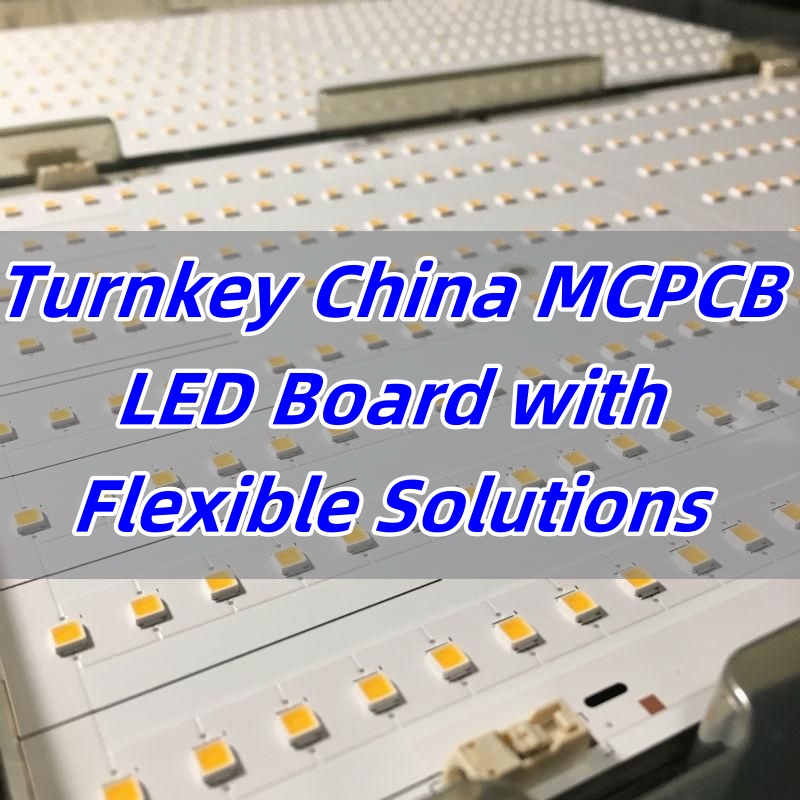
You may also like