PCB manufacturing PCB manufacturing
Home > Blog

12 Critical Materials and Components in the Semiconductor Supply Chain

August 20th, 2026

The semiconductor supply chain depends on far more than the chip itself. A semiconductor chip may be only a few millimeters across, but producing it depends on a surprisingly long chain of materials, chemicals, substrates, gases, passive components, and PCB materials. A shortage at almost any point in this chain can slow production even when wafer capacity itself is available.

That is why semiconductor supply-chain discussions should not focus only on silicon wafers. Materials such as photoresist, high-purity process gases, ABF substrates, copper foil, electronic-grade glass cloth, and passive components can become equally important bottlenecks.

The following 12 materials and components show how closely semiconductor fabrication, advanced packaging, PCB manufacturing, and electronics assembly are connected.

12 Critical Materials and Components in the Semiconductor Supply Chain

1. Indium Phosphide

Indium phosphide (InP) is a compound semiconductor material mainly used in high-frequency and optoelectronic devices.

It is commonly found in:

  • Optical communication systems
  • Photonic integrated circuits
  • Laser diodes
  • High-speed transistors
  • RF and microwave devices
  • Data-center optical modules

InP performs well in applications involving very high frequencies and light transmission.

Its supply chain is more specialized than conventional silicon. Crystal growth, wafer preparation, epitaxy, and device fabrication require dedicated processes, so production capacity cannot be expanded as easily as standard silicon manufacturing.

2. Photoresist

Photoresist in Semiconductor Manufacturing

Photoresist is a photosensitive material used during semiconductor lithography. A thin layer is coated onto the wafer and exposed through a patterned mask. After development, the remaining resist defines where later processes such as etching, deposition, or implantation will take place.

As circuit geometries shrink, photoresist must provide tight control over:

  • Resolution
  • Film uniformity
  • Sensitivity
  • Purity
  • Defect density
  • Line-edge accuracy

Photoresist is also used in PCB fabrication to define copper circuitry. The basic concept is similar, although semiconductor lithography operates at a much finer scale and under much stricter contamination requirements.

3. Silicon Carbide

Silicon Carbide in Power Electronics

Silicon carbide (SiC) is a wide-bandgap semiconductor material widely used in high-power electronics.

It is particularly suitable for systems that operate at high voltage, high temperature, or high switching frequency.

Typical applications include:

  • EV traction inverters
  • On-board chargers
  • DC-DC converters
  • Fast chargers
  • Solar inverters
  • Industrial motor drives
  • Data-center power supplies

SiC devices can reduce switching losses and improve power density, but manufacturing the wafers is difficult.

Crystal growth, slicing, polishing, epitaxy, and device processing all require precise control, which is one reason SiC supply has attracted attention as electric vehicles and power electronics expand.

4. Copper Foil

Copper foil is one of the core conductive materials used in PCB manufacturing.

After lamination and patterning, it becomes the board’s:

  • Signal traces
  • Power planes
  • Ground planes
  • Pads
  • Thermal structures

Copper thickness matters for current capacity, while surface roughness becomes especially important in high-frequency and high-speed designs.

Heavy copper boards need thicker copper for power handling and heat distribution. High-speed boards may require lower-profile copper to reduce conductor loss.

Although copper foil sounds like a basic material, its thickness, roughness, adhesion, and mechanical properties can directly affect PCB performance.

5. Tantalum Capacitors

Tantalum capacitors are electronic components rather than semiconductor raw materials, but they still matter in the wider electronics supply chain.

They are used where designers need relatively high capacitance in a compact package, including:

  • Power filtering
  • Industrial electronics
  • Telecom equipment
  • Aerospace systems
  • Medical devices
  • Automotive electronics

For PCBA production, a small passive component can become a bottleneck.

If a qualified tantalum capacitor is unavailable, replacing it may require checking voltage rating, capacitance, ESR, package size, reliability requirements, and approved alternatives before assembly can continue.

6. ABF Substrates

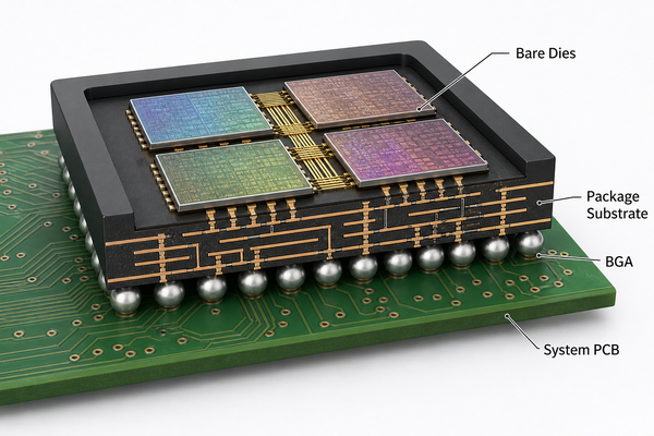
ABF substrates are widely used in advanced semiconductor packaging.

ABF stands for Ajinomoto Build-up Film, an insulating material used in high-density package substrates.

These substrates create the electrical connection between fine-pitch semiconductor packages and the larger interconnect structures on the PCB.

They are commonly associated with:

  • CPUs
  • GPUs
  • AI accelerators
  • Networking processors
  • High-performance computing devices

As package I/O density increases, substrate routing becomes finer and more complex.

Wafer capacity alone therefore does not determine how many finished chips can enter the market. Advanced packaging and substrate availability can become separate constraints.

7. High-Purity Nitrogen

Nitrogen is common in industry, but semiconductor manufacturing requires very high purity and controlled delivery.

It is used for:

  • Equipment purging
  • Oxygen displacement
  • Wafer handling
  • Chamber protection
  • Drying
  • Controlled process atmospheres

Semiconductor processes are highly sensitive to contamination, so trace moisture, particles, oxygen, or chemical impurities can affect process stability and yield.

High-purity nitrogen also has a place in electronics assembly. Nitrogen-assisted reflow and soldering processes may be used when oxidation control is important.

8. MLCCs

Multilayer ceramic capacitors, or MLCCs, are among the most common passive components on modern PCB assemblies.

They are used for decoupling, filtering, bypassing, and power stabilization.

Supply becomes more sensitive when a design combines demanding requirements such as:

  • Very small package sizes
  • High capacitance
  • Higher voltage
  • Automotive qualification
  • Tight tolerance
  • Specific temperature characteristics

An MLCC with the same nominal capacitance is not always a direct substitute.

Engineers may also need to review dielectric type, DC bias behavior, package size, voltage rating, temperature coefficient, and qualification requirements before approving an alternative.

9. Molybdenum Sputtering Targets

Molybdenum sputtering targets are used in physical vapor deposition processes.

During sputtering, atoms are released from the target and deposited as a thin film onto another surface.

For semiconductor and electronic applications, target quality depends on more than the molybdenum itself.

Manufacturers need to control:

  • Material purity
  • Density
  • Grain structure
  • Contamination
  • Dimensional consistency
  • Bonding quality

Minor impurities that are acceptable in ordinary industrial metal may create problems during high-precision thin-film processing.

Semiconductor-grade sputtering targets therefore belong to a highly controlled specialty-material supply chain.

10. Electronic-Grade Sulfuric Acid

Sulfuric acid is widely used in industry, but semiconductor production requires ultra-high-purity electronic-grade material.

It is used in wafer cleaning and other chemical processes where trace contamination must remain tightly controlled.

Key concerns include:

  • Metallic impurities
  • Particles
  • Organic contaminants
  • Ionic contamination

Producing industrial sulfuric acid and producing semiconductor-grade sulfuric acid are very different manufacturing tasks.

The purification system, packaging, transportation, handling, and quality controls all need to meet semiconductor processing requirements.

11. High-End PCB Substrates

After a semiconductor is packaged, it still needs a circuit board capable of supporting its electrical and thermal requirements.

Standard FR-4 is suitable for many products, but high-speed, RF, automotive, computing, and industrial designs may need laminates with tighter control over:

  • Dielectric constant
  • Dissipation factor
  • Tg
  • Thermal expansion
  • Moisture absorption
  • Dimensional stability
  • Copper adhesion

For these boards, material selection is part of the engineering process.

A laminate with similar mechanical specifications may behave very differently at multi-gigabit data rates or during repeated thermal cycling.

12. Electronic-Grade Glass Fiber Cloth

Electronic-grade glass fiber cloth is a reinforcement material used in many PCB laminates.

The cloth is impregnated with resin to form prepreg, which is then laminated with copper foil and core materials to build the PCB structure.

Important properties include:

  • Cloth thickness
  • Weave style
  • Yarn size
  • Resin impregnation
  • Dimensional stability
  • Surface uniformity

Glass weave can also affect high-speed signal behavior.

At very high data rates, traces passing over different glass and resin regions can experience small variations in effective dielectric properties. Material selection, routing strategy, and spread-glass constructions can help control this effect.

How Do Semiconductor Material Constraints Affect PCB and PCBA Production?

Before a finished electronic product can be built, the project depends on PCB materials, passive components, connectors, assembly materials, and manufacturing capacity.

Several materials discussed above connect directly with PCB and PCBA production:

  • Copper foil affects conductor construction and electrical performance.
  • Glass cloth and laminate systems influence PCB mechanical and dielectric properties.
  • MLCCs and tantalum capacitors affect BOM availability and assembly scheduling.
  • High-performance substrates become more important as signal speed and power density increase.

Sourcing and engineering therefore need to work together in complex PCB and PCBA projects, particularly when materials or components have limited qualified alternatives.

Which Materials Matter Most in PCB Manufacturing?
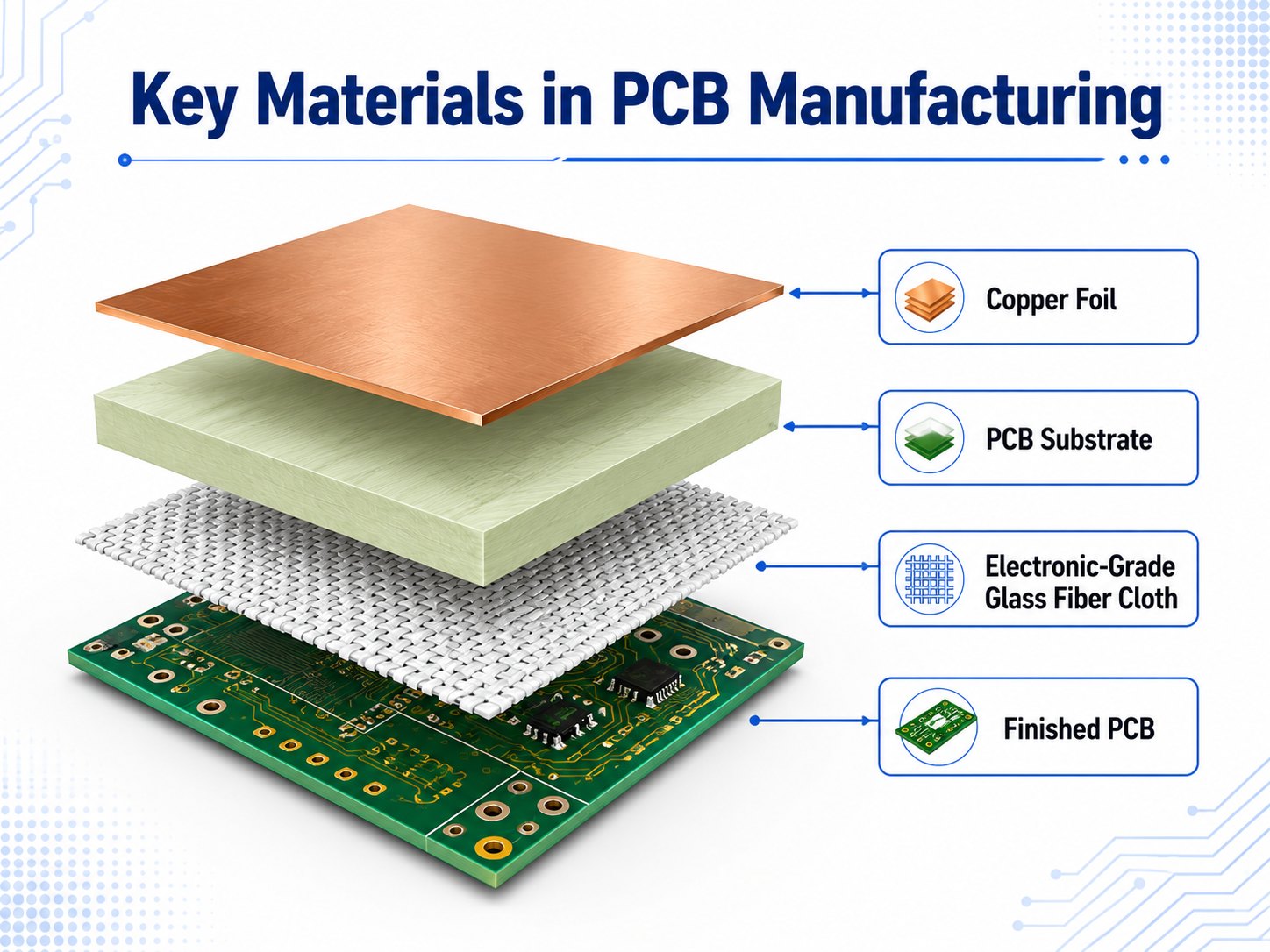
Key Materials in PCB Manufacturing

For PCB fabrication, the most relevant items from the list are copper foil, laminate materials, and electronic glass cloth.

Together, these materials define much of the board’s electrical, mechanical, and thermal behavior.

Engineers may need to evaluate:

  • Dk and Df
  • Tg and thermal stability
  • CTE
  • Copper thickness
  • Copper roughness
  • Moisture absorption
  • CAF resistance
  • Dimensional stability

These parameters become more important in HDI, RF, high-speed, high-current, heavy copper, automotive, and other demanding boards.

For example, low-loss laminate may matter far more than standard FR-4 in high-speed interfaces, while copper thickness and thermal design become central in high-current power boards.

How Do Component Shortages Affect PCBA Assembly?

How Component Shortages Affect PCBA Assembly

A bare PCB can be fully manufactured and still sit idle if critical BOM components are missing.

Component availability should therefore be reviewed early, especially for parts that are difficult to substitute.

Important checks include:

  • Manufacturer part number
  • Package and footprint
  • Lifecycle status
  • Lead time
  • Approved alternatives
  • Electrical specifications
  • Reliability grade
  • Supply continuity

Passive components deserve attention as well.

An MLCC or tantalum capacitor may look simple, but replacement can require engineering approval when voltage, dielectric behavior, package size, temperature performance, or qualification requirements differ.

How Can PCB and PCBA Buyers Reduce Supply-Chain Risk?

The practical approach is to identify critical materials and components before production starts.

For PCB projects, buyers should clearly define material, stack-up, copper thickness, impedance, surface finish, and any special thermal or reliability requirements.

For PCBA projects, the BOM should include accurate manufacturer part numbers and approved alternatives where possible.

Several steps can improve sourcing flexibility:

  • Perform DFM and BOM review early.
  • Approve equivalent PCB materials where technically acceptable.
  • Identify long-lead-time and single-source components.
  • Review alternative parts with engineering, not purchasing alone.
  • Separate ordinary BOM items from supply-critical parts.
  • Confirm material availability before mass production.

The goal is to avoid discovering a sourcing problem after production has already started.

How EBest Circuit Supports PCB and PCBA Manufacturing

How EBest Circuit Supports PCB and PCBA Manufacturing

At EBest Circuit, we support PCB and PCBA projects from engineering review and PCB fabrication through component sourcing, assembly, inspection, and testing.

Our PCB capabilities include:

  • Rigid PCB
  • Flex and rigid-flex PCB
  • HDI PCB
  • Heavy copper PCB
  • RF and microwave PCB
  • High-speed PCB
  • High-current PCB

For PCBA projects, EBest Circuit can also coordinate:

  • Component sourcing
  • SMT assembly
  • Through-hole assembly
  • Inspection
  • Testing

Before production, our engineering team can review key project information such as:

  • Gerber files
  • BOM
  • Pick-and-place data
  • PCB stack-up
  • Material requirements
  • Controlled impedance
  • Copper thickness
  • Assembly notes
  • Testing requirements

This allows PCB fabrication, component sourcing, and PCBA assembly requirements to be reviewed within the same project workflow.

Conclusion

These 12 materials and components show that semiconductor supply is closely tied to PCB and electronics manufacturing.

Some are used inside semiconductor fabrication. Others become important during advanced packaging, PCB production, component sourcing, and PCBA assembly.

For PCB and PCBA buyers, the practical issue is broader than chip availability. PCB materials, BOM components, fabrication requirements, assembly, and sourcing all need to align before a product can move smoothly into production.

If you have a PCB or PCBA project, send EBest Circuit your Gerber files, BOM, stack-up, and technical requirements for engineering review and quotation.

You may also like

Pull Up vs Pull Down Resistor: How to Choose the Right One

August 19th, 2026

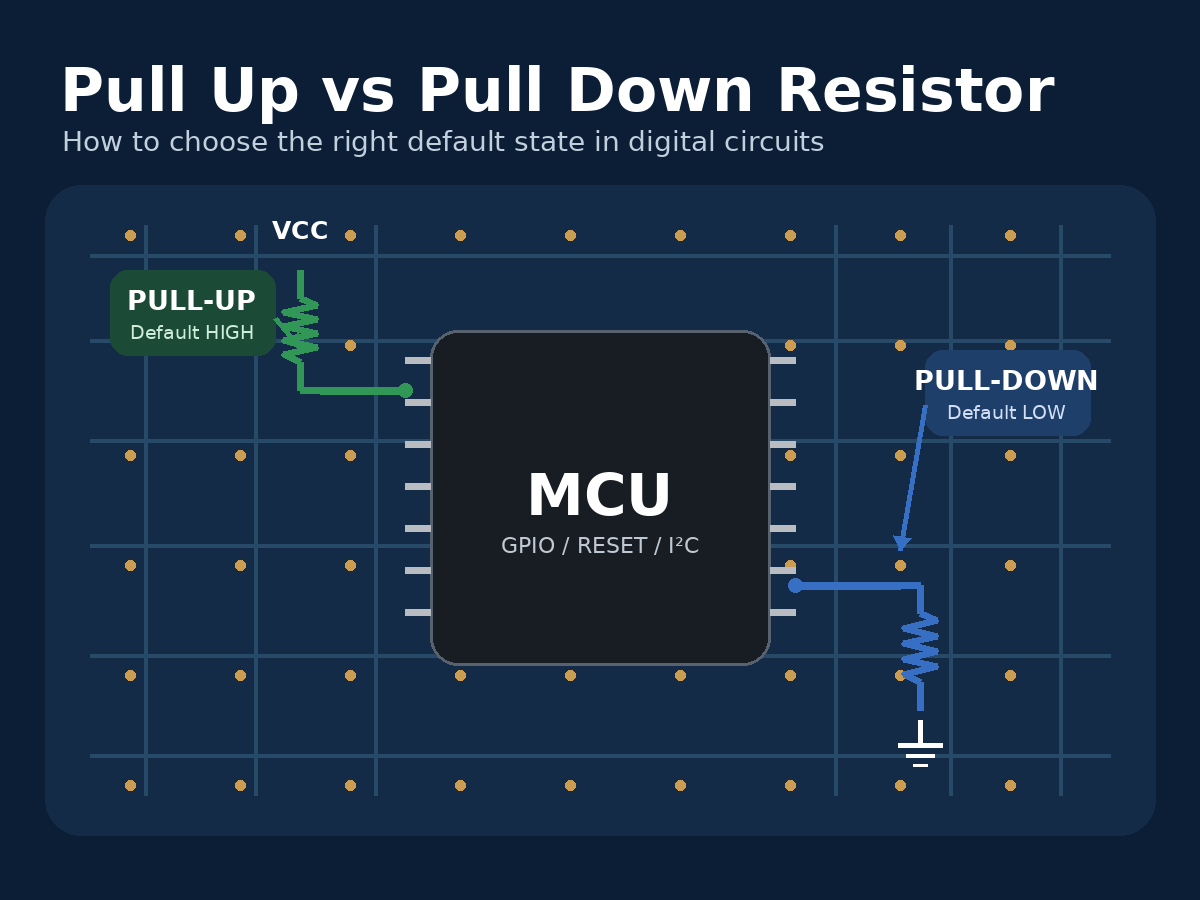
A pull up vs pull down resistor comparison comes down to one basic decision: what logic state should a signal have when no device is actively driving it? A pull-up resistor keeps the signal HIGH by connecting it to the positive supply through resistance, while a pull-down resistor keeps it LOW by connecting it to ground. Both prevent a high-impedance digital input from sitting at an undefined voltage.

The difference is simple, but choosing the right arrangement becomes more important in real circuits involving MCU GPIO, reset and enable pins, sensors, open-drain outputs, I²C buses, and power-up sequencing. This guide explains how pull-up and pull-down resistors work, when to use each type, how to select a suitable resistor value, and what engineers should check before a design moves from schematic to PCB production.

pull up vs pull down resistor

Pull Up vs Pull Down Resistor: What Is the Difference?

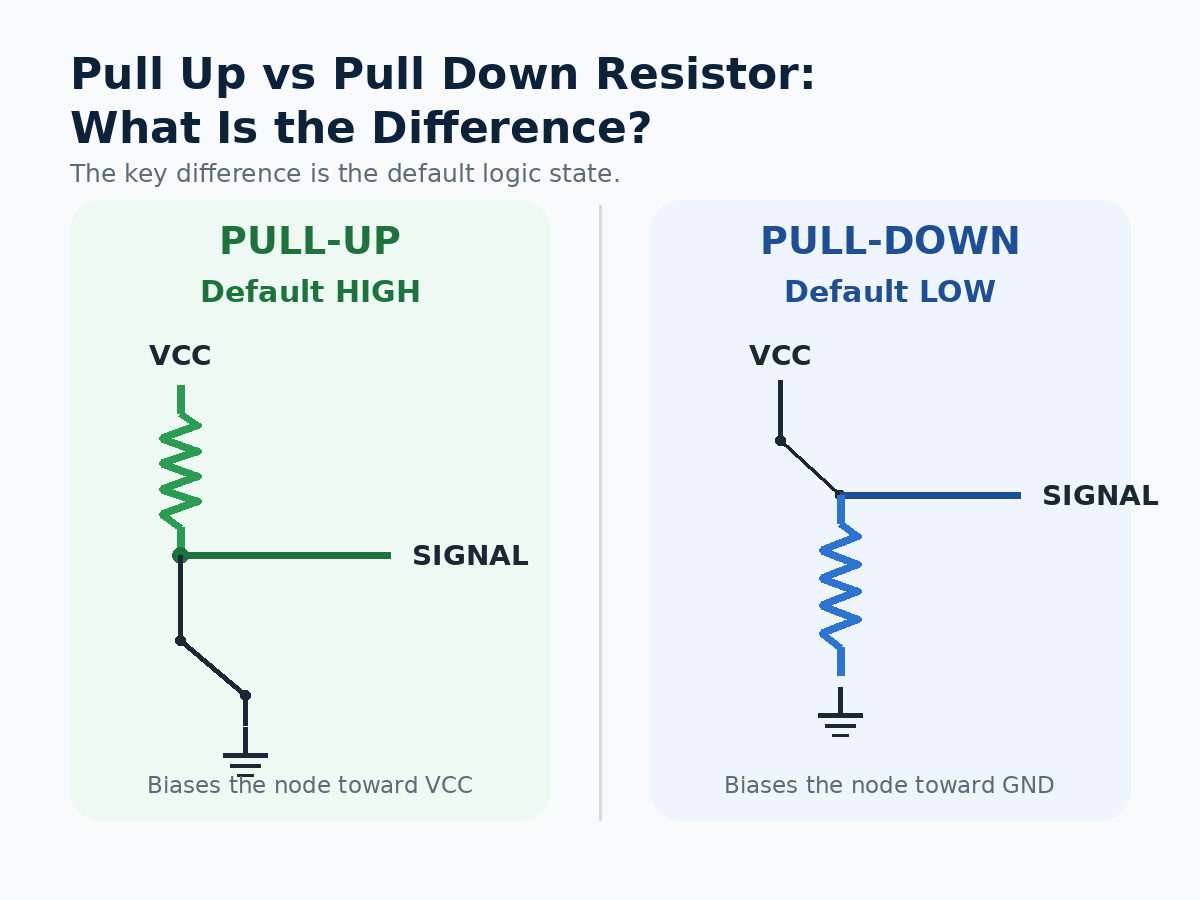
The main difference between pull-up and pull-down resistors is the default logic state they establish.

A pull-up resistor connects the signal to VCC, so an undriven input normally reads HIGH. A pull-down resistor connects the signal to ground, so the same type of input normally reads LOW.

Design PointPull-Up ResistorPull-Down Resistor
Resistor connectionSignal to VCCSignal to GND
Default logic stateHIGHLOW
Typical active stateLOWHIGH
Common switch connectionSignal to GNDSignal to VCC
Common usesOpen-drain signals, reset lines, interrupts, MCU inputsEnable pins, gate control, default-low inputs
Logic behaviorOften active-lowOften active-high

Neither method is inherently better. The correct choice depends on what the circuit should do when the switch, controller, or external signal is inactive.

A useful first rule is:

Default HIGH → use a pull-up.
Default LOW → use a pull-down.

For open-drain or open-collector signals, a pull-up is normally required because the output can actively pull the line LOW but cannot actively drive it HIGH.

pull up vs pull down resistor

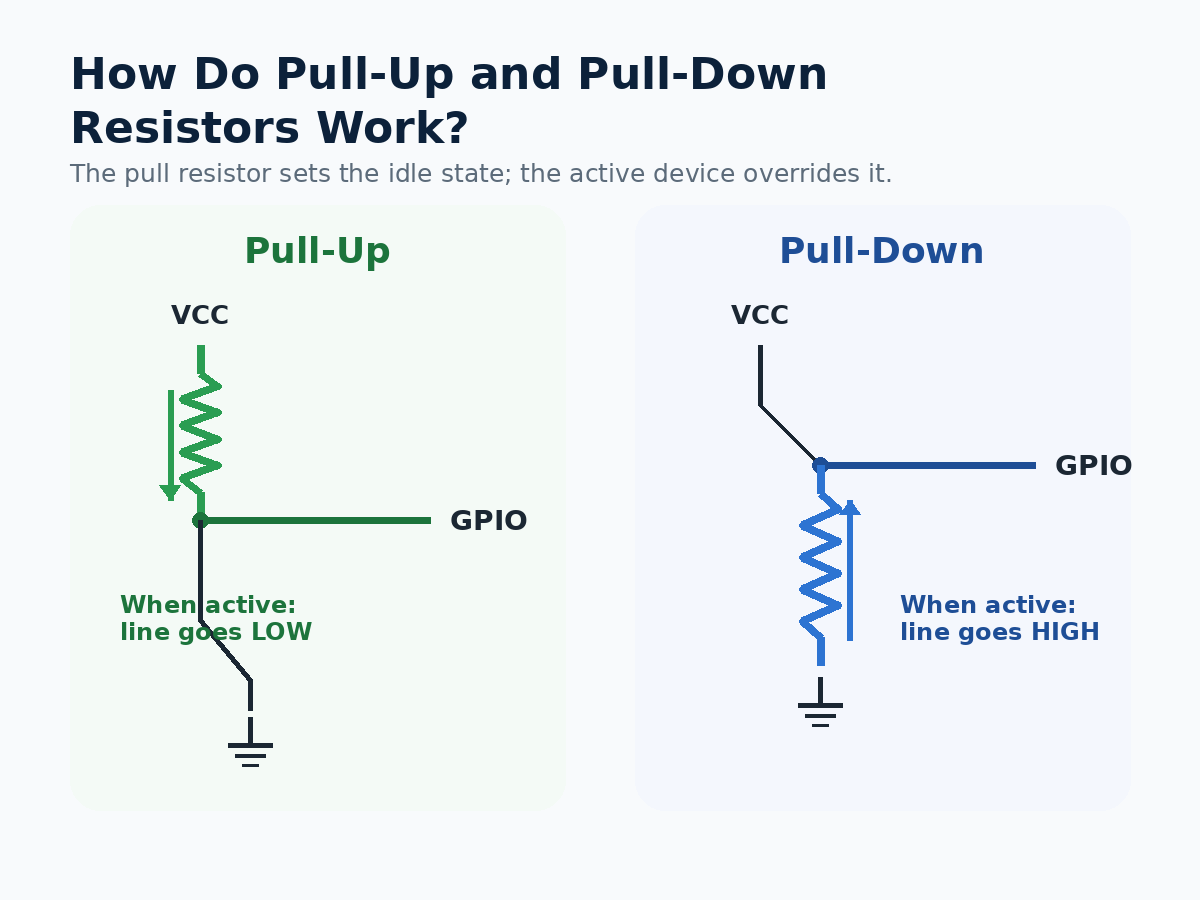
How Do Pull-Up and Pull-Down Resistors Work?

Pull-up and pull-down resistors provide a weak connection to one power rail while allowing another device to override that state.

Pull-up resistor circuit

A pull up resistor circuit typically connects:

VCC → resistor → signal node

A switch, transistor, or open-drain output can then connect the signal node to ground.

When nothing drives the line, the resistor brings the node toward VCC. When the signal is pulled to ground, the resistor limits the current between VCC and GND.

For example, with a 3.3 V supply and a 10 kΩ resistor:

I = V / R = 3.3 / 10,000 ≈ 0.33 mA

Pull-down circuit

A pull down circuit reverses the arrangement:

Signal node → resistor → GND

An external source can then drive the node toward VCC. When that source is removed, the resistor brings the signal back toward ground.

The resistor therefore does two jobs: it establishes a known idle voltage and limits current when another device drives the line in the opposite direction.

This is why simply connecting a signal directly to VCC or GND is not equivalent to using a pull resistor. A direct connection could create excessive current when another device attempts to drive the opposite state.

pull up vs pull down resistor

Why Are Pull-Up and Pull-Down Resistors Needed?

Digital inputs often have very high input impedance. If an input is disconnected and has no pull-up or pull-down path, it can become a floating input.

A floating node may respond to leakage current, residual charge, nearby switching signals, EMI, or capacitive coupling. The voltage can move between valid HIGH and LOW thresholds instead of remaining at a predictable level.

That can create behavior such as:

  • an MCU input changing state without a valid command;
  • a reset or enable pin activating unexpectedly;
  • a MOSFET control node entering an unintended state;
  • intermittent sensor or digital-interface behavior;
  • unstable operation during startup or controller reset.

The startup condition deserves particular attention in production electronics. Firmware does not configure every GPIO immediately when power is applied. An external pull resistor can establish the required state before firmware runs.

For example, an enable pin that must remain inactive during power-up may use a pull-down resistor even if the microcontroller later controls that signal directly.

Pull resistors are therefore not merely “logic accessories.” They help define circuit behavior during the moments when no active driver is in control.

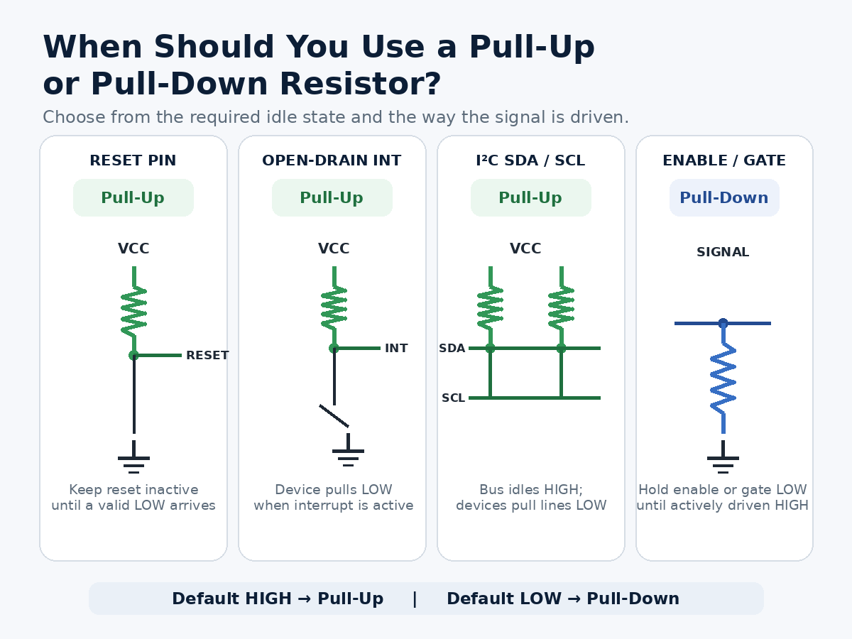
When Should You Use a Pull-Up or Pull-Down Resistor?

The easiest way to choose between them is to start with the required idle state and then check how the active device drives the signal.

Use a pull-up resistor when:

  • the signal should default HIGH;
  • a switch or transistor pulls the line toward ground;
  • the signal is active-low;
  • an open-drain or open-collector output is used;
  • reset, interrupt, or chip-select lines should remain HIGH when inactive;
  • a communication interface requires a passive HIGH state.

Use a pull-down resistor when:

  • the signal should default LOW;
  • an external device drives the node toward VCC;
  • an enable pin must remain disabled during startup;
  • a transistor or MOSFET control input should stay off until commanded;
  • a disconnected external input should be interpreted as logic 0.

Open-drain buses are a particularly important case. I²C SDA and SCL lines, for example, are normally pulled HIGH through resistors while connected devices pull them LOW when transmitting.

The decision should also consider power-up behavior. If the correct logic state must exist before the MCU initializes, relying only on firmware configuration may not be sufficient.

In other words, choose the resistor according to what the hardware must do when software is not yet in control.

pull up vs pull down resistor

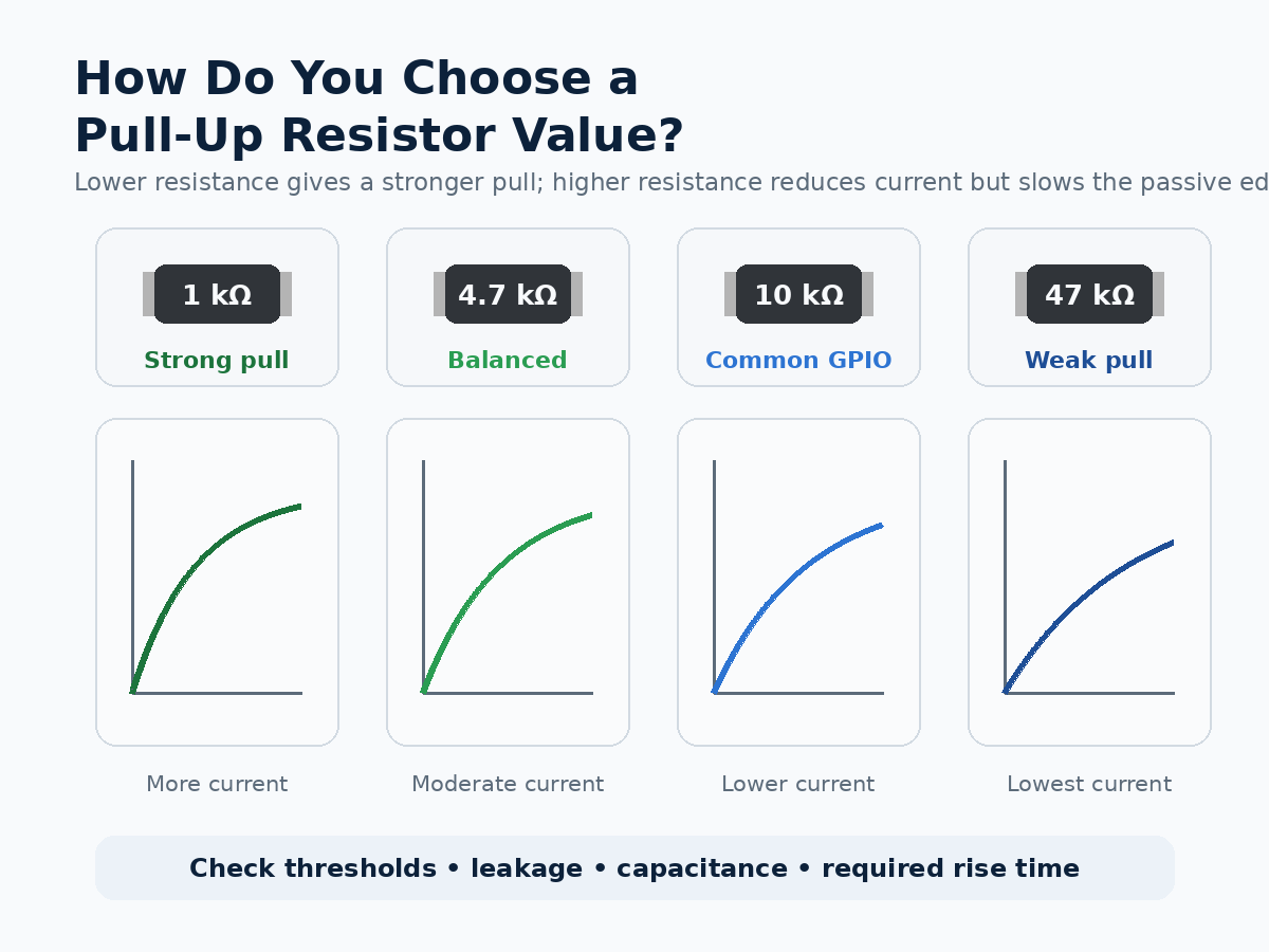
How Do You Choose a Pull Up Resistor Value?

There is no universal pull up resistor value. 10 kΩ is common in slow digital-input circuits, but it should be treated as a starting point rather than a default engineering rule.

The value should be selected by checking four main factors:

  • Logic thresholds: the resulting voltage must remain inside the valid HIGH or LOW region specified by the IC.
  • Leakage current: a very high resistance can allow device leakage to shift the signal away from the intended level.
  • Current consumption: a lower resistance creates a stronger pull but increases current when another device drives the opposite state.
  • Capacitance and switching speed: resistance combines with line and input capacitance to form an RC network. Higher resistance generally produces slower passive transitions.

Typical values illustrate the tradeoff:

Resistor ValueGeneral BehaviorTypical Consideration
1 kΩStrong pull, faster edgeHigher active-state current
4.7 kΩModerate pullCommon compromise in many digital circuits
10 kΩLower currentOften suitable for low-speed GPIO
47 kΩ or higherVery low currentMore sensitive to leakage, noise, and capacitance

These are examples, not universal design values.

For I²C and other open-drain interfaces, resistor selection requires particular care because bus capacitance and rise-time limits directly affect the acceptable resistance range.

For a production PCB, the better approach is to check the IC datasheet and interface specification rather than copying a resistor value from another schematic.

pull up vs pull down resistor

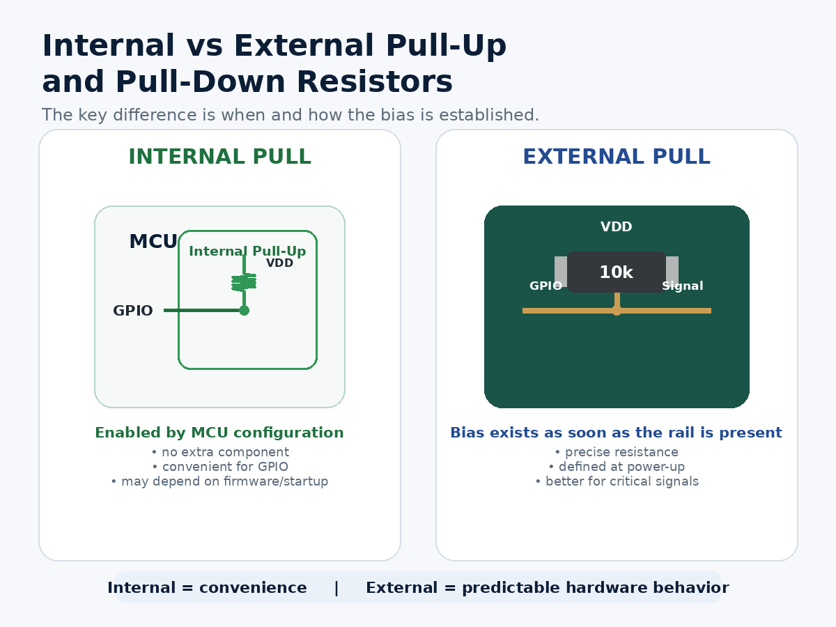
Internal vs External Pull-Up and Pull-Down Resistors

Many microcontrollers provide configurable internal pull-up and sometimes pull-down resistors. These are convenient because they reduce component count and can be enabled through the GPIO configuration.

Internal resistors are often sufficient for:

  • simple buttons and switches;
  • configuration straps;
  • low-speed GPIO inputs;
  • non-critical digital signals where the exact resistance is not important.

External resistors provide more design control.

Internal Pull ResistorExternal Pull Resistor
No additional componentRequires PCB and BOM space
Convenient for GPIOResistance can be selected precisely
Enabled by firmware/configurationCan define state immediately at power-up
Resistance may vary more widelyBetter control of current and RC timing
Good for many low-speed inputsBetter for interfaces with defined electrical requirements

The most important difference in a real product is often when the pull becomes active.

An external resistor works as soon as the relevant power rail is present. An internal resistor may not become active until the MCU reaches a particular startup state or firmware configures the GPIO.

That distinction matters for reset pins, power enables, safety-related control signals, and circuits where another IC becomes active before the main controller.

External components are also usually preferable when rise time, leakage margin, interface compliance, or resistance tolerance must be engineered rather than simply accepted.

pull up vs pull down resistor

How Are Pull-Up and Pull-Down Resistors Used in Microcontroller Circuits?

A pull up resistor in microcontroller designs can appear in many places beyond a simple pushbutton.

Common MCU applications include:

GPIO inputs.

  • A pull resistor keeps an unused or externally controlled input at a defined level until another circuit changes it.

Reset and enable pins.

  • Pull resistors establish a safe startup condition before firmware begins controlling the board.

Interrupt signals.

  • Many sensors and peripheral ICs use open-drain interrupt outputs, making a pull-up necessary to create the HIGH state.

I²C communication.

  • SDA and SCL use open-drain signaling and require pull-ups whose values suit the operating voltage, bus capacitance, and required rise time.

Configuration pins.

  • Pull-up or pull-down resistors can define boot modes, addresses, or operating states when the system powers on.

Arduino provides a familiar example. INPUT_PULLUP allows supported microcontrollers to enable an internal pull-up for a GPIO input, so a pushbutton can connect between the pin and ground. In that arrangement, the unpressed state reads HIGH and the pressed state reads LOW.

For production MCU boards, however, engineers usually need to look beyond the basic pull up resistor Arduino example. Startup timing, external peripherals, power domains, leakage, signal speed, and what happens before firmware executes can all determine whether an internal resistor is sufficient or an external component is the safer choice.

Common Pull-Up and Pull-Down Resistor Mistakes

Pull resistors are simple components, which makes them easy to overlook during schematic and PCB review. Many problems come from treating a familiar value or reference design as universally applicable.

Common mistakes include:

  • Leaving high-impedance inputs floating. An unused or externally disconnected input may need a defined bias rather than being left open.
  • Using 10 kΩ automatically. A familiar value can still be too weak, too slow, or unnecessarily strong for a particular circuit.
  • Ignoring startup behavior. An internal MCU pull may not control the signal during the earliest stage of power-up.
  • Forgetting active-low logic. With a pull-up switch input, the active condition may read LOW rather than HIGH.
  • Ignoring bus capacitance. On open-drain interfaces such as I²C, excessive resistance can produce slow rising edges.
  • Using the wrong BOM or population option. A schematic may show optional pull resistors while the production BOM or assembly drawing specifies a different DNP/populated condition.

The final check should therefore extend beyond the schematic symbol. Confirm the resistor value, voltage rail, logic polarity, startup condition, populated/DNP status, and interface requirements.

For MCU, sensor, control, and embedded PCBs, these checks are especially useful before fabrication because a small biasing error can otherwise appear later as an intermittent communication, startup, or functional-test problem.

FAQs About Pull Up vs Pull Down Resistor

Can a signal have both a pull-up and a pull-down resistor?

Yes, but the two resistors then form a voltage divider. The resulting voltage depends on their resistance ratio, so this arrangement should only be used when that intermediate bias level is intentional.

Do output pins need pull-up or pull-down resistors?

A normal push-pull output usually drives both HIGH and LOW actively, so it does not need a pull resistor for basic operation. Open-drain or open-collector outputs are different because they typically require a pull-up to create the HIGH state.

Is a 10 kΩ pull-up resistor suitable for every digital input?

No. 10 kΩ is useful in many low-speed circuits, but leakage current, logic thresholds, capacitance, switching speed, and power requirements can make another value more appropriate.

Can pull-up resistors be used with both 3.3 V and 5 V circuits?

Yes, provided the resistor connects to a voltage that is valid for every device on that signal. The pull-up voltage must not exceed the input-voltage limit of any connected IC.

Should an external pull resistor be added if the MCU already has an internal one?

Not necessarily. Internal pulls are convenient for many GPIO inputs, but an external resistor is preferable when the signal needs a defined state before firmware initialization, a specific resistance, stronger biasing, or controlled rise time.

If your MCU, sensor, industrial control, or embedded design is moving from schematic to production, you can send the Gerber/PCB files, BOM, and project requirements to sales@bestpcbs.com. EBest Circuit can support engineering review, PCB fabrication, component sourcing, PCBA assembly, testing, and quotation for the next production stage.

You may also like

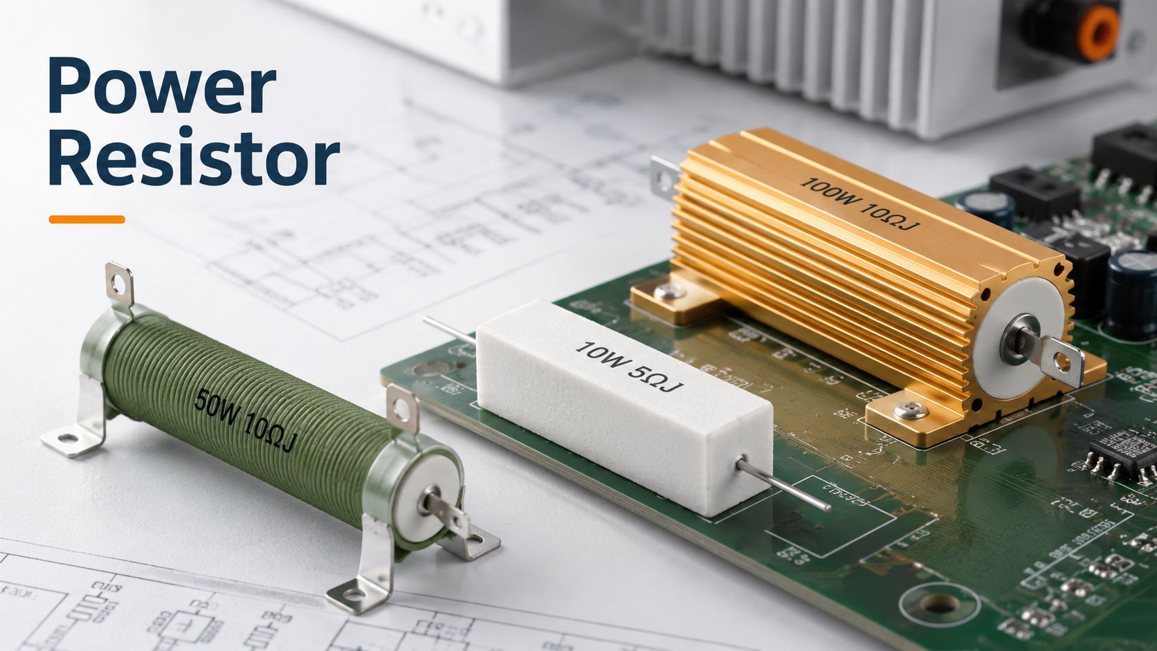
Power Resistor: How It Works and How to Choose One

August 19th, 2026

A power resistor is used when a circuit needs to dissipate more electrical energy than a standard signal-level resistor can comfortably handle. These components are common in power supplies, motor drives, battery systems, inverters, charging equipment, and industrial controls, where current, voltage, or transient energy can generate substantial heat.

Choosing the right power resistor involves more than matching the resistance value. Power rating, working voltage, pulse capability, operating temperature, construction, and mounting conditions all affect performance. This guide explains how power resistors work and what to consider when selecting one for a real circuit.

power resistor

What Is a Power Resistor?

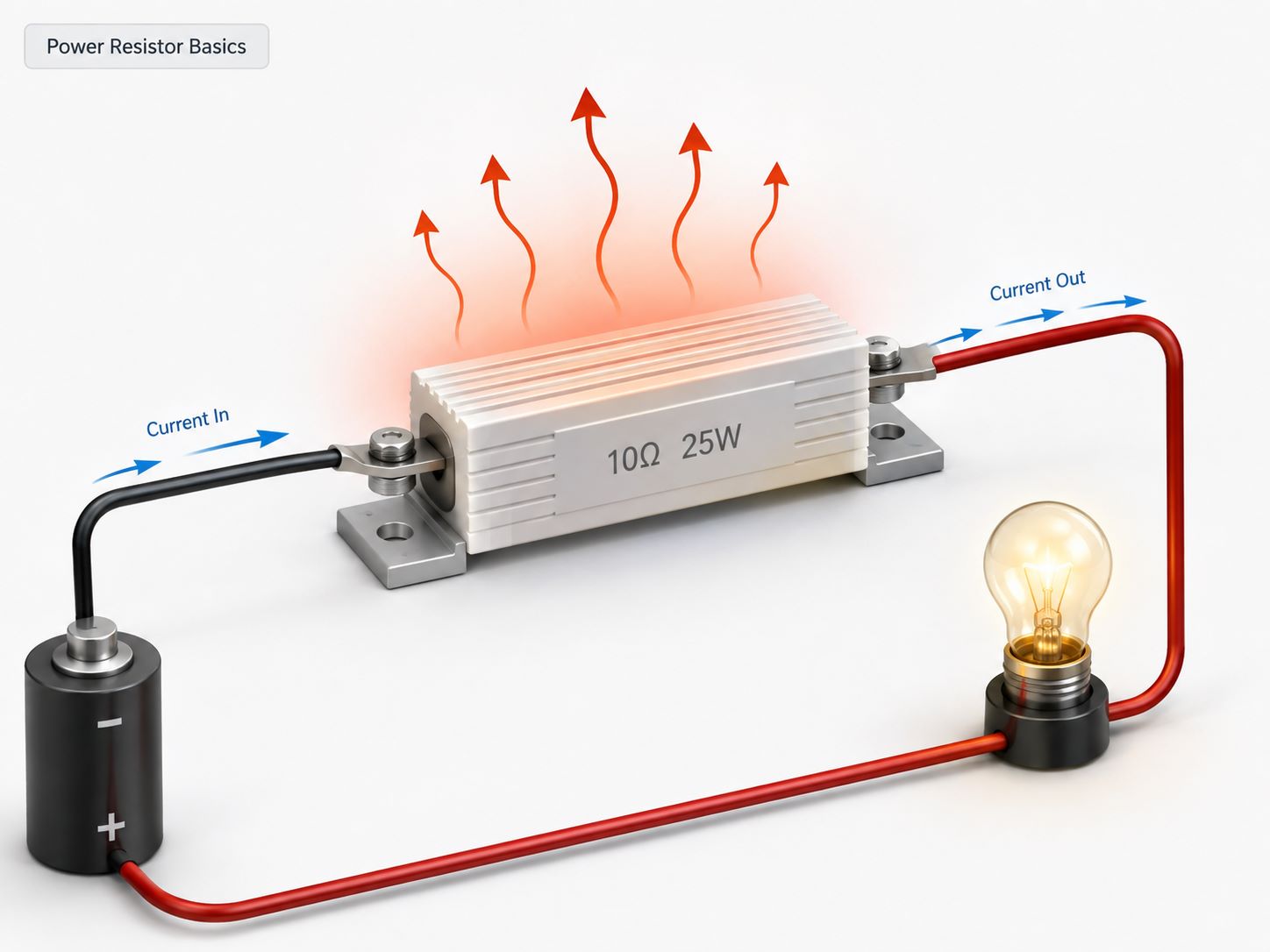
A power resistor is a resistor designed to dissipate relatively large amounts of electrical power as heat while maintaining its specified resistance.

Like other resistors, it limits current or creates a controlled voltage drop. The main difference is its ability to manage a higher thermal load.

The basic power relationships are:

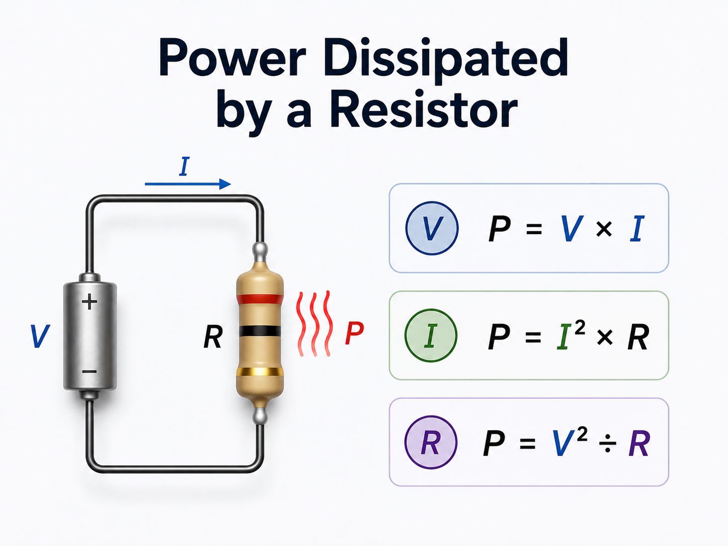
  • P = V × I
  • P = I² × R
  • P = V² ÷ R

Where P is power, V is voltage, I is current, and R is resistance.

For example, if 2 A flows through a 10 Ω resistor:

P = 2² × 10 = 40 W

The resistor must therefore manage about 40 W of heat under that operating condition.

This does not mean a 40 W resistor should automatically be selected. Continuous operation near the maximum rating may leave little thermal margin, especially inside a warm enclosure or without sufficient airflow.

Power resistors use different constructions to move heat away from the resistive element. Depending on the component, heat may be released into the surrounding air, transferred through the PCB, or conducted into a chassis or heatsink.

power resistor

When to Use a High Power Resistor?

A high power resistor is appropriate when continuous power, pulse energy, or operating temperature exceeds what a conventional resistor can safely handle.

There is no universal wattage at which a resistor becomes “high power.” The required rating depends on the application.

Typical situations include:

  • capacitor discharge;
  • inrush current limiting;
  • motor braking;
  • load testing;
  • current limiting;
  • repeated pulse absorption;
  • high-temperature operation.

A higher wattage rating does not cause a resistor to consume more power. Circuit conditions determine the actual dissipation.

For example, a 100 Ω resistor with 10 V across it dissipates:

P = 10² ÷ 100 = 1 W

A 2 W, 5 W, or 20 W version would still dissipate approximately 1 W in the same circuit. The higher-rated resistor simply provides more thermal capacity.

When choosing a high wattage resistor, however, wattage should not be the only consideration. Maximum working voltage, pulse rating, inductance, physical size, and mounting method can be equally important.

For switching circuits or repetitive pulses, check the manufacturer’s overload or pulse-energy data rather than relying only on the continuous power rating.

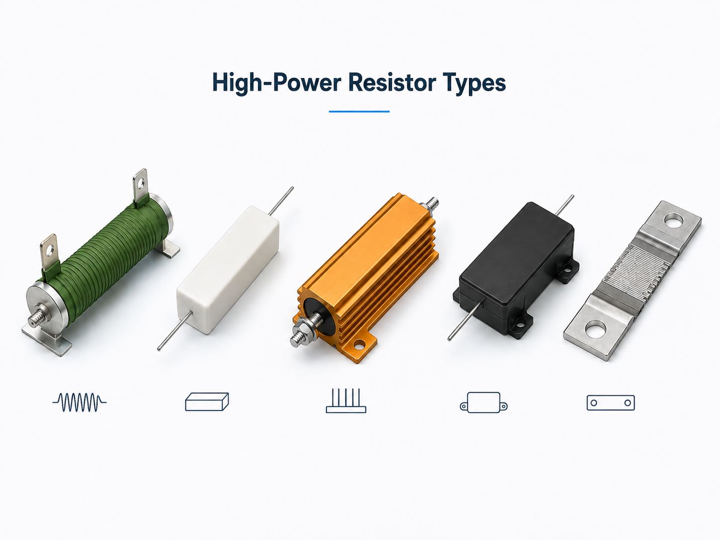
Which Type of Resistor Is Used for High Power Applications?

The best resistor for a high-power application depends on continuous wattage, pulse energy, available space, required precision, and thermal conditions.

Wirewound resistors

  • Wirewound resistors offer good power handling and overload capability. They are widely used in motor drives, power supplies, braking systems, and load banks. Their wound construction can introduce inductance, so low-inductance designs may be preferred in fast-switching circuits.

Ceramic or cement resistors

  • A ceramic resistor or cement resistor provides a robust and economical option for current limiting, discharge circuits, snubbers, and general power electronics.

Aluminum-housed resistors

  • These resistors transfer heat efficiently into a chassis or heatsink. They are useful when relatively high continuous power must be handled in a compact space.

Thick-film power resistors

  • Thick-film designs can combine compact size, relatively high resistance values, and low inductance, making them useful in modern power electronics.

Foil resistors

  • A foil resistor is more suitable when power handling must be combined with tight tolerance or low temperature coefficient.

There is therefore no single answer to which type of resistor is used for high power applications. The correct choice depends on whether the main design constraint is heat, pulse energy, precision, size, or high-frequency behavior.

power resistor

What Is a Resistor Power Rating?

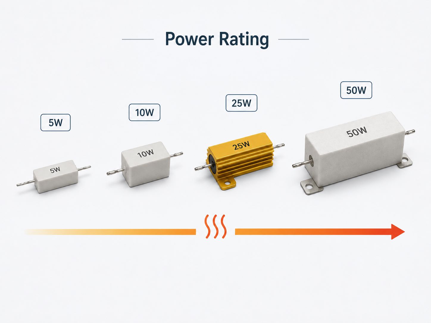
A resistor power rating indicates how much electrical power a resistor can dissipate under specified conditions without exceeding its allowable temperature.

Power ratings are normally expressed in watts. Common values range from fractions of a watt to tens, hundreds, or even thousands of watts for industrial resistor assemblies.

A 50 W resistor rated power, however, does not necessarily mean the component can continuously dissipate 50 W under every condition.

The published rating may assume:

  • a defined ambient or case temperature;
  • sufficient airflow;
  • a particular PCB layout;
  • mounting on a metal chassis;
  • installation on a specified heatsink.

As temperature increases, allowable power usually decreases. This relationship is shown in the manufacturer’s derating curve.

A practical selection should therefore satisfy:

Actual power dissipation < Allowable power under real operating conditions

The nominal wattage is only the starting point.

Continuous-load designs should also leave suitable thermal margin, while pulse applications require separate verification of pulse duration, repetition rate, and overload capability. A resistor that can dissipate 50 W continuously is not automatically suitable for every short high-energy pulse.

power resistor

How to Calculate Power Dissipated by a Resistor?

The power dissipated by a resistor can be calculated from voltage, current, and resistance.

Use the equation that matches the values already known:

  • P = V × I
  • P = I² × R
  • P = V² ÷ R

For example, if a 20 Ω resistor carries 1.5 A:

P = 1.5² × 20 = 45 W

This means the resistor dissipates about 45 W.

This power resistor formula works well for steady DC conditions. Pulsed loads require an additional check because average power does not fully describe short-duration thermal stress.

For pulse applications, consider:

  • peak power;
  • pulse width;
  • repetition frequency;
  • duty cycle;
  • pulse energy.

A resistor may experience very high instantaneous power for a few milliseconds while still showing a much lower average wattage.

For this reason, repetitive pulse applications should be checked against the manufacturer’s pulse-power or pulse-energy curves. This is particularly important in precharge circuits, capacitor discharge systems, motor drives, and switching power supplies.

For steady loads, calculate the actual resistor power first. For pulsed loads, calculate the power and then verify whether the resistor construction can survive the pulse profile.

power resistor

Do Resistors Have Voltage Ratings?

Yes. Resistors do have voltage ratings, and the voltage limit can become important even when power dissipation remains within the resistor’s wattage rating.

Power and voltage ratings describe different design limits.

For example, a high-resistance component may carry very little current, so its calculated power remains low. At the same time, a high voltage across the resistor may exceed its maximum working-voltage specification.

The voltage associated with resistance and power can be estimated using:

V = √(P × R)

However, the result still needs to be compared with the manufacturer’s specified maximum working voltage.

In practice, the lower limit governs:

  • voltage allowed by the power rating; or
  • specified maximum working voltage.

High-voltage designs should also consider PCB creepage and clearance, terminal spacing, resistor body construction, contamination, and transient voltage.

When a single resistor cannot withstand the required voltage, several resistors may be connected in series to distribute the voltage stress, provided their power and voltage ratings are both checked.

What Are Power Resistors Used For?

Power resistors are used when electrical energy needs to be limited, discharged, measured, controlled, or converted into heat.

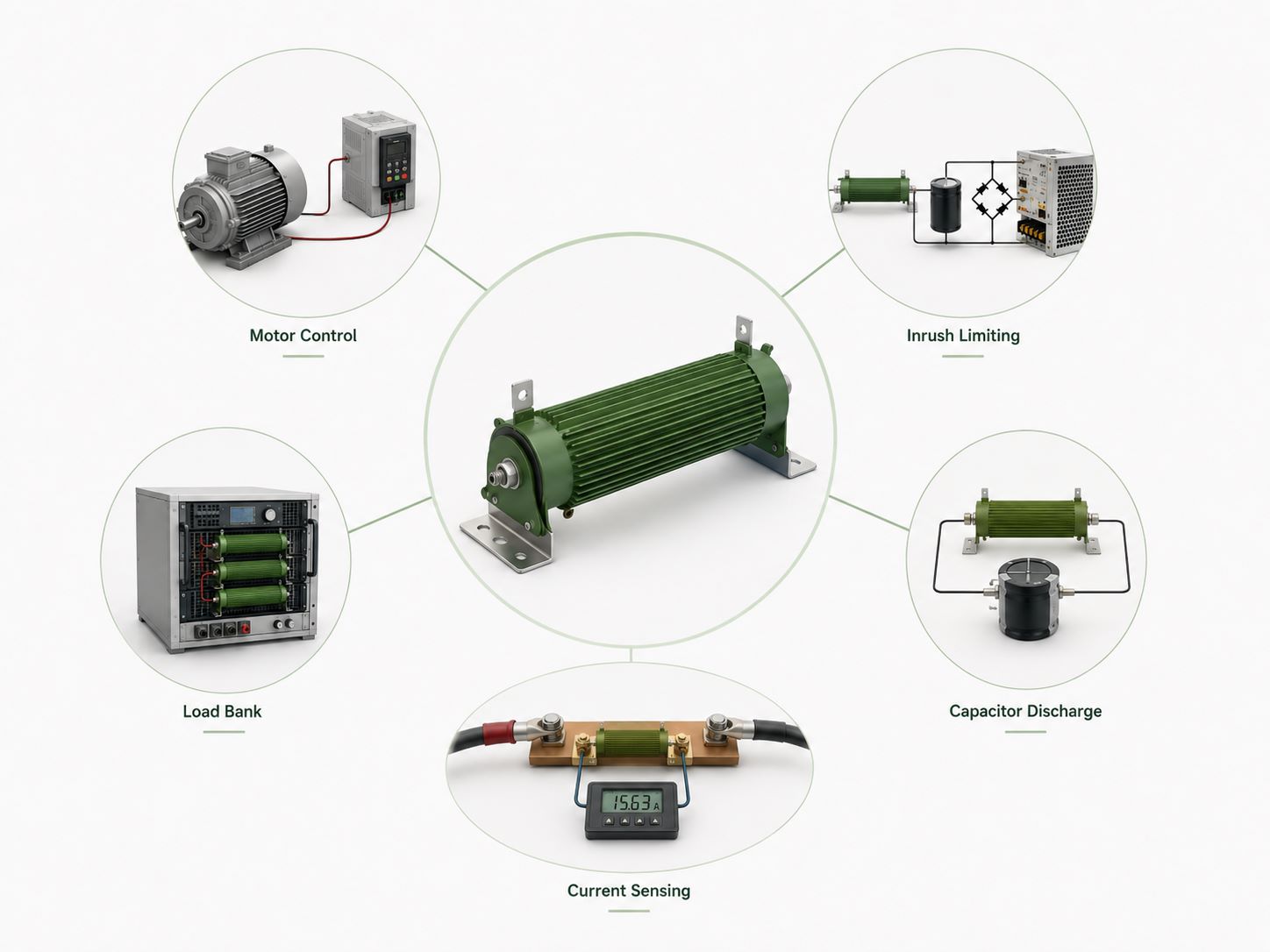
Common power resistor applications include:

Motor braking

  • Braking resistors dissipate regenerated energy when a motor decelerates, helping control the DC bus voltage.

Inrush current limiting

  • A resistor can temporarily limit the high current drawn when large capacitors are first charged.

Capacitor discharge

  • Bleeder and discharge resistors remove stored energy from capacitors after power is disconnected.

Power supplies

  • Power resistors can provide minimum loading, voltage balancing, current limiting, and controlled energy dissipation.

Snubber and damping circuits

  • Resistors may work with capacitors to suppress ringing or absorb switching transients.

Load banks

  • Industrial resistors are commonly used to create controlled loads for testing batteries, generators, chargers, converters, and power supplies.

Current sensing

  • Low-resistance power resistors can act as shunts, producing a small voltage proportional to current.

The required resistor construction changes with the application. A braking resistor prioritizes energy and heat handling, while a current-sense resistor may prioritize low resistance, accuracy, and temperature stability.

power resistor

Can I Use a Higher Wattage Resistor?

Yes, in many circuits a higher-wattage resistor can replace a lower-wattage resistor when the other specifications remain suitable.

For example, a 100 Ω, 5 W resistor can often replace a 100 Ω, 2 W resistor. If the circuit produces 1 W of dissipation, the 5 W component still dissipates approximately 1 W. Its higher rating simply provides additional thermal margin.

Before using a higher wattage resistor, check:

  • resistance value;
  • tolerance;
  • maximum working voltage;
  • pulse rating;
  • temperature coefficient;
  • inductance;
  • physical size;
  • mounting requirements.

This matters because two resistors with the same resistance but different wattage ratings may use different constructions.

A larger wirewound resistor, for example, may introduce more inductance than a smaller low-inductance component. A chassis-mounted resistor may also achieve its published power rating only when installed on an appropriate metal surface.

So, can I use a higher wattage resistor? Usually yes—but wattage should not be considered in isolation.

Choose enough power margin for the real operating environment without unnecessarily increasing size, cost, or parasitic effects.

FAQs About Power Resistor

Is it normal for a power resistor to get very hot?

Yes. Power resistors convert electrical energy into heat, so high surface temperature can be normal. Check the datasheet temperature limit and derating curve rather than judging by touch alone.

How much wattage margin should I leave when choosing a power resistor?

There is no fixed margin for every design. Calculate the actual dissipation first, then select a resistor with enough headroom based on ambient temperature, cooling, duty cycle, and the manufacturer’s derating data.

Can I use several lower-wattage resistors instead of one high-power resistor?

Yes. Series, parallel, or series-parallel networks can share the load, provided the total resistance is correct and each resistor stays within its own power and voltage limits.

Can a power resistor briefly exceed its continuous wattage rating?

Sometimes. Short pulses may exceed the continuous rating if the resistor’s pulse or overload specification allows it. Always check pulse width, energy, repetition rate, and the manufacturer’s pulse curve.

Does a power resistor need a heatsink?

Not always. Some power resistors work in free air, while aluminum-housed or chassis-mounted types may need a heatsink or metal surface to achieve their rated power.

Planning a Power Resistor PCB or PCBA Project? If your project involves power resistors, high-current circuits, thermal design, or PCBA assembly, our engineering team can review your PCB files, BOM, and key requirements before production. You are also welcome to visit our factory to see our PCB and PCBA manufacturing process, production lines, and quality control in person. Send your project details or arrange a factory visit at sales@bestpcbs.com.

You may also like

Shunt Resistor Selection and PCB Layout for Accurate Sensing

August 18th, 2026

A shunt resistor circuit can be correct on the schematic and still produce inconsistent readings on assembled boards. At milliohm resistance levels, the PCB copper, pad entry, solder joints, temperature, and measurement nodes can contribute error that the basic calculation never shows.

The safest approach is to treat the shunt resistor, PCB layout, BOM, and acceptance test as one measurement system. This guide shows what to calculate, what to inspect in the layout, what to lock before purchasing, and what evidence to request from the PCBA build.

shunt resistor

What Is a Shunt Resistor?

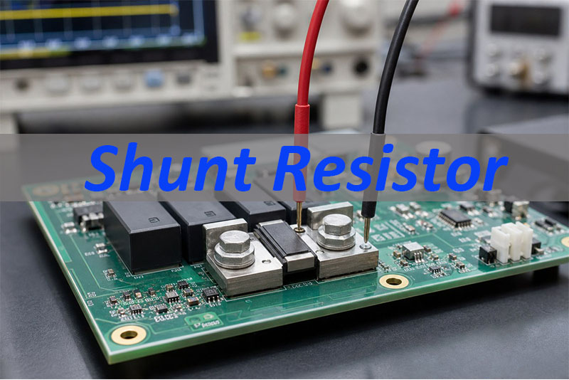
A shunt resistor, also called a current sense resistor, is a low-value resistor placed in the load-current path. Using a shunt resistor for measuring current is straightforward in principle: current creates a proportional voltage across the part. The voltage across it is proportional to current: V = I × R. A current-sense amplifier or ADC reads that voltage and converts it into a measurement or protection decision.

At 1 mΩ, every ampere produces only 1 mV. That makes the physical sense points important: copper, pads, solder joints, and amplifier offset can become a meaningful share of the signal. A precise component does not guarantee a precise assembled measurement.

Define three groups of requirements before selecting the part:

  • Electrical range — minimum, normal, maximum, surge, and fault current.
  • System limits — permitted voltage drop, power loss, response time, and accuracy over temperature.
  • Architecture — high-side or low-side sensing and a two-terminal or four-terminal shunt.

How Does Shunt Resistor Current Measurement Work?

A 2 mΩ shunt carrying 30 A gives three immediate results:

  • 60 mV across the shunt — confirm that the load can tolerate this voltage loss.
  • 1.8 W in the resistor — verify the derated thermal capacity in the real enclosure.
  • 2.4 V after a gain of 40 — confirm amplifier and ADC headroom, including faults and tolerances.

Accuracy must then be checked as a chain. Resistor tolerance sets the starting error. Temperature coefficient changes the resistance as the part heats. Amplifier offset becomes significant when the sense voltage is small. Gain error, ADC reference error, noise, and any copper included between the real sense points add further uncertainty.

Do not specify accuracy only at room temperature and nominal current. Define at least a low-current point, a normal operating point, and a high-current point after thermal stabilization. If the circuit also protects against faults, add the trip current, response time, and allowed recovery behavior. These become the basis of calibration and production testing.

Use the symptom to narrow the cause. A large percentage error at low current usually points first to offset, noise, or incorrect sense points. Drift that appears only after high-current warm-up points more strongly to shunt TCR, temperature rise, or heated copper. A consistent gain error across the range may be calibratable; unstable board-to-board variation usually requires a material, layout, assembly, or fixture investigation.

shunt resistor

How Do You Select a Shunt Resistor?

Calculate a provisional resistance from the maximum sense voltage divided by maximum current. A shunt resistor calculator can speed up the resistance and power calculation, but it cannot validate thermal margin, pulse capability, PCB copper, or sense-point placement. Then calculate continuous power with P = I²R and pulse energy for overload events. Apply the component manufacturer’s derating curve rather than assuming the printed wattage is available under every PCB and airflow condition.

Next compare tolerance, TCR, pulse rating, terminal design, package, land pattern, operating temperature, and supply status. For example, a low TCR helps control drift, but it does not compensate for a hot copper neck-down beside the resistor or a sense trace connected outside the intended terminal point.

Lock these purchasing decisions in the RFQ and BOM:

  • State the exact manufacturer part number and whether substitutions are prohibited or require approval.
  • For any alternate, require matching resistance, tolerance, TCR, continuous and pulse ratings, terminal structure, package, and recommended footprint.
  • Name the person who must approve an alternate before components are purchased or loaded onto the SMT line.

This prevents a common failure: accepting a resistor because its nominal value and package appear correct, while its thermal behavior, pulse capability, or terminal geometry changes the actual measurement and assembly result.

Shunt Resistor vs Hall Effect Sensor

Choose a shunt when the product can tolerate a small voltage drop and needs a compact, fast, cost-effective measurement. Consider a Hall effect sensor when galvanic isolation or lower conductive loss is more important. Neither option is automatically more accurate; each moves the dominant errors to different parts of the system.

DecisionShunt resistorHall effect sensor
IsolationNo inherent galvanic isolationIsolated options available
Power lossI²R loss in the load pathLow conductive insertion loss
Key error sourcesTCR, offset, copper, sense-point locationOffset, magnetic noise, external fields
PCB prioritiesCurrent path, Kelvin routing, heatFootprint, supply, magnetic clearance
Best fitDirect, compact measurement where loss is acceptableIsolation or low conductive loss is required

For procurement, compare the complete implementation rather than component price alone. A shunt solution needs controlled copper, Kelvin sensing, heat management, and a suitable amplifier. A Hall solution may need more board area, supply routing, magnetic clearance, and calibration. The approved architecture should reflect isolation, bandwidth, accuracy, fault response, space, and lifecycle requirements.

Kelvin Connection for a Shunt Resistor

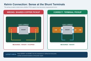
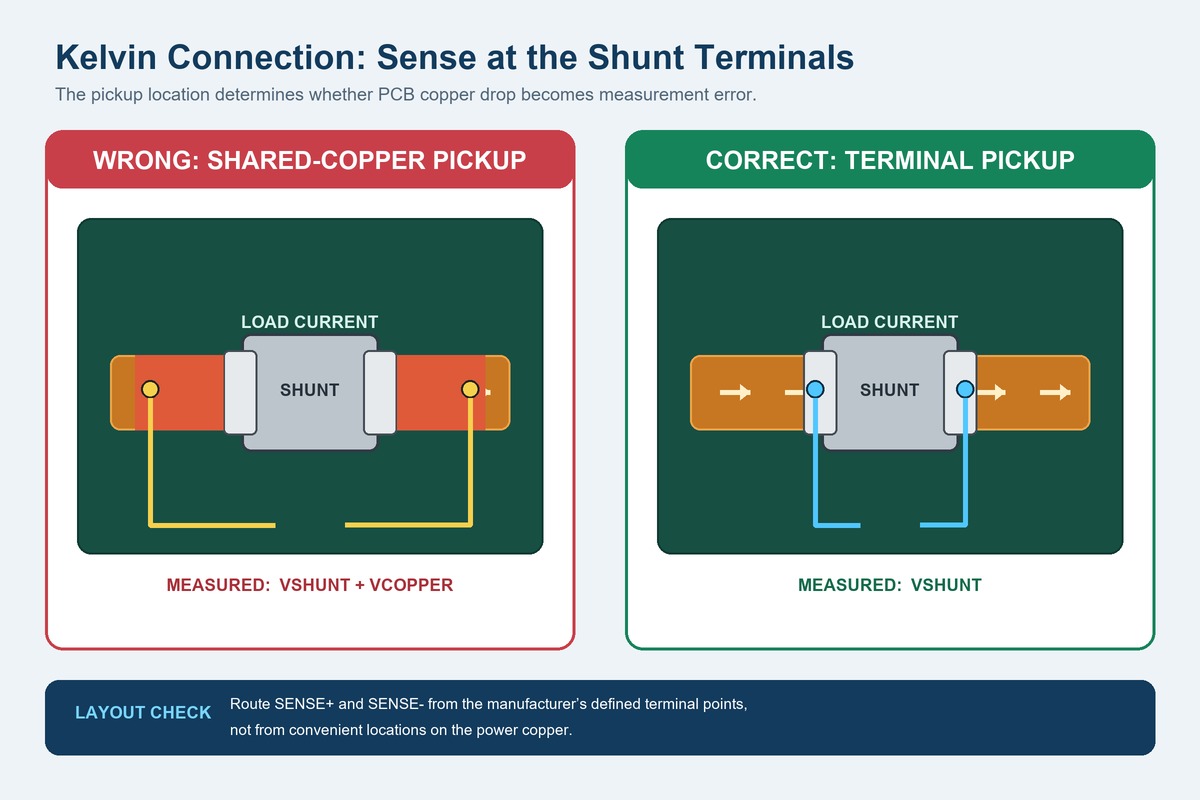
A Kelvin connection separates the voltage-sense path from the high-current path. The two sense traces begin at defined points on the resistor terminals, so voltage drop in the surrounding power copper, vias, pads, and high-current solder path is excluded from the measurement.

Review the layout in this order:

  • Avoid a narrow or asymmetric current entry. Prefer a short, balanced path into both shunt terminals, without unreviewed neck-downs or thermal reliefs.
  • Avoid taking SENSE+ and SENSE- from convenient points on a copper pour. Prefer connections at the terminal locations recommended by the shunt manufacturer.
  • Avoid separating the two sense traces or routing them beside switching nodes. Prefer a close, balanced pair kept away from gate-drive loops and inductors.
  • Avoid sharing sense or reference copper with load-current return. Prefer dedicated low-current paths from the shunt to the amplifier.

For a four-terminal shunt, keep current pads and sense pads distinct. For a two-terminal shunt, pad geometry and trace entry become even more important. A schematic net name does not prove that the physical connection is correct; the copper must be reviewed at the resistor terminals.

Place any approved input filter symmetrically and close to the amplifier. Keep test points on the same nodes used by the measurement circuit. If a fixture measures from different locations, it can pass a board that the product itself reads differently.

A Kelvin error often looks deceptively correct on one prototype. Calibration may remove the error at one current and temperature, but it cannot make changing copper drop disappear across load, temperature, and production variation. If the reading changes when the current path heats, inspect the physical sense-point location before changing calibration constants.

shunt resistor

What Can Distort Current Measurement After Assembly?

Assembly introduces variation that is absent from the schematic. Unequal solder volume can move the effective current-entry point. Poor wetting can increase local resistance. Mechanical stress and board flex can affect the resistor, while heat from nearby components can shift both the shunt and amplifier behavior.

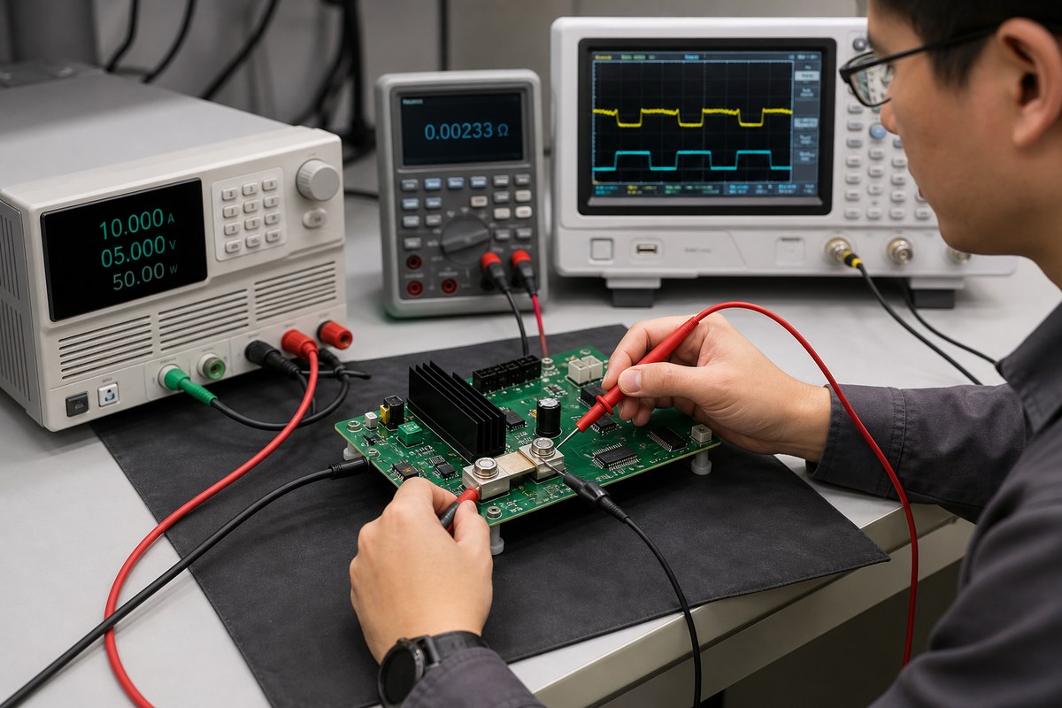
Visible inspection is necessary but not sufficient. AOI can verify component presence and visible solder condition; X-ray can help with hidden connections. Neither proves electrical accuracy. A useful test must specify current, measurement nodes, warm-up or dwell time, temperature condition, acceptance limits, and the result to record.

Use four controls with different purposes:

  • Incoming material — verify the approved manufacturer, part number, lot information, and any required traceability.
  • Assembly workmanship — inspect placement, solder wetting, bridging, contamination, damage, and component seating.
  • PCB implementation — confirm the released current path, Kelvin points, copper construction, and revision were actually built.
  • Electrical acceptance — apply customer-defined current points and verify the measured output, trip behavior, or calibration result within the approved limits.

Example production test plan

  • Test at 10%, 50%, and 100% of the approved operating current.
  • Use the same Kelvin nodes read by the product, not convenient fixture points elsewhere on the power copper.
  • At the high-current point, record the result after the defined warm-up or thermal-stabilization period.
  • Retain input current, shunt voltage, amplifier or ADC output, calculated error, and pass/fail result.

The exact current points and limits must come from the customer’s approved specification; the example shows the level of detail needed for a repeatable test.

Different symptoms suggest different checks: low-current instability calls for noise and offset review; high-current drift calls for thermal review; large board-to-board spread calls for BOM, solder, copper, and fixture comparison. This diagnostic order prevents repeated calibration from hiding a manufacturing problem.

A Shunt Resistor PCB Assembly Example

An ADC current-sensing PCBA project illustrates how an electrical requirement becomes a manufacturing package. The board used four-layer FR-4 with Tg150 material, 2 oz copper on the inner and outer layers, 1.6 mm thickness with ±10% tolerance, and lead-free HASL.

The customer first reviewed the production data and panelization files before fabrication. This created a clear release point: manufacturing preparation could proceed only after the customer confirmed that the production package still represented the intended board.

The SMT build also assigned clear responsibilities:

  • EBest sourced all components, keeping material responsibility with one assembly partner.
  • The boards were separated after SMT and delivered as individual units, so the required delivery format was defined before production.
  • Post-SMT cleaning required the boards to be free of solder balls and other contamination before shipment.

The customer value came from the sequence: define the board construction, approve the production interpretation, assign component responsibility, specify the delivery condition, and make cleanliness an acceptance requirement. Each control removed a different source of ambiguity before shipment.

For a similar project, add the electrical acceptance layer before quotation: the exact shunt part number, approved Kelvin nodes, operating and fault-current range, allowed error, test current points, warm-up condition, and required test record. That gives the manufacturer something objective to build and verify.

The project followed a practical handoff: the customer defined and approved the production interpretation; EBest controlled board construction, sourcing, SMT, separation, and cleanliness; electrical acceptance still required customer-approved current points and limits. That division gives both sides a clear decision before material purchase and a clear acceptance basis before shipment.

What Files Support a Shunt Resistor PCBA Review?

Send one revision-controlled package. At minimum, it should contain Gerber or ODB++ data, fabrication drawing, BOM, pick-and-place file, assembly drawing, and test specification. Mismatched revisions can invalidate an otherwise careful review.

Use each file to answer a specific production question:

  • Fabrication data — What stackup, copper weight, thickness, finish, current-path geometry, and critical dimensions must be built?
  • BOM — Which exact shunt, amplifier, filter components, and approved alternates may be purchased?
  • Assembly data — Where is each part placed, what workmanship or stencil notes apply, and which areas require special inspection?
  • Test specification — Which current is applied, where is voltage measured, how long must the board stabilize, what limits apply, and what evidence is retained?

Also state quantity, prototype or production stage, delivery format, traceability needs, and first-article requirements. For functional testing, provide the fixture interface, power sequence, firmware state, safe operating limits, calibration instructions, and pass/fail criteria.

EBest Circuit can review the manufacturing package, fabricate the PCB, support controlled component sourcing, assemble and inspect the board, and coordinate agreed testing. Circuit architecture, the accuracy budget, safety requirements, and final product validation remain customer-controlled decisions.

Shunt Resistor FAQs

What resistance value should a shunt resistor use?

Start with maximum current and permitted sense voltage, then verify continuous power, transient energy, temperature rise, amplifier range, and the full error budget. There is no universal best resistance value.

Why is a Kelvin connection important for a shunt resistor?

It prevents voltage drop in shared high-current copper and pad paths from being included in the sensed voltage. The smaller the shunt value and signal, the more important the physical sense-point location becomes.

Can a normal resistor replace a current-sense resistor?

Not without review. In a shunt resistor vs normal resistor comparison, nominal resistance alone is not enough. Tolerance, TCR, continuous and pulse ratings, terminal structure, package, land pattern, and thermal behavior must meet the approved requirements.

Can AOI verify shunt resistor accuracy?

No. AOI can verify visible assembly conditions and component presence. Accuracy requires an electrical test with defined current, nodes, temperature or warm-up condition, limits, and records.

What should be sent for a shunt resistor PCBA quotation?

Send controlled PCB data, fabrication drawing, BOM, pick-and-place file, assembly drawing, and test requirements. Include the current range, critical sense points, approved parts, quantity, delivery format, and required records.

Need a Shunt Resistor PCBA Review? Send your PCB data, fabrication drawing, BOM, assembly files, current range, and test requirements to sales@bestpcbs.com. EBest Circuit can review the manufacturing package and help align PCB fabrication, component sourcing, assembly, inspection, and agreed testing before quotation.

You may also like

Digital Potentiometer PCB Guide: Selection and PCBA Checks

August 18th, 2026

A digital potentiometer adjusts resistance through an electronic command instead of a mechanical knob. It is often used for calibration, gain control, sensor trimming, display adjustment, and other settings that need to be changed by a microcontroller.

Choosing one for a PCB involves more than selecting a resistance value. The device must work with the circuit voltage, provide the right resolution, behave correctly when power is turned on, and fit the approved PCB footprint. The assembled board also needs a functional test that confirms the output changes as intended.

This guide explains the information engineers and buyers should check when selecting a digital potentiometer and preparing a board for PCB assembly.

digital potentiometer
Digital potentiometer PCB integration for a compact mixed-signal control board.

What Is a Digital Potentiometer and How Does It Work?

A digital potentiometer, often called a digipot, contains a resistor string and an electronically controlled wiper. A microcontroller changes the wiper position through SPI, I2C, up/down pins, or, in some products, pushbuttons.

The high, low, and wiper terminals resemble the three terminals of a mechanical potentiometer, but they cannot always be used in the same way. They are semiconductor connections with limits on voltage, current, and power. Some devices allow signals only between their supply rails, while others support a wider terminal range. The exact datasheet must be checked before the part is placed in the circuit.

The main specifications include:

  • End-to-end resistance and tolerance
  • Number of taps and step size
  • Linear or logarithmic adjustment
  • Wiper resistance and current limit
  • SPI, I2C, or up/down control
  • Volatile or nonvolatile memory
  • Power-on wiper position
  • Package, pinout, and temperature grade

Use the complete manufacturer part number in the BOM. Parts in the same family may have different resistance values, memory options, interfaces, or packages, even when their abbreviated descriptions look similar.

Digital Potentiometer vs Analog Potentiometer for PCB Design

A mechanical potentiometer keeps its physical wiper position when power is removed. A digital potentiometer may return to a default value or recall a stored setting, depending on the device. This difference can affect how the product behaves during startup.

Design questionDigital potentiometerMechanical potentiometerWhat to check
How is it adjusted?Firmware or digital inputKnob, slider, or trimmerWho needs to change the setting?
What happens at power-up?Default or stored codeWiper stays in positionIs the initial output safe?
What signal can it handle?Limited by IC ratingsLimited by track and contact ratingsCheck actual voltage and current
How is it mounted?Small IC packageMechanical body and mounting hardwareCheck PCB and enclosure space
How is it tested?Send a command and measure the outputMove the wiper and measure the outputDefine the expected result

A digipot is useful when the setting must be controlled remotely, repeated accurately, saved in memory, or adjusted during automatic calibration. A mechanical potentiometer may be better when the circuit must work without power, the user needs direct manual control, or the signal exceeds the ratings of available digital devices.

How to Choose a Digital Variable Resistor

Start with the circuit rather than a distributor search filter. First determine the resistance range, required adjustment resolution, signal voltage, and current through the wiper. Then compare suitable parts using the manufacturer datasheets.

Tolerance deserves particular attention. A device marked 10 kΩ may not provide exactly 10 kΩ from end to end, and the wiper itself adds resistance. The load connected to the wiper can change the output again. If the circuit needs an accurate voltage or gain, calculate the expected range rather than relying only on the nominal resistance.

Also check what happens when the product is switched on. A volatile digipot normally starts at a defined default position and must be set by firmware. A nonvolatile version can recall a saved setting, but its memory has specified write and retention limits.

Before approving the part, confirm:

  • The terminal voltage remains within the datasheet limits during startup, normal use, shutdown, and faults
  • The wiper current and resistor power remain within their ratings
  • The controller supports the required interface and logic voltage
  • The number of taps provides enough adjustment resolution
  • The selected memory behavior suits the product
  • The exact package is available in both prototype and production quantities

These details are more useful in an RFQ than a description such as “10 kΩ digital potentiometer.”

How Does a Digital Potentiometer Circuit Connect to a PCB?

The digital interface and the analog signal path should be reviewed separately. A correct SPI or I2C response only shows that communication is working; it does not show that the analog output is correct.

For SPI, check the clock mode, chip-select timing, data order, maximum clock rate, and reset state. For I2C, check the device address, pull-up voltage, bus loading, and possible address conflicts. Up/down devices need defined direction and step timing.

On the analog side, follow the signal through the high, low, and wiper terminals. Make sure the schematic symbol matches the datasheet pin numbers and that the terminal voltage stays within the permitted range in every power condition. Unused address, reset, write-protect, or shutdown pins should not be left in an undefined state.

Place the recommended decoupling components close to the supply pins. If the wiper carries a sensitive analog signal, keep it away from noisy switching nodes where possible. Test points for the supply, control bus, and wiper output will make prototype debugging and production testing easier.

Digital Potentiometer IC Package and Footprint Checks

The footprint should be checked against the package drawing for the exact ordering code, not against a similar library part. Pay particular attention to whether the manufacturer drawing uses a top or bottom view and how Pin 1 is marked.

Compare the datasheet, schematic symbol, PCB footprint, BOM, pick-and-place data, and assembly drawing. They should agree on:

  • Package name, body size, pitch, and pin count
  • Pin numbering and Pin 1 orientation
  • Pad, solder-mask, and paste dimensions
  • Exposed-pad connection and paste pattern, if present
  • Component height and nearby clearance
  • Moisture sensitivity and storage requirements
digital potentiometer
Microscope inspection supports package-orientation and solder-joint checks during PCB assembly.

Small DFN and QFN packages need extra care because most solder joints are hidden under the component. AOI can confirm placement and visible features, but X-ray inspection may be needed to assess hidden joints or an exposed thermal pad. The inspection requirement should be agreed before assembly rather than added after a problem appears.

Digipot BOM, Sourcing, and Substitution Checks

The BOM should list the complete manufacturer part number, not only the resistance and package. It is also helpful to include the interface, number of channels, tap count, memory type, and temperature grade so that purchasing can distinguish between similar versions.

A proposed alternate should be checked for more than pin compatibility. Two parts can fit the same pads but use different commands, start at different wiper positions, or have different limits for terminal voltage and wiper current.

Check an alternate in four areas:

  1. Package: pinout, dimensions, height, and land pattern.
  2. Electrical performance: resistance, tolerance, wiper resistance, voltage, current, bandwidth, and temperature range.
  3. Digital operation: interface timing, address or command format, reset behavior, and memory operation.
  4. Supply status: source, traceability, lifecycle, moisture condition, lead time, and available quantity.

If the alternate requires a firmware change, the updated firmware version should be released with the BOM change. The contract manufacturer can provide sourcing information, but the design owner should approve the replacement before it is used.

Electronic Potentiometer PCBA Inspection and Testing

Assembly inspection and functional testing serve different purposes. AOI can detect many placement, polarity, marking, and visible solder defects. X-ray can provide information about joints hidden under the package. Neither test confirms that the digipot produces the correct analog output when it receives a command.

Possible problemUseful production evidenceInformation needed from the customer
Wrong part or suffixPackage marking and BOM checkApproved MPN and alternates
Wrong orientation or solderingFirst-article inspection, AOI, and X-ray where neededAssembly drawing and acceptance requirements
Wrong startup settingPower-cycle test and initial output measurementRequired startup value and timing
Incorrect adjustmentMinimum, midpoint, and maximum command testsCommands, test points, and output limits
Setting is not retainedWrite, power-off, restart, and readback testRequired memory behavior
digital potentiometer
Functional PCBA testing checks whether the commanded wiper settings produce the expected analog output.

A practical test instruction identifies the power supply, connection points, commands, expected outputs, tolerances, and records to keep. Testing three or more wiper positions is usually more informative than checking communication alone. The limits should come from the complete circuit because wiper resistance, loading, temperature, and surrounding components all affect the measured result.

A Digital Potentiometer PCBA Project Example

One customer’s project used a four-layer FR-4 PCB with a finished thickness of 1.6 mm, TG170 material, and 2 oz finished copper on the outer and inner layers. The board had an ENIG finish, blue solder mask, white silkscreen, and a minimum hole-copper requirement of 25 µm.

The customer reviewed the production data before fabrication. The bare PCBs received electrical testing, and the assembly requirements included SMT, AOI, X-ray, test images, board cleaning, individual-board delivery, and antistatic packaging.

The project record does not specify whether a digital potentiometer was fitted. For a digipot on this type of PCBA, the manufacturing package would also need:

  • The BOM and assembly drawing should show the complete part number, package, and Pin 1 orientation.
  • The inspection plan should state whether the package has hidden joints that require X-ray.
  • The functional test should send defined commands and measure the output at minimum, midpoint, and maximum settings.
  • If the setting must survive a power cycle, the test should verify that behavior as well.

These checks confirm three different things: the bare PCB has no opens or shorts, the component is assembled correctly, and the completed circuit responds correctly to the control commands. All three results matter when a digital potentiometer is part of the design.

FAQs About Digital Potentiometer PCB Integration

Can a digital potentiometer directly replace any analog potentiometer?

No. Compare terminal voltage, wiper current, resistance, power, bandwidth, adjustment law, startup state, control method, and package. A circuit that works with a mechanical potentiometer may exceed the limits of a digipot.

Should I choose SPI or I2C for a digital potentiometer?

Choose the interface that fits the controller, available pins, bus architecture, speed, addressing, and firmware. Then check logic levels, pull-ups or chip select, reset behavior, and what happens when one device is unpowered.

Why does the measured output differ from the ideal tap value?

End-to-end tolerance, wiper resistance, loading, temperature, and surrounding components all affect the result. Use a worst-case circuit calculation to set limits, then confirm them on representative assemblies.

What should a digital potentiometer PCBA RFQ include?

Provide the approved PCB fabrication data, BOM with full MPNs, pick-and-place data, assembly drawings, approved alternates, test points, firmware or command requirements, and measurable acceptance limits.

What can EBest Circuit verify?

EBest Circuit (Best Technology) can support component sourcing, DFM review, PCB fabrication, PCBA, inspection, and testing to the requirements supplied with the order. Circuit design, component approval, firmware, and product-specific acceptance limits should be provided or approved by the customer. Send your files to sales@bestpcbs.com for review.

You may also like

Standard Resistor Values: E-Series and BOM Checks

August 18th, 2026

This guide explains how standard resistor values work and how to turn a calculation into a controlled BOM decision. The goal is to reduce sourcing questions, unapproved substitutions, placement errors, and PCBA rework before files reach production.

standard resistor values
Standard resistor values support clearer selection before PCB assembly.

What Are Standard Resistor Values?

Standard resistor values are preferred nominal resistance values arranged in E-series. Instead of manufacturing every possible resistance, suppliers offer repeatable values across each decade, such as 10 Ω, 100 Ω, 1 kΩ, 10 kΩ, and 100 kΩ.

The number after E indicates how many nominal values appear in one decade. E12 contains 12 values, E24 contains 24, and E96 contains 96. A base value repeats by powers of ten, so 4.7 can represent 4.7 Ω, 47 Ω, 470 Ω, 4.7 kΩ, or 47 kΩ.

Before selecting a part, confirm:

  • The acceptable resistance window under worst-case operating conditions.
  • Tolerance and temperature coefficient, not only the nominal value.
  • Package, power rating, working voltage, pulse capability, and technology.
  • A manufacturer part number that is available for the intended production quantity.

A value being standard does not guarantee that every manufacturer offers it in every package or rating. The datasheet and orderable part number remain the final production reference.

Standard Resistor Values Table

The table below lists common base values within one decade. Multiply or divide them by powers of ten to reach the required range. For example, the E24 base value 24 can represent 2.4 Ω, 24 Ω, 240 Ω, 2.4 kΩ, or 24 kΩ.

SeriesValues per decadeCommon tolerance associationBase values
E6620%10, 15, 22, 33, 47, 68
E121210%10, 12, 15, 18, 22, 27, 33, 39, 47, 56, 68, 82
E24245%10, 11, 12, 13, 15, 16, 18, 20, 22, 24, 27, 30, 33, 36, 39, 43, 47, 51, 56, 62, 68, 75, 82, 91
E48482%Finer three-significant-digit spacing
E96961%Finer three-significant-digit spacing
E1921920.5% or tighterVerify the selected product family and datasheet

These tolerance relationships are common associations, not universal purchasing rules. For example, manufacturers also offer many E24 values with 1% tolerance. Always qualify the actual resistor family rather than inferring every specification from the E-series alone.

standard resistor values
Engineers compare E-series options, tolerance, and availability before releasing a resistor part.

E Series Resistors and Tolerance

A denser E-series provides more nominal values within each decade. It helps the selected resistance sit closer to the calculated target, but it does not prove that the full circuit will meet its error budget.

DecisionWhat can go wrongWhat to verify
Use a wider-tolerance partGain, bias, current, or threshold may move outside limits.Worst-case circuit result at both tolerance limits.
Choose a tighter E-seriesThe nominal value is closer, but drift or ratio error may still dominate.TCR, matching, long-term stability, and adjacent component tolerances.
Reduce BOM varietyA convenient common value may not meet the function.Whether the substituted value remains inside the approved electrical window.

For a pull-up or indicator circuit, an E12 or E24 value may provide enough margin. A precision divider, sensor interface, amplifier feedback path, or current-sense circuit may need an E96 value, tighter tolerance, lower TCR, or matched network. The customer engineering team owns the functional limits and released design; the assembly supplier should follow the approved BOM and substitution rules.

E24 Resistor Values for General PCB Assemblies

E24 resistor values offer 24 nominal choices per decade and are widely used where a 5% value provides sufficient circuit margin. The series adds intermediate options such as 11, 13, 16, 20, 24, 30, 36, 43, 51, 62, 75, and 91 that are not present in E12.

E24 is often practical when:

  • The function is tolerant of modest resistance variation.
  • The value is used for non-critical bias, indication, damping, or ordinary pull-up and pull-down duties.
  • Cost, availability, and lower BOM variety matter more than very fine nominal spacing.
  • Worst-case calculations confirm that the chosen value and tolerance are safe.

Do not use the application name alone to approve a resistor. A 330 Ω part may work for one LED circuit but overdrive or underdrive another because supply voltage, LED forward voltage, and target current differ. Calculate the function first, then select the E24 value that keeps the full operating range within limits.

E96 Resistor Values for Precision Circuits

E96 resistor values provide 96 nominal choices per decade and are commonly associated with 1% resistors. Their three-significant-digit spacing supports closer selection for analog feedback, sensing, precision division, filtering, and control functions.

E96 base values (100–976 within one decade)
100, 102, 105, 107, 110, 113, 115, 118, 121, 124, 127, 130
133, 137, 140, 143, 147, 150, 154, 158, 162, 165, 169, 174
178, 182, 187, 191, 196, 200, 205, 210, 215, 221, 226, 232
237, 243, 249, 255, 261, 267, 274, 280, 287, 294, 301, 309
316, 324, 332, 340, 348, 357, 365, 374, 383, 392, 402, 412
422, 432, 442, 453, 464, 475, 487, 499, 511, 523, 536, 549
562, 576, 590, 604, 619, 634, 649, 665, 681, 698, 715, 732
750, 768, 787, 806, 825, 845, 866, 887, 909, 931, 953, 976

Move the decimal point to reach the required decade: 487 can represent 48.7 Ω, 487 Ω, 4.87 kΩ, or 48.7 kΩ. Before releasing an E96 part, confirm whether absolute tolerance, resistor ratio, TCR, thermal gradients, noise, or long-term drift controls the real accuracy.

A tighter nominal value can also increase sourcing constraints. When alternates are allowed, define the acceptable resistance, tolerance, TCR, package, power, voltage, technology, and qualification requirements rather than approving ‘same value’ substitutions.

How to Find the Nearest Standard Resistor Value

The nearest numerical value is not automatically the safest production choice. The correct direction depends on what failure must be prevented. A higher resistance may reduce LED current, but it may also slow a pull-up edge or change amplifier gain.

Use this selection sequence:

  1. Calculate the ideal resistance using worst-case supply, load, temperature, and component limits.
  2. Define the minimum and maximum resistance that keep the circuit inside its approved operating window.
  3. Select the appropriate E-series and identify the nearest lower and higher standard values.
  4. Apply resistor tolerance to both candidates and repeat the worst-case calculation.
  5. Verify power dissipation, derating, working voltage, pulse energy, TCR, package, footprint, and availability.
  6. Release one exact manufacturer part number and document the approved alternate criteria.

Example: an LED calculation produces 193 Ω. Possible preferred values include 180 Ω and 200 Ω in E24, or 191 Ω and 196 Ω in E96. If excess current is the main risk, the higher value may provide more margin, but brightness and minimum-current requirements must still be checked. The calculation, not the lookup table, approves the part.

Standard SMD Resistor Values for PCBA

Standard SMD resistor values follow the same preferred E-series used by through-hole resistors. Package size changes assembly and electrical limits; it does not create a separate nominal-value system.

A BOM line that says only ’10 kΩ resistor’ leaves too many production decisions unresolved. A sourcing team may find many 10 kΩ parts with different tolerance, size, power, working voltage, TCR, pulse rating, construction, termination, lifecycle status, and price.

A production-ready resistor BOM line should confirm:

  • Nominal resistance with an unambiguous unit, such as 4.7 kΩ rather than 4.7.
  • Tolerance, package, power rating, and maximum working voltage.
  • TCR, pulse capability, current-sense construction, or other function-specific limits when relevant.
  • Manufacturer name, exact manufacturer part number, and lifecycle status.
  • Approved alternates or a clear no-substitution instruction.

  • Footprint, pick-and-place data, polarity rules where applicable, and assembly drawing consistency.

Very small SMD resistors may have no readable top marking. Reel labels, incoming inspection, feeder setup, material traceability, automated optical inspection, and electrical test requirements therefore matter more than visual identification alone.

standard resistor values
BOM, reel, footprint, and inspection checks help prevent wrong-value SMD resistor substitutions.

EBest Circuit (Best Technology) can support PCB fabrication, BOM and component sourcing review, SMT or through-hole assembly, inspection, and agreed testing coordination within the released project scope. The customer retains responsibility for circuit function, tolerance limits, approved substitutions, firmware, certification, and final product validation.
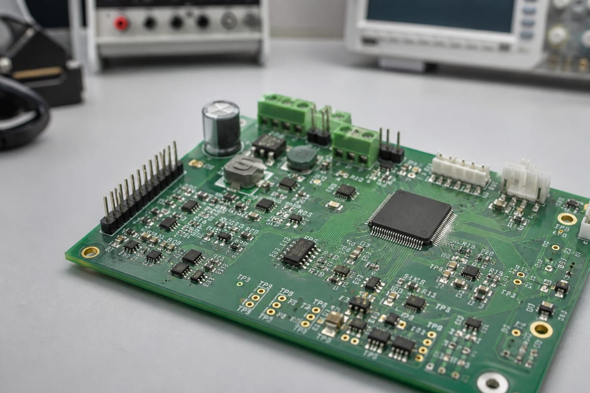
FAQ About Standard Resistor Values

1. What are the most common standard resistor values?

Common examples include 10 Ω, 22 Ω, 47 Ω, 100 Ω, 220 Ω, 330 Ω, 470 Ω, 1 kΩ, 2.2 kΩ, 4.7 kΩ, 10 kΩ, 47 kΩ, and 100 kΩ. Their popularity does not make them correct for every circuit.

2. What is the difference between E12, E24, and E96?

E12 has 12 nominal values per decade, E24 has 24, and E96 has 96. A denser series gives more choices, but tolerance, TCR, power, voltage, package, and availability still need separate confirmation.

3. Are 1% resistors always E96 values?
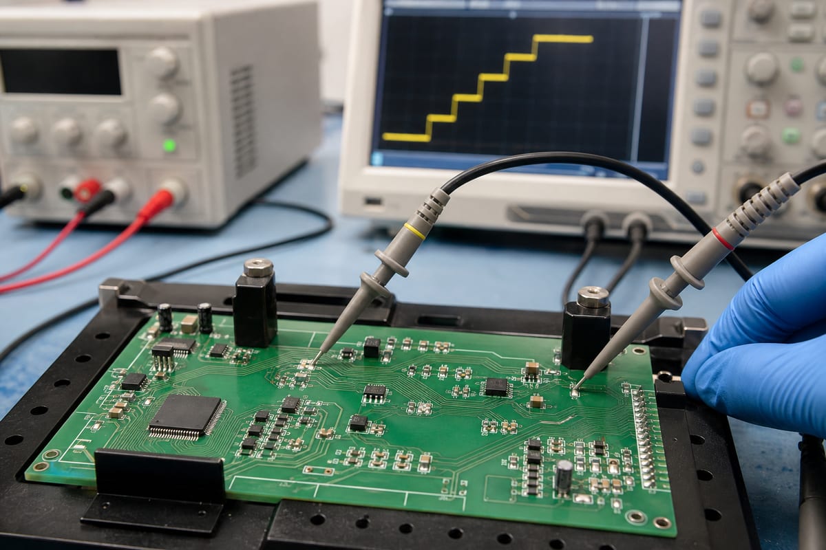
No. E96 is commonly associated with 1% tolerance, but tolerance and nominal-value series are separate specifications. Many E24 values are also available as 1% parts.

4. Can I always choose the nearest standard resistor value?

No. Compare both the lower and higher candidates under worst-case circuit conditions. The safe direction depends on whether the function controls current, gain, timing, bias, threshold, damping, or another parameter.

5. Are standard SMD resistor values different from through-hole values?

They use the same preferred-value concept. The available resistance range and electrical limits vary by package, resistor technology, tolerance, power, voltage, and manufacturer.

Ready to move your resistor-controlled PCB assembly into production? Send your Gerber files, controlled BOM, pick-and-place data, assembly drawings, quantity, approved substitution rules, and test requirements to sales@bestpcbs.com. EBest Circuit (Best Technology) will review the package for PCB fabrication and PCBA quotation, helping you identify unclear resistor specifications before sourcing and assembly.

You may also like

LED Symbol in Circuit: Polarity, Diagrams and PCB Design

August 17th, 2026

The led symbol identifies a light-emitting diode in a schematic, but reading it correctly requires more than recognizing the two outward arrows. A usable design must also preserve anode and cathode orientation, select a suitable current-control method, map the schematic pins to the correct PCB footprint, and communicate polarity clearly to assembly and inspection teams.

LED symbol in circuit with PCB and polarity design

What Is an LED Symbol?

An LED symbol is the schematic representation of a light-emitting diode. Its diode element indicates a polarized semiconductor junction, while two arrows pointing away from the device indicate emitted light. The bar side marks the cathode in the schematic; the opposite terminal is the anode. Designers commonly assign the reference designator D, such as D1 or D12, although some libraries use LED-specific prefixes.

The symbol is only one part of the component definition. A complete CAD record should also include the manufacturer part number, electrical model, package, pin numbers, PCB land pattern and assembly data. If the schematic symbol has anode on pin 1 but the footprint maps pin 1 to the physical cathode pad, the drawing can look correct while the assembled board is wrong.

What Do the Arrows on an LED Symbol Mean?

The two arrows show that the device converts electrical energy into emitted light. Their direction distinguishes the LED from a photodiode: LED arrows point outward, while photodiode arrows point toward the junction because a photodiode receives light. A standard rectifier or signal diode has no light arrows.

LED symbol compared with diode and photodiode symbols

Arrow direction describes optical function, not current direction. Conventional forward current enters the anode and leaves the cathode. The cathode bar remains the reliable schematic cue when the arrows are small or when a dense drawing is viewed at reduced scale.

How Does an LED Work in a Circuit?

An LED emits light when it is forward biased and current passes through its semiconductor junction. The supply must raise the anode above the cathode by approximately the device’s forward voltage, VF. Forward voltage varies with semiconductor material, color, current and junction temperature, so a nominal value from a generic chart is not a substitute for the selected LED datasheet.

A resistor, constant-current driver or regulated switching stage must control current. Connecting a bare LED directly across a stiff voltage source can produce thermal runaway or immediate overcurrent damage. For PWM dimming, verify peak current, duty cycle, driver timing and the LED’s pulsed-current limits rather than assuming that a low average current makes every pulse safe.

How Do You Identify LED Symbol Polarity?

In the schematic, the cathode is the terminal at the bar and the anode is the opposite terminal. On a common through-hole LED, the longer lead is often the anode and a flat on the body often indicates the cathode. These physical cues are useful during prototyping, but leads may be trimmed and package conventions can vary.

LED symbol polarity with anode cathode through-hole and SMD identification

SMD LED polarity marks are package-specific. A notch, chamfer, colored stripe, internal electrode shape or printed mark may identify one terminal, but the same-looking mark is not guaranteed to mean the same thing across suppliers. Confirm the polarity diagram and recommended land pattern in the exact manufacturer datasheet, then make the schematic pin numbers, footprint pad numbers, silkscreen and pick-and-place rotation agree.

How Is an LED Symbol Used in a Circuit Diagram?

The led symbol circuit connection should make four relationships unambiguous: the drive source, the current-control element, the return path and the polarity. A simple indicator may place the LED and resistor between a logic output and ground. A low-side transistor driver places the LED load toward the supply and switches the return path. A high-side driver reverses that arrangement. In each case, the symbol orientation must reflect the intended conventional current path.

Net labels should identify important rails and control signals, while reference designators allow the BOM, placement file and test procedure to refer to the same component. When several colors or status channels are present, include color or function in the schematic notes, such as STATUS_GREEN or FAULT_RED, rather than expecting assembly staff to infer function from the symbol.

What Is the Difference Between an LED, Diode and Photodiode Symbol?

Device Symbol cue Primary circuit role Design detail to verify
Standard diode Diode element without light arrows Rectification, clamping or switching Forward current, reverse voltage and recovery behavior
LED Two arrows pointing outward Light emission, indication or illumination Forward voltage, current, color, optical output and thermal limit
Photodiode Two arrows pointing inward Optical sensing Bias mode, dark current, spectral response and amplifier interface

A schematic library should not reuse one symbol interchangeably for all three devices. Even when the footprint is similar, their electrical limits, test conditions and functional intent differ. Clear symbols also reduce review errors when a design contains emitters and optical receivers in the same circuit.

What Do Single-Color, Bicolor and RGB LED Symbols Show?

A single-color LED normally has one junction and two pins. A two-lead bicolor LED can contain two dies connected in inverse parallel; reversing current changes the active color. A three-lead bicolor device may use a common anode or common cathode. RGB LEDs commonly have four leads for red, green and blue channels plus a shared terminal, although addressable RGB packages may integrate a controller and use power, ground and data pins instead.

The schematic must show the actual internal connection. A generic three-diode drawing cannot tell assembly or firmware teams whether the package is common-anode, common-cathode or independently connected. Use the selected part’s pin numbering, give each color channel its own current-control element when required, and verify that the PCB footprint orientation matches the datasheet top-view or bottom-view convention.

What Information Does the LED Symbol Not Show?

The graphic does not specify forward voltage, rated current, luminous intensity, wavelength, viewing angle, reverse-voltage limit, ESD sensitivity, package dimensions or thermal resistance. It also does not establish whether the component is suitable for reflow, wave soldering, hand soldering or a particular cleaning process.

The BOM and datasheet must carry those requirements. For color-critical products, define wavelength or chromaticity and binning rather than using only “red” or “white.” For brightness matching, state the relevant optical bin and test current. For power LEDs, include the thermal-pad connection and maximum junction-temperature calculation. The symbol communicates connectivity; it does not replace component qualification.

How Do You Calculate an LED Current-Limiting Resistor?

For a simple DC circuit, calculate the series resistor with R = (VS – VF) / IF. If a 5 V rail drives an LED with a 2.0 V forward voltage at 10 mA, the calculated resistance is 300 ohms. Selecting the next higher standard value, such as 330 ohms, reduces current slightly and provides margin for supply and forward-voltage tolerance.

LED symbol circuit with current limiting resistor formula

Check resistor dissipation with P = I2R and apply a sensible derating margin. Calculate worst cases using maximum supply voltage and minimum LED forward voltage for peak current, then minimum supply voltage and maximum forward voltage for minimum brightness. Separate current control is normally preferred for parallel LED branches because normal VF variation can make one branch take disproportionate current.

How Should an LED Footprint and Polarity Mark Be Designed on a PCB?

Start with the manufacturer-recommended land pattern, then check courtyard, solder-mask expansion, paste apertures and component-to-component spacing against the assembly process. Map anode and cathode pin numbers explicitly between the schematic and footprint. A pin-1 convention is useful only when it agrees with the package drawing and does not conceal the electrical polarity.

Place a visible cathode or anode cue on the silkscreen without printing over exposed copper or solderable pads. If board density removes the silkscreen mark, preserve polarity in the assembly drawing and fabrication documentation. The silkscreen PCB design guide explains practical text and clearance controls. For low-power indicators and control panels, a conventional FR4 printed circuit board is usually appropriate. The footprint still needs enough thermal relief for solderability and enough copper to support the expected current.

How Are SMD and Through-Hole LEDs Assembled?

SMD LEDs are placed from centroid data and package rotation, then reflowed according to the component’s moisture sensitivity, peak-temperature and time-above-liquidus limits. Through-hole LEDs require controlled insertion height, lead forming, polarity checks and either selective, wave or hand soldering. A spacer or mechanical fixture may be needed when optical alignment to a light pipe or panel opening matters.

AOI can verify component presence, orientation marks and visible solder joints, but optical inspection alone does not prove color, brightness or electrical function. Hidden thermal pads may justify X-ray, while a functional test should energize channels at controlled current and confirm the intended color and response. EBest Circuit (Best Technology) supports SMT, THT and mixed assembly, with components down to 01005 where the design and process allow; inspection can combine 3D SPI, AOI, X-ray and functional testing according to the actual risk.

For production that needs component sourcing, placement and test under one controlled workflow, the PCB assembly service covers both fabrication and assembly coordination. The BOM should identify the approved LED manufacturer part number, package, color/bin requirements and permitted substitutes so that a visually similar but electrically different LED is not installed.

What Causes an LED Circuit to Fail?

  • Reverse installation: schematic-to-footprint mapping, pick-and-place rotation or manual insertion places the cathode on the anode pad.
  • Excess current: the resistor or driver was selected from typical values without worst-case supply, temperature and forward-voltage limits.
  • Poor thermal path: a power LED’s thermal pad, copper area, dielectric and heat-sink interface cannot keep junction temperature within limit.
  • Inadequate ESD control: handling or test equipment damages the junction before final functional test.
  • Solder defects: insufficient paste, tombstoning, voiding, cold joints or excessive reflow exposure reduces electrical or thermal reliability.
  • Uncontrolled substitution: a replacement part has different polarity marking, pinout, optical bin or footprint dimensions.

Power LEDs need a board selected for the complete thermal path, not just the substrate name. A metal-core PCB can shorten the path from LED pad to heat sink; EBest Circuit (Best Technology) lists MCPCB thermal conductivity from 0.8 to 3.0 W/mK, subject to stack-up and engineering confirmation. For higher insulation or power-density requirements, a high-power LED ceramic PCB may provide a different thermal and dielectric balance.

LED PCB materials including FR4 metal core and ceramic boards

Where Are LEDs Used on PCBs?

Low-current LEDs provide power, status, fault and communication indicators. Backlight and user-interface boards distribute many LEDs behind light guides or diffusers. Industrial controls use optically visible state confirmation, while sensing systems combine emitters with photodiodes or phototransistors. Automotive, medical and instrumentation products may require controlled color, luminance uniformity, lifetime and environmental validation.

High-power lighting, UV curing, infrared illumination and machine vision place greater demands on current regulation and heat extraction. In these products, the led symbol remains simple, but the board may require an MCPCB, ceramic substrate, thermal vias, direct thermal pads or a mechanically controlled heat-sink interface. Material selection should follow the allowed junction temperature, dissipated power, electrical isolation and assembly process.

FAQ About LED Symbols

Which side of the LED symbol is positive?

The anode is the positive side during normal forward operation. The cathode is the side at the bar in the schematic. Always confirm the physical package mark and pin numbering in the selected component datasheet.

Does the LED symbol show the color?

No. Color may be added as a schematic note or component value, but the symbol itself does not guarantee wavelength or optical bin. Those details belong in the BOM and approved part specification.

Can an LED be connected without a resistor?

Only when another circuit element safely regulates current, such as a constant-current LED driver or a source with an intentionally limited output. A bare LED should not be connected directly across a low-impedance voltage rail.

Is an SMD LED polarity mark universal?

No. Package marks differ among manufacturers and package families. Use the exact datasheet polarity and land-pattern drawing rather than relying on a remembered stripe or notch convention.

Why does an LED work in the prototype but fail after assembly?

Common causes include reversed footprint mapping, pick-and-place rotation, substitute-part pinout differences, reflow damage, ESD, solder defects and insufficient thermal dissipation. Compare the schematic, footprint, BOM, placement file and assembly drawing as one linked data set.

Conclusion

Reading an LED schematic is straightforward once the outward light arrows and cathode bar are recognized, but a reliable board also needs correct pin mapping, controlled current, clear polarity marking, a validated footprint and suitable thermal construction. Treat the symbol, datasheet, BOM, placement data and PCB documentation as one consistent definition.

EBest Circuit (Best Technology) can support FR4, metal-core, ceramic PCB and complete PCBA requirements for LED products. For engineering review or a manufacturing assessment, contact sales@bestpcbs.com.

You may also like

TNC vs BNC: Which RF Connector Fits Your PCB?

August 17th, 2026

This guide compares tnc vs bnc from the buyer’s point of view, then translates the connector decision into the files, checks, and responsibilities needed for PCB fabrication and assembly. EBest Circuit (Best Technology) can support manufacturability review, PCB production, component sourcing, PCBA, inspection, and agreed testing coordination. Your engineering team remains responsible for RF architecture, operating targets, antenna and cable selection, environmental requirements, and final product validation.

tnc vs bnc
BNC uses bayonet coupling, while TNC uses threaded coupling.

What Is the Difference Between a BNC and a TNC Connector?

A BNC connector uses a bayonet-style coupling that mates with a push-and-turn action. A TNC connector uses a threaded coupling. That mechanical difference affects connection speed, resistance to unintended loosening, and how much clearance the installed connector needs.

The two connector families may look related, but a standard BNC and a standard TNC do not mate directly. An adapter can bridge selected interfaces, yet it adds another mechanical joint and RF discontinuity that the customer must include in the system review.

The practical choice usually starts with:

  • Connection frequency: how often operators must connect and disconnect the cable.
  • Mechanical environment: whether vibration, cable pull, or repeated handling can loosen the interface.
  • Approved RF requirements: the impedance, operating band, power, loss, and shielding targets defined by the system designer.
  • PCB and enclosure constraints: the footprint, board-edge position, connector height, wrench or hand clearance, and mating-cable path.

Do not choose only from a family name. Confirm the exact manufacturer part number and datasheet because frequency capability, impedance options, materials, sealing, mounting style, and termination details vary within both families.

TNC vs BNC Connector Specs That Affect Selection

Connector specifications matter only when they are tied to the released product conditions. A catalog maximum does not prove that a particular board launch, cable assembly, adapter, and enclosure will meet the customer’s complete RF target.

Decision factorBNCTNC
CouplingBayonet; quick connect.Threaded; secure connection.
Best fitBench use and frequent changes.Vibration and outdoor use.
Typical frequencyMany standard parts: about 4 GHz.Many standard parts: about 11 GHz.
InstallationAllow turning and cable clearance.Allow thread and tool clearance.
Release checkConfirm MPN, impedance, and footprint.Confirm MPN, impedance, and footprint.

Selection takeaway: the often-quoted 4 GHz for BNC and 11 GHz for TNC are useful family-level rules of thumb, not guaranteed limits for every connector. Ratings overlap, and some precision variants extend beyond them. Ask for the approved connector datasheet and a signal-path requirement. The exact board connector, cable connector, coax, adapter, and mating interface must be reviewed together.

TNC or BNC for Vibration and Outdoor Use?

A connector that loosens in service can produce intermittent faults that are difficult to reproduce during bench testing. Threaded TNC coupling is generally preferred when the product faces sustained vibration, vehicle movement, outdoor exposure, or cable loads. BNC remains practical where rapid connection changes matter and the installed environment is controlled.

Typical BNC applications include oscilloscopes, RF test instruments, patch panels, broadcast/video equipment, and radio or scanner ports that are connected and disconnected regularly. Typical TNC applications include GNSS/GPS receivers, vehicle and fleet radios, outdoor wireless equipment, industrial telemetry, and antenna feeds exposed to vibration or weather. These are application patterns, not automatic approval for a specific part.

Before choosing for a harsh environment, confirm:

  • Vibration and shock profile, including cable mass and the direction of cable pull.
  • Ingress, corrosion, temperature, and sealing requirements for the exact connector variant.
  • Whether the connector is panel-mounted, cable-mounted, or supported directly by the PCB.
  • Whether an enclosure, bracket, strain relief, or locking feature carries the mechanical load.
  • The inspection and acceptance method for thread engagement, bayonet locking, torque, or retention.

The PCB supplier should not infer these environmental requirements. The customer should release them with the approved connector and mechanical stack. EBest Circuit can then review manufacturability, connector placement, solder accessibility, and inspection points within the agreed build scope.

TNC vs BNC Cable and Antenna Interfaces

A correct board connector can still fail the project if the mating cable or antenna interface is wrong. BNC and TNC do not each belong to one coax type: both families are available for multiple cables. Compatibility depends on the exact connector’s supported cable dimensions, dielectric, shield construction, impedance, and termination method.

Common 50-ohm coax pairings include:

  • RG-174, RG-188, and RG-316: thin, flexible jumpers used inside equipment and in short RF or GNSS leads. Actual BNC and TNC product lines are available for these cables.
  • RG-58: a common general-purpose cable for test, radio, industrial, and antenna connections; the connector must match its exact cable construction.
  • RG-223 and RG-400: selected when improved shielding, temperature capability, or a more robust assembly is needed.
  • LMR-195 and LMR-240: often used for lower-loss antenna feeds; TNC is common, while compatible BNC parts also exist for selected constructions.
  • LMR-400 and other larger low-loss cables: used for longer outdoor antenna runs when loss matters, but require a connector specifically designed for the cable diameter and preparation dimensions.

For 75-ohm video systems, BNC is also widely paired with cables such as RG-59 and RG-6. Do not mix a 75-ohm cable/connector path with a 50-ohm RF design merely because the connectors can appear similar.

How BNC and TNC relate to antenna types:

  • Rubber-duck, short-whip, and so-called ‘chili pepper’ antennas may be supplied with BNC or TNC when they mount directly to a radio, receiver, or external port. BNC favors quick removal; TNC favors threaded retention.
  • External GNSS/GPS, vehicle, magnetic-mount, and outdoor antennas commonly use a coax lead terminated in TNC, although BNC, SMA, N-Type, and other options also exist.
  • A bare ceramic patch antenna is normally mounted on the PCB or connected by a short micro-coax lead, not directly by BNC or TNC. A finished active GPS antenna containing a ceramic element may use TNC or BNC at the end of its external cable.
  • An internal FPC antenna normally uses U.FL, I-PEX/MHF, another micro-coax connector, or a soldered feed. It reaches an external BNC or TNC port only through an approved pigtail, bulkhead cable, or adapter.

Treat the complete RF path as one controlled set:

  • PCB connector manufacturer and exact part number.
  • Mating cable connector, gender, standard or reverse polarity, and impedance.
  • Coax type, length, attenuation, power rating, bend radius, routing, and strain relief.
  • Antenna frequency bands, feed impedance, mounting method, and approved adapter if any.
  • Customer-defined insertion-loss, return-loss/VSWR, retention, and environmental acceptance limits.

The cable name alone is not an approval. Confirm the connector datasheet field commonly labeled ‘Cable Type’ or ‘Terminates To,’ then validate the assembled path. If an adapter is unavoidable, record it in the controlled BOM or interface drawing and include it in prototype validation rather than adding it informally at final assembly.

tnc vs bnc
Cable and antenna interfaces must match the approved connector and RF path.

TNC vs BNC Connector Footprint and Assembly Checks

Footprint errors are expensive because many RF connectors combine electrical pads, ground tabs, mounting posts, board-edge geometry, and enclosure alignment. A visually similar substitute may have different hole sizes, pin spacing, reference-plane needs, or body dimensions.

Release these checks before PCB fabrication:

  • Exact MPN and current manufacturer datasheet; do not release only ‘BNC’ or ‘TNC’ in the BOM.
  • Verified land pattern, drill sizes, plated-hole requirements, pad dimensions, and solder-mask clearances.
  • Connector datum, orientation, board-edge setback, body overhang, keepout, and mating direction.
  • Ground connection strategy and controlled RF geometry supplied by the customer’s RF designer.
  • Enclosure cutout, panel thickness, nut/washer stack, finger or wrench access, and cable bend clearance.
  • Assembly method, soldering access, thermal-mass concerns, support fixtures, and inspection criteria.

EBest Circuit can compare the released fabrication and assembly data for obvious manufacturability conflicts and coordinate sourcing against the approved BOM. The customer must approve the footprint, RF geometry, substitute part, and final mechanical interface before production release.

A TNC vs BNC PCB Assembly Example

A German industrial-vehicle customer needed a compact 2.4 GHz telemetry gateway for fleet equipment. Because its external antenna would face continuous vibration and outdoor service, the design used a 50-ohm panel-mount TNC connector with a sealed short-whip antenna. The threaded coupling offered more secure retention than a quick-release BNC interface.

Key PCB requirements:

  • 8-layer, 0.97 mm, 170 Tg FR-4 HDI with 0.5 oz copper.
  • L1-L2, L2-L7, and L7-L8 blind/buried vias; 0.10 mm minimum holes.
  • Resin-filled, planarized via-in-pad in the BGA area; black solder mask, white legend, and ENIG 1 microinch.
  • A 4.8 mil L1 trace referenced to L2 for the 50-ohm RF path, plus separate 90-ohm and 100-ohm differential structures with an impedance report.
  • Three panel-edge fiducials for SMT alignment.

Because the PCB was only 0.97 mm thick, the TNC was mounted to the enclosure instead of loading the board directly. A short RG-316 50-ohm pigtail connected the bulkhead TNC to the PCB RF interface, transferring vibration and cable pull to the enclosure.

Project plan:

  • 20 engineering units for fit, antenna matching, vibration, and functional checks.
  • 200 pilot units, followed by a planned 2,000-unit production lot after approval.
  • 15 business days for HDI PCB fabrication and 7 business days for PCBA after complete file and component release.
  • Inspection covered TNC engagement, bulkhead hardware, pigtail strain relief, continuity, and customer-defined 2.4 GHz acceptance limits.

This made the connector decision production-ready: threaded TNC retention outside the enclosure, flexible RG-316 routing inside, a verified 50-ohm PCB path, and documented impedance and assembly evidence.

tnc vs bnc
A panel-mounted TNC and RG-316 pigtail can keep cable load off a thin HDI PCB.

What to Include in a TNC or BNC RFQ

An RFQ should let the manufacturer quote the released board and connector interface without guessing. Missing part numbers, footprints, mechanical constraints, or test limits can produce a quick price that later changes after engineering review.

Include the following RFQ package:

  • PCB fabrication files, stackup requirements, controlled-impedance information, and fabrication drawing.
  • Assembly drawings, pick-and-place data, approved BOM, exact connector MPN, and approved alternates if any.
  • Connector and mating-interface datasheets, including gender, polarity, impedance, and mounting style.
  • Mechanical drawing or 3D data showing board edge, enclosure cutout, panel stack, cable route, and access clearance.
  • Prototype quantity, production forecast, packaging expectations, and connector handling requirements.
  • Customer-owned inspection and test limits, required records, sample size, and acceptance authority.

For a useful quotation, also state which decisions are frozen and which remain open. EBest Circuit can review the package for PCB/PCBA manufacturability and identify missing production inputs, but the customer must approve RF performance, interface compatibility, environmental compliance, and final acceptance criteria.

TNC vs BNC FAQs

Are BNC and TNC connectors interchangeable?

No. Standard BNC and TNC connectors use different coupling mechanisms and do not mate directly. Use only an approved adapter or matching cable interface, and include that added connection in mechanical and RF validation.

Is TNC always better than BNC?

No. TNC can provide a more secure threaded connection, while BNC offers faster bayonet coupling. The better choice depends on the exact part, operating band, handling frequency, vibration, environment, cable, enclosure, and system requirements.

Can a BNC PCB footprint be reused for a TNC connector?

Do not assume so. Compare the exact manufacturer drawings, pins, mounting posts, hole sizes, pad geometry, body envelope, board-edge datum, and mating direction. Release a verified footprint for the approved MPN.

Should a TNC-to-BNC adapter be used in production?

Only when the engineering team approves it as part of the controlled interface. The adapter adds length, a mechanical joint, and RF effects that must be included in clearance, retention, and performance validation.

What can EBest Circuit check before production?

EBest Circuit can support PCB/PCBA manufacturability review, BOM and sourcing coordination, fabrication, assembly, connector-placement and solder-joint inspection, and agreed test coordination. The customer owns RF design, connector selection, environmental requirements, released files, and final validation.

For a tnc vs bnc project, send your released PCB files, BOM, connector datasheets, mechanical interface drawing, and test requirements to sales@bestpcbs.com for a manufacturability and quotation review.

You may also like

Inductor Symbol Guide: Types, Meanings and Circuit Use

August 17th, 2026

An inductor symbol represents a component that stores energy in a magnetic field and opposes rapid changes in current. The familiar coil drawing identifies the component class, while added lines, arrows, taps and dots indicate its core, adjustability or magnetic coupling. Reading the drawing correctly is only the first step: a working PCB also needs the right inductance, current rating, DC resistance, self-resonant frequency, package and land pattern.

Inductor Symbol Guide: Types, Meanings and Circuit Use

What Is an Inductor Symbol?

The basic electrical inductor symbol is a series of curved loops between two terminals. It represents a conductive winding, not the exact number of turns or the component’s physical shape. A schematic may draw the loops horizontally or vertically without changing the electrical meaning. The reference designator normally starts with L, such as L1 or L203, and the inductance value is stated in henries, usually microhenries (uH) or nanohenries (nH) on PCB designs.

The symbol belongs to the logical schematic. It does not define whether the real component is a molded SMD power inductor, a small RF chip inductor, a common through-hole choke or a toroid. That physical decision is carried by the manufacturer part number, schematic properties, BOM and PCB footprint. A correct design keeps those records linked so that L1 cannot be assigned a symbol for one function and a land pattern for an incompatible package.

Why Is Inductance Represented by L?

Electrical schematics conventionally use L as the quantity and reference letter for inductance. The SI unit is the henry, written H. A value marked 10 uH beside L1 therefore means that the component’s nominal inductance is 10 microhenries; it does not describe its current capacity or resistance.

The voltage-current relationship is v = L di/dt. A larger inductance produces a larger voltage for the same rate of current change. Stored magnetic energy is W = 1/2 L I². These relationships explain why inductors smooth current in converters and filters, and why an interrupted inductive current can generate a large voltage transient. Real components also contain winding resistance, parasitic capacitance and core loss, so the ideal formula must be combined with datasheet limits.

How Does an Inductor Work in a Circuit?

Current through the winding creates magnetic flux. When the current changes, the changing flux induces a voltage that opposes that change. Under steady DC conditions, an ideal inductor eventually behaves like a short circuit. A real inductor retains its DC resistance and may heat from copper and core losses. At increasing frequency, inductive reactance rises according to XL = 2 pi fL until parasitic capacitance becomes significant near the self-resonant frequency.

In a buck converter, the inductor receives pulsed energy from the switching node and delivers a smoother current to the output. In an LC filter, it impedes high-frequency current while the capacitor diverts unwanted energy. In an RF matching network, a few nanohenries can tune impedance, but the pad geometry and nearby copper can contribute enough parasitic inductance and capacitance to alter the intended value.

Inductor symbol circuit examples in a buck converter and LC filter

What Are the Main Inductor Symbols?

Most inductor symbols begin with the same coil form. Additional marks tell the reader what magnetic structure or electrical behavior matters in that circuit. The exact graphic style can vary between IEC, ANSI/IEEE and CAD libraries, so a project’s symbol legend and component properties remain authoritative.

Symbol type Typical graphic feature What it communicates
Fixed or air-core inductor Coil with no parallel core lines Fixed inductance; air core may be inferred when no magnetic-core mark is used
Iron-core inductor Coil beside two solid parallel lines Ferromagnetic iron or laminated core
Ferrite-core inductor Coil beside dashed parallel lines in many libraries Ferrite magnetic core
Variable inductor Diagonal arrow through or across the coil Adjustable inductance
Tapped inductor One winding with an intermediate terminal Electrical connection to part of the winding
Coupled inductors Two or more coils with core lines and often polarity dots Magnetic coupling and winding polarity

A schematic can also use specialized inductor symbols for saturable reactors, delay lines, current transformers or common-mode chokes. Do not select a component from the icon alone. Open its properties and check the description, part number, value, footprint and datasheet.

How Do Air-Core, Iron-Core and Ferrite-Core Symbols Differ?

An air-core symbol normally has no core lines. Air does not saturate like a ferromagnetic core and has low core loss, which can suit RF and high-frequency resonant circuits, but achieving high inductance generally requires more turns or a larger structure. The physical part may be an exposed helical coil even though the schematic only shows a generic winding.

An iron core inductor symbol usually adds two solid lines beside the coil. Iron or laminated steel cores are associated with lower-frequency magnetic components and energy storage where size and loss targets permit. A ferrite symbol often uses interrupted or dashed core lines. Ferrite materials have high electrical resistivity and are widely used in switching power, EMI suppression and high-frequency magnetics. Symbol conventions can differ across libraries, so the component description must state the actual core material.

Electrical inductor symbol comparison for air core iron core and ferrite core types

What Do Variable, Tapped, Coupled and Shielded Inductor Symbols Mean?

A diagonal arrow identifies a variable inductor. The adjustment may be mechanical, such as moving a core, and the datasheet defines its range and tuning method. A tapped symbol adds a terminal partway along one winding. The tap provides a selected turns ratio or impedance point, but it must not be mistaken for two independent windings.

Coupled inductor symbols show two or more windings sharing magnetic flux. Polarity dots identify corresponding instantaneous winding polarity; reversing one winding changes the phase relationship and can prevent a converter or filter from operating correctly. A common-mode choke is a coupled component whose windings carry opposing signal currents while presenting high impedance to common-mode noise.

Shielding may be communicated by a dedicated library symbol, an enclosure mark, a part description or simply the selected manufacturer part. It is not represented identically in every schematic standard. The BOM should explicitly identify shielded or unshielded construction when radiated field, magnetic coupling or mechanical robustness matters.

Variable tapped coupled and shielded inductor symbols

How Do IEC and ANSI/IEEE Inductor Symbols Differ?

IEC 60617 provides an international database of graphical symbols for electrotechnical diagrams. ANSI/IEEE practices and individual CAD libraries may render the winding with semicircular loops, a compact curved line or a rectangular form. Core, tap and adjustability marks can also differ in spacing and orientation. These drawing differences do not change the underlying circuit behavior.

A project should use one approved symbol library rather than mixing graphics copied from unrelated sources. Each symbol needs a unique library name, correct pin count, visible reference designator, value field and verified footprint association. If a supplier drawing uses another convention, compare terminal numbers and winding polarity rather than judging equivalence by appearance.

How Do You Read an Inductor Symbol in a Circuit?

Start with connectivity, then inspect properties. In an inductor symbol circuit example, L1 might connect a switching node to an output capacitor, while L2 may sit in series with an RF signal or power input. The surrounding topology identifies the likely function more reliably than the coil icon by itself.

  1. Trace both terminals and identify the source, load, return path and nearby switching devices or capacitors.
  2. Read the reference designator, nominal inductance and tolerance.
  3. Open the BOM entry to confirm the manufacturer part number and approved alternatives.
  4. Check Isat, Irms, DCR, SRF, Q, operating temperature and core-loss data that apply to the circuit.
  5. Verify the footprint, pin numbering, orientation and assembly notes against the datasheet.

For a switching regulator, also compare the selected part with the controller vendor’s ripple-current calculation and transient requirements. For an RF circuit, evaluate the component model at the actual frequency; nominal inductance measured at a low test frequency may not predict its behavior close to self-resonance.

How Can You Distinguish Inductor, Transformer, Resistor and Capacitor Symbols?

A single coil is normally an inductor. Two or more closely aligned coils with a core and polarity marks often represent a transformer or coupled inductor; the circuit function and part description resolve the distinction. A resistor uses a zigzag or IEC rectangular symbol, while a capacitor uses two plates, with one curved plate or a polarity mark for certain polarized types.

Appearance alone is insufficient for multi-winding magnetics. A flyback transformer can resemble coupled inductors, while a common-mode choke can resemble a transformer. Terminal count, dot convention, turns ratio, isolation requirement and BOM description establish the actual component. Library names should use functional terms such as “common-mode choke, two-line” rather than a vague label such as “coil.”

What Information Does the Schematic Symbol Not Show?

The schematic symbol communicates electrical intent, but it usually omits the limits that determine whether the real inductor survives and performs correctly.

  • Inductance tolerance and bias behavior: inductance can decrease as DC current approaches saturation.
  • Isat and Irms: saturation current and thermal current are different ratings and may use different temperature-rise criteria.
  • DCR: winding resistance contributes conduction loss, voltage drop and temperature rise.
  • SRF and Q: parasitic capacitance limits the frequency range in which the component remains inductive.
  • Core loss: switching frequency, ripple waveform, flux swing and temperature affect magnetic loss.
  • Package and shielding: dimensions, termination style, magnetic shielding, weight and vibration behavior affect PCB implementation.

These parameters should reside in the approved BOM and design calculations. A substitution based only on equal microhenry value can increase loss, saturate during peak current, shift an RF network or fail the available PCB footprint.

How Should an Inductor Footprint Be Designed on a PCB?

Use the component manufacturer’s recommended land pattern as the starting point. Confirm pad dimensions, solder mask opening, paste coverage, courtyard, component height and pin-one or polarity information where applicable. For a heavy component, include mechanical clearance and consider shock, vibration and board flex. Do not enlarge pads casually: excessive solder can promote floating or tilt, while undersized pads can reduce joint reliability.

On a switching regulator, place the power inductor close to the switch, diode or synchronous MOSFETs and output capacitors specified by the topology. Keep the high di/dt loop compact, use copper widths suitable for current and avoid routing sensitive feedback or analog traces beneath an unshielded magnetic component. A conventional FR4 PCB can support many power and filtering applications when copper thickness, thermal rise and stack-up are verified.

High-frequency matching networks need tighter parasitic control. On an RF PCB, pad length, ground-via placement, trace width and component orientation can alter the effective inductance and impedance. Use the vendor’s S-parameter or equivalent-circuit model when available and keep the measured reference plane consistent with the PCB model.

How Are Inductors Assembled and Inspected on PCBs?

Most chip and molded power inductors use SMT reflow. Through-hole coils and toroids may use wave soldering, selective soldering or manual processes approved for the assembly. The thermal profile must respect the component’s termination, body material and moisture limits. Large thermal mass can change local solder behavior, and heavy parts may need adhesive or mechanical support for vibration environments.

Inspection should match the termination geometry. 3D solder paste inspection can verify paste before placement, AOI can check presence, offset, polarity marks and visible joints, and X-ray can support packages with hidden or difficult-to-see terminations. Electrical or functional testing is still needed to detect an incorrect value, open winding, saturation-related behavior or circuit-level noise that visual inspection cannot establish.

PCB assembly and inspection of SMD and through-hole inductors

EBest Circuit (Best Technology) supports SMT, THT and mixed PCB assembly, with minimum SMD capability down to 01005 and inspection options including 3D SPI, AOI, X-ray and functional testing. Maximum capability depends on the package, board dimensions, design complexity, quantity and engineering review; the selected inductor remains a component specified by its manufacturer datasheet.

Where Are Inductors Used?

Power converters use inductors to store energy and control ripple current. Input and output filters use them with capacitors to attenuate conducted noise. RF circuits use chip inductors in impedance matching, bias networks, resonators and filters. Common-mode chokes suppress noise on power, USB, Ethernet and other differential interfaces. Audio crossovers, sensors, wireless charging systems and motor drives use magnetic components for filtering, energy transfer or current control.

The application determines which parameter dominates. A power inductor emphasizes saturation current, thermal current, DCR and core loss. An RF inductor emphasizes Q, SRF, tolerance and a frequency-dependent model. An EMI choke emphasizes common-mode impedance, leakage inductance, insulation and line current. The schematic coil may look similar in every case, but the parts are not interchangeable.

FAQ About Inductor Symbols

What is the unit shown with an inductor symbol?

The SI unit is the henry (H). PCB schematics commonly use microhenries (uH) and nanohenries (nH). Always distinguish the value from the reference designator, such as L1.

Does an air-core inductor need a different symbol?

A coil without core lines is commonly used for a fixed or air-core inductor. Because libraries vary, the component description and part number should explicitly identify air-core construction when it matters.

What does the arrow across an inductor mean?

The arrow marks a variable or adjustable inductor. Its adjustment range and mechanism come from the datasheet, not from the arrow geometry.

What do dots beside coupled inductor symbols mean?

The dots mark corresponding winding polarity. Currents entering dotted terminals produce magnetic flux with the same reference polarity. Correct dot orientation is essential in coupled converters and transformers.

Can one symbol represent any inductor package?

Yes, one logical symbol can be reused across many packages, but each component record must link to the correct footprint and BOM part. A generic symbol never authorizes a generic footprint.

Conclusion

The inductor symbol identifies magnetic energy storage, while core lines, arrows, taps and polarity dots communicate specific behavior. Reliable hardware requires one more layer of checking: link the symbol to the correct value, datasheet limits, BOM part and physical footprint, then review placement, soldering and inspection for the actual circuit. For PCB fabrication or assembly support, contact EBest Circuit (Best Technology) at sales@bestpcbs.com.

You may also like

Multi Chip Module: Packaging, Design and PCB Integration

August 17th, 2026

A multi chip module places two or more semiconductor dies on a shared substrate so that the completed package can operate as one component. The approach can shorten critical connections, combine dies made with different processes and reduce the area required on the system board. Those benefits are not automatic: substrate technology, die attachment, power delivery, heat flow, test coverage and the PCB interface must be designed as one system.

Multi Chip Module: Packaging, Design and PCB Integration

What Is a Multi Chip Module?

A multi chip module, or MCM, is an electronic package or module containing multiple interconnected semiconductor dies. Logic, memory, analog, RF, sensor or power functions can share one package substrate. The module presents an external interface such as BGA balls, LGA lands or leads, allowing the system to handle it as a single component.

The defining point is the packaging hierarchy. Bare dies and their internal connections belong to the MCM. The larger board that receives the completed module is the system PCB. A board carrying several conventionally packaged ICs is a PCB assembly, but it is not automatically an MCM. Modern terminology overlaps with system-in-package and chiplet packaging, so the physical implementation and functional partition matter more than the label alone.

How Does a Multi Chip Module Work?

Each die performs a defined function and communicates through conductors in or on the shared substrate. Wire bonds can connect die pads to substrate pads. Flip-chip bumps can connect a die face-down to fine-pitch routing. An interposer or redistribution layer can provide much denser die-to-die paths than a conventional system PCB.

Multi chip module structure with bare dies package substrate BGA and system PCB

The substrate redistributes thousands of fine die connections to an external pitch that assembly equipment and the system PCB can support. It also carries power and ground, supports decoupling, controls impedance and provides part of the thermal path. Encapsulation, a lid, underfill or a heat spreader may protect the dies and stabilize the structure. The finished module is then soldered or mechanically connected to the system board.

What Are the Main Multi Chip Module Packaging Types?

Traditional multi chip module packaging is classified by how the interconnect substrate is made. MCM-L uses laminate technology, MCM-C uses ceramic processing and MCM-D uses deposited thin-film conductors and dielectrics. Modern packages may add silicon or organic interposers, redistribution layers, embedded bridges, fan-out structures or vertical stacking.

The class name does not fully define performance. A fine-line build-up laminate can outperform an older laminate construction, while a ceramic substrate may be chosen for dimensional or thermal reasons rather than maximum routing density. Die I/O pitch, signal speed, power density, module size, production volume and test strategy must be evaluated together.

How Do MCM-L, MCM-C and MCM-D Compare?

The practical decision starts with routing density, thermal expansion, heat flow and process maturity. The table summarizes the main differences without treating one technology as universally superior.

Type Substrate and process Typical strengths Primary constraints
MCM-L Organic laminate fabricated with advanced PCB or build-up processes Established supply chain, larger formats, practical multilayer routing and cost scaling CTE, moisture behavior, warpage and fine-feature limits depend on material and buildup
MCM-C Multilayer ceramic, commonly co-fired or thick-film processed Dimensional stability, electrical insulation, temperature capability and controlled material properties Higher material/process cost, brittle handling and shrinkage control
MCM-D Deposited thin-film metal and dielectric layers on a rigid base Fine routing, small vias and short high-performance interconnects Process complexity, equipment cost, layer buildup time and yield sensitivity
Comparison of MCM-L MCM-C and MCM-D multi chip module types

An MCM-L may use a multilayer FR4 PCB-like process when its electrical and thermal limits are appropriate. MCM-C can use a ceramic PCB or ceramic circuit substrate when insulation, dimensional stability or heat transfer justifies it. MCM-D is closer to thin-film microfabrication than ordinary PCB manufacturing.

What Is a Wafer Level Multi Chip Module?

A wafer level multi chip module uses wafer-level redistribution, fan-out or stacking processes to integrate multiple dies before the final package is completed. In a fan-out flow, known-good dies can be placed in a reconstituted wafer or panel, embedded in molding compound and connected with redistribution layers. Wafer-level system-in-package processes can place dies, passives or sensors side by side and can also support stacked configurations.

WMCM is not one fixed construction. The term may describe different multi-die wafer-level implementations, so package drawings must define die placement, redistribution layers, vertical connections, external ball pattern and thermal structure. It should not be used as a synonym for every MCM. The important distinction is that wafer-level processes form much of the package interconnect before singulation, unlike a laminate module assembled as an individual substrate.

What Matters in Multi Chip Module Design?

Multi chip module design is a chip-package-board co-design problem. Optimizing only die placement can leave an unrouteable substrate, an unstable power network or a poor thermal path. Start with the complete connectivity, power map, heat sources, package outline, external I/O and assembly constraints.

  • Die placement: keep high-bandwidth die pairs close, but reserve room for escape routing, decoupling, keepouts, underfill flow and heat spreading.
  • Signal integrity: control impedance, return paths, crosstalk, discontinuities and skew across die bumps, substrate routing, package balls and PCB traces.
  • Power integrity: size power/ground planes, place decoupling by frequency and current demand, and model simultaneous switching noise and voltage drop.
  • Thermal design: calculate die-level power maps rather than using only package-average power. Local hotspots can dominate junction temperature.
  • Mechanical design: review die size, substrate thickness, CTE mismatch, lid stiffness, underfill, molding and board attachment for warpage and fatigue.
  • Test access: plan die screening, boundary scan, package test, thermal monitoring and system diagnostics before routing is fixed.
Multi chip module electrical routing power delivery and thermal design

Short internal connections can reduce parasitic resistance, inductance and capacitance, but density also makes coupling and current concentration harder to control. Package and PCB models should therefore be analyzed together for fast interfaces. The same return-path discipline described in high-speed digital PCB design remains relevant after the signals leave the package.

How Is a Multi Chip Module Connected to a PCB?

The finished MCM commonly uses a BGA or LGA interface. Its ball or land map fans out into the system PCB through dog-bone vias, via-in-pad structures or microvias. The correct escape pattern depends on pitch, ball diameter, pad design, layer count, signal class, power distribution and assembly process. High-I/O modules can require an HDI PCB with laser-drilled microvias and sequential buildup.

The PCB stack-up must preserve return paths under high-speed signals, provide low-impedance power delivery and conduct heat away from the package. Thermal vias, internal copper planes, local copper density and a chassis or heatsink interface may all contribute. The board should also account for package warpage, component keepouts, rework clearance and the soldering profile.

Assembly data must identify package outline, pin-one orientation, paste stencil design, moisture sensitivity, reflow limits and inspection requirements. Very dense BGA interfaces usually need X-ray because optical inspection cannot see the internal solder joints.

How Do MCM, Chiplet, SiP and Monolithic IC Differ?

These terms describe different levels of integration. A chiplet is a die intended to be combined with other dies. An MCM is the package or module that interconnects multiple dies. A system-in-package usually emphasizes a complete system function and may include dies, passives, sensors, filters or MEMS. A monolithic IC integrates its functions on one die.

Term Physical meaning Design implication
Monolithic IC Functions fabricated on one semiconductor die Very short on-die links, but die size, process compatibility and yield constrain integration
Chiplet A modular die designed for multi-die integration Requires a defined die-to-die interface and compatible package architecture
MCM Multiple dies interconnected on a shared substrate or interposer Package-level electrical, thermal, mechanical and test co-design is essential
SiP Multiple functional elements combined as a packaged system May include MCM structures plus passives, sensors, RF filters or other components

The phrases multi chip module vs MCM do not describe competing technologies; MCM is simply the abbreviation. Multi chip module vs chiplet is different: the chiplet is one building block, while the MCM is an integration vehicle that may contain several chiplets or conventional dies.

Why Do MCM GPUs Support Continued Performance Scalability?

GPU and accelerator designs use multiple compute dies or chiplets to increase compute resources without making one monolithic die continually larger. Specialized dies for compute, cache, memory interfaces and I/O can be manufactured with process technologies suited to each function, then connected in an advanced package. This can improve design reuse and can reduce the yield penalty associated with a very large die.

Scalability still depends on the interconnect. Bandwidth, latency, synchronization, cache coherence, memory placement, package power and cooling determine whether additional dies deliver useful performance. AMD, for example, describes current accelerator architectures that connect GPU chiplets, high-bandwidth memory, cache and I/O through on-package Infinity Fabric links. The package does not remove the need for efficient workload partitioning or software support.

MCM GPU designs create a system tradeoff rather than a guarantee that adding dies will scale performance linearly. More dies can increase communication traffic and hotspot interaction, so architecture, packaging and cooling must advance together.

Where Are Multi Chip Modules Used?

Multi chip modules are used when several functions need a compact, high-bandwidth or application-specific connection. The implementation varies widely by industry.

  • High-performance computing: processors, GPUs, accelerators, cache and high-bandwidth memory packages.
  • RF and wireless: power amplifiers, switches, filters, control ICs and passive networks in compact front-end modules.
  • Automotive and industrial electronics: sensing, control, radar, power management and computing modules that require defined thermal and mechanical performance.
  • Medical and sensor systems: mixed-signal processing, sensing and communications integrated within a small package.
  • Aerospace and defense: dense computing or RF functions where size, weight, interconnect length and environmental qualification matter.

An intelligent power module may also integrate control and power semiconductor functions, but IPM and MCM are not interchangeable labels. The package construction, insulation structure, current path and thermal interface must be examined rather than inferred from the name.

What Can Go Wrong in Multi Chip Module Packaging?

Adding dies and interfaces creates more points that must be controlled. A design can be electrically correct and still fail because heat, stress, materials or test coverage were incomplete.

  • Known-good-die risk: one defective die can reduce the yield and value of an otherwise completed module.
  • CTE mismatch: silicon, organic laminate, ceramic, copper, molding compound and the system PCB expand differently during processing and operation.
  • Warpage: uneven materials, copper distribution or cure shrinkage can distort the substrate and disturb bump or BGA coplanarity.
  • Interconnect defects: non-wet joints, voids, opens, shorts, bond lift, bump fatigue and underfill voids may be hidden from optical inspection.
  • Electrical coupling: dense signal, power and ground structures can create crosstalk, return-path breaks, resonances and simultaneous switching noise.
  • Thermal interaction: one die can heat neighboring dies, while a package-average temperature hides a local hotspot.

Reliability is therefore conditional. Shorter connections can reduce some parasitics and board-level joints, but an MCM does not automatically outlast a single-die package. Material characterization, simulation, controlled assembly and qualification determine the result.

How Are Multi Chip Modules Inspected and Tested?

Inspection should follow the structure from die to system board. Wafer probing and known-good-die screening reduce the chance of packaging defective silicon. During module assembly, optical inspection can verify placement and wire bonds, while X-ray can reveal hidden bumps, BGA joints, bridges, opens and void patterns. Scanning acoustic microscopy may be used to detect delamination or underfill defects.

X-ray inspection of a multi chip module mounted on a PCB

Electrical tests include continuity, shorts, parametric checks and functional operation. Boundary scan can improve access when physical probing is limited. Thermal cycling, temperature-humidity, high-temperature operating tests, mechanical stress and power cycling are selected according to the application and dominant failure mechanisms. At the system-board level, PCB assembly controls such as solder paste inspection, AOI, X-ray and functional testing verify the module-to-board interface. The existing guide to X-ray inspection in PCB assembly explains the value of hidden-joint imaging in more detail.

What Should Multi Chip Module Manufacturers Coordinate with PCB and PCBA Teams?

Multi chip module manufacturers and system-board teams must exchange interface data early. The package outline, ball map, pin functions, pitch, pad recommendation, allowed via structures, power map, thermal resistance model, warpage limit, moisture classification and reflow window affect PCB layout and assembly. Signal models and power-delivery models are needed when the module carries fast interfaces or high transient current.

The PCB team should return the proposed stack-up, fan-out geometry, impedance targets, plane assignment, thermal-via design and mechanical constraints. The assembly team should confirm stencil strategy, paste type, placement support, reflow profile, X-ray criteria, cleaning limits and rework access. Revision control is critical: a changed ball assignment or package drawing can invalidate both layout and test fixtures.

EBest Circuit (Best Technology) supports the PCB and PCBA side of this integration. Published capabilities include HDI line/space down to 2/2 mil, HDI holes down to 0.10 mm and BGA pitch down to 0.25 mm. Maximum capability depends on material, layer stack-up, board dimensions, design complexity, production quantity and engineering review. These capabilities do not mean EBest Circuit fabricates semiconductor dies or wafer-level MCM packages; the scope is the supporting PCB, ceramic circuit and board-level assembly work.

FAQ About Multi Chip Modules

Is a multi chip module the same as a chiplet?

No. A chiplet is a modular die. A multi chip module is the package or assembly that interconnects multiple dies; it may contain chiplets, conventional dies or both.

Is MCM the same as multi chip module?

Yes. MCM is the standard abbreviation for multi chip module. The exact physical construction still needs to be defined because MCM-L, MCM-C, MCM-D and wafer-level designs use different processes.

Can a multi chip module use both wire bonding and flip chip?

Yes. A heterogeneous module can use different attachment methods for different dies when the substrate layout, assembly sequence, wire clearance, underfill and thermal process are compatible.

What does “MCM GPU multi chip module GPUs for continued performance scalability” mean?

It refers to partitioning a GPU or accelerator across multiple compute, cache, memory or I/O dies and connecting them in one advanced package. Continued performance scaling depends on die-to-die bandwidth, latency, power, cooling and software efficiency, not only the number of dies.

Is wafer level multi chip module packaging the same as MCM-L?

No. MCM-L is based on a laminate substrate. Wafer-level multi-die packaging typically uses redistribution, fan-out, molding or stacking processes formed at wafer or panel scale before final singulation.

Can a finished MCM be assembled on a standard PCB?

Sometimes. The external pitch, I/O count, power, thermal load and signal speed determine whether a conventional multilayer board is sufficient or an HDI, high-frequency or ceramic solution is required.

Conclusion

A multi chip module can combine specialized dies, shorten internal connections and reduce system-board area, but its value depends on coordinated package, thermal, test and PCB design. MCM-L, MCM-C, MCM-D and wafer-level approaches solve different density, material and manufacturing problems. When a completed module needs an HDI, FR4 or ceramic system board and controlled PCBA integration, EBest Circuit (Best Technology) can review the PCB-side construction and assembly requirements. Contact sales@bestpcbs.com.

You may also like