PCB manufacturing PCB manufacturing
Home > Blog

led symbol

LED Symbol in Circuit: Polarity, Diagrams and PCB Design
Monday, August 17th, 2026

The led symbol identifies a light-emitting diode in a schematic, but reading it correctly requires more than recognizing the two outward arrows. A usable design must also preserve anode and cathode orientation, select a suitable current-control method, map the schematic pins to the correct PCB footprint, and communicate polarity clearly to assembly and inspection teams.

LED symbol in circuit with PCB and polarity design

What Is an LED Symbol?

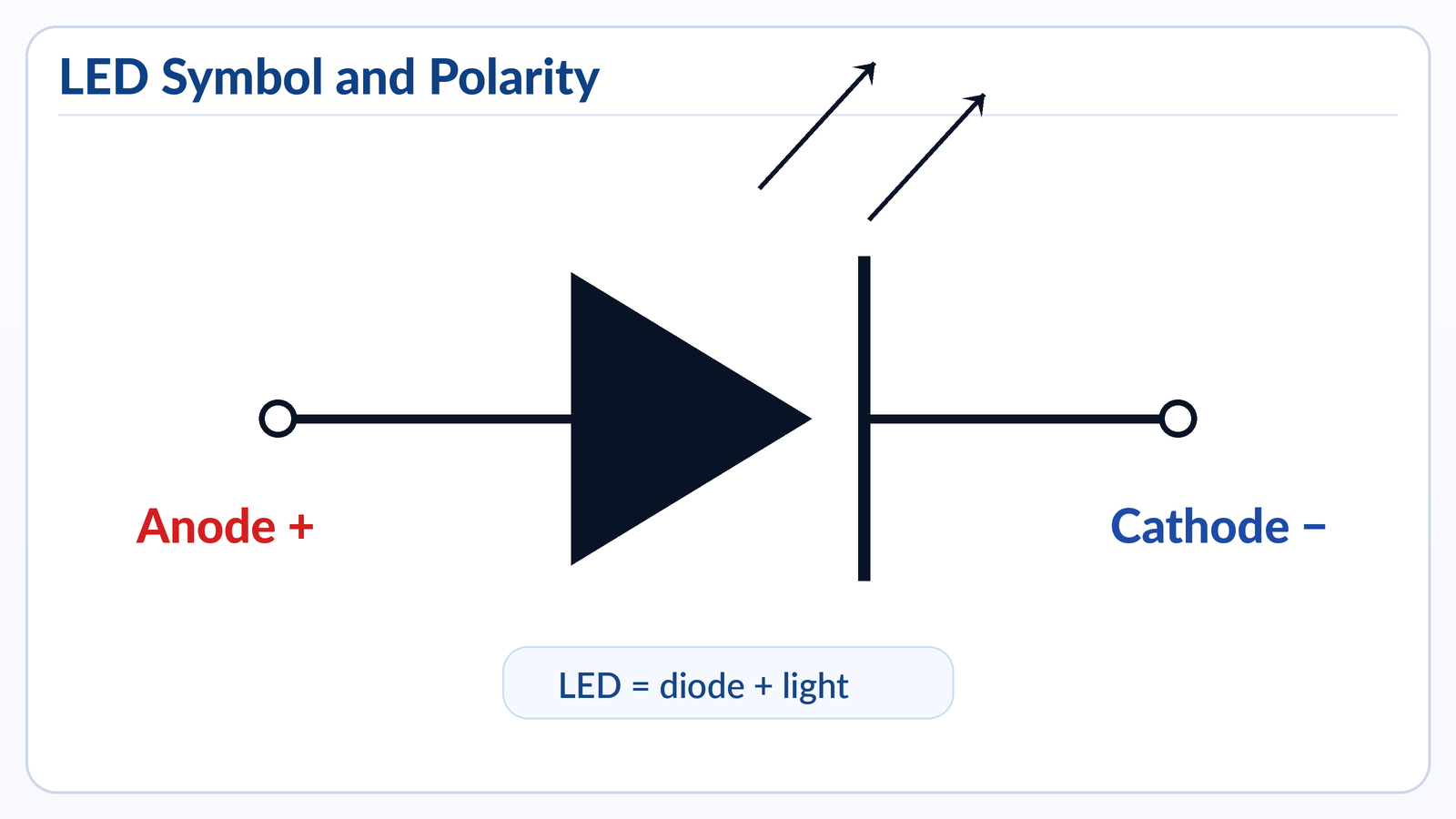
An LED symbol is the schematic representation of a light-emitting diode. Its diode element indicates a polarized semiconductor junction, while two arrows pointing away from the device indicate emitted light. The bar side marks the cathode in the schematic; the opposite terminal is the anode. Designers commonly assign the reference designator D, such as D1 or D12, although some libraries use LED-specific prefixes.

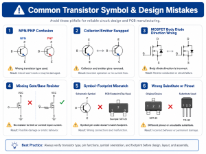
The symbol is only one part of the component definition. A complete CAD record should also include the manufacturer part number, electrical model, package, pin numbers, PCB land pattern and assembly data. If the schematic symbol has anode on pin 1 but the footprint maps pin 1 to the physical cathode pad, the drawing can look correct while the assembled board is wrong.

What Do the Arrows on an LED Symbol Mean?

The two arrows show that the device converts electrical energy into emitted light. Their direction distinguishes the LED from a photodiode: LED arrows point outward, while photodiode arrows point toward the junction because a photodiode receives light. A standard rectifier or signal diode has no light arrows.
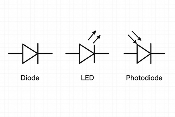
LED symbol compared with diode and photodiode symbols

Arrow direction describes optical function, not current direction. Conventional forward current enters the anode and leaves the cathode. The cathode bar remains the reliable schematic cue when the arrows are small or when a dense drawing is viewed at reduced scale.

How Does an LED Work in a Circuit?

An LED emits light when it is forward biased and current passes through its semiconductor junction. The supply must raise the anode above the cathode by approximately the device’s forward voltage, VF. Forward voltage varies with semiconductor material, color, current and junction temperature, so a nominal value from a generic chart is not a substitute for the selected LED datasheet.

A resistor, constant-current driver or regulated switching stage must control current. Connecting a bare LED directly across a stiff voltage source can produce thermal runaway or immediate overcurrent damage. For PWM dimming, verify peak current, duty cycle, driver timing and the LED’s pulsed-current limits rather than assuming that a low average current makes every pulse safe.

How Do You Identify LED Symbol Polarity?

In the schematic, the cathode is the terminal at the bar and the anode is the opposite terminal. On a common through-hole LED, the longer lead is often the anode and a flat on the body often indicates the cathode. These physical cues are useful during prototyping, but leads may be trimmed and package conventions can vary.
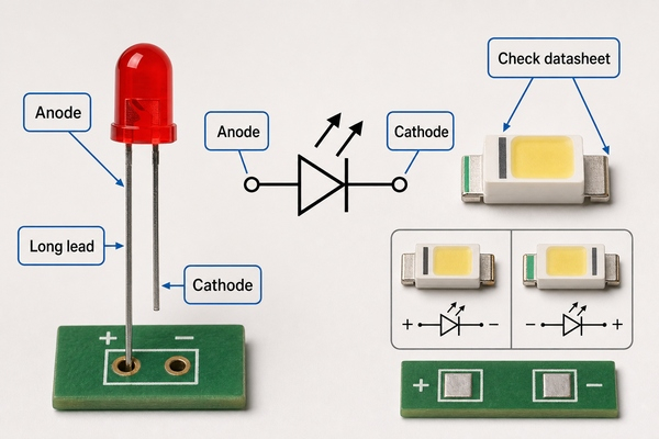
LED symbol polarity with anode cathode through-hole and SMD identification

SMD LED polarity marks are package-specific. A notch, chamfer, colored stripe, internal electrode shape or printed mark may identify one terminal, but the same-looking mark is not guaranteed to mean the same thing across suppliers. Confirm the polarity diagram and recommended land pattern in the exact manufacturer datasheet, then make the schematic pin numbers, footprint pad numbers, silkscreen and pick-and-place rotation agree.

How Is an LED Symbol Used in a Circuit Diagram?

The led symbol circuit connection should make four relationships unambiguous: the drive source, the current-control element, the return path and the polarity. A simple indicator may place the LED and resistor between a logic output and ground. A low-side transistor driver places the LED load toward the supply and switches the return path. A high-side driver reverses that arrangement. In each case, the symbol orientation must reflect the intended conventional current path.

Net labels should identify important rails and control signals, while reference designators allow the BOM, placement file and test procedure to refer to the same component. When several colors or status channels are present, include color or function in the schematic notes, such as STATUS_GREEN or FAULT_RED, rather than expecting assembly staff to infer function from the symbol.

What Is the Difference Between an LED, Diode and Photodiode Symbol?

Device Symbol cue Primary circuit role Design detail to verify
Standard diode Diode element without light arrows Rectification, clamping or switching Forward current, reverse voltage and recovery behavior
LED Two arrows pointing outward Light emission, indication or illumination Forward voltage, current, color, optical output and thermal limit
Photodiode Two arrows pointing inward Optical sensing Bias mode, dark current, spectral response and amplifier interface

A schematic library should not reuse one symbol interchangeably for all three devices. Even when the footprint is similar, their electrical limits, test conditions and functional intent differ. Clear symbols also reduce review errors when a design contains emitters and optical receivers in the same circuit.

What Do Single-Color, Bicolor and RGB LED Symbols Show?

A single-color LED normally has one junction and two pins. A two-lead bicolor LED can contain two dies connected in inverse parallel; reversing current changes the active color. A three-lead bicolor device may use a common anode or common cathode. RGB LEDs commonly have four leads for red, green and blue channels plus a shared terminal, although addressable RGB packages may integrate a controller and use power, ground and data pins instead.

The schematic must show the actual internal connection. A generic three-diode drawing cannot tell assembly or firmware teams whether the package is common-anode, common-cathode or independently connected. Use the selected part’s pin numbering, give each color channel its own current-control element when required, and verify that the PCB footprint orientation matches the datasheet top-view or bottom-view convention.

What Information Does the LED Symbol Not Show?

The graphic does not specify forward voltage, rated current, luminous intensity, wavelength, viewing angle, reverse-voltage limit, ESD sensitivity, package dimensions or thermal resistance. It also does not establish whether the component is suitable for reflow, wave soldering, hand soldering or a particular cleaning process.

The BOM and datasheet must carry those requirements. For color-critical products, define wavelength or chromaticity and binning rather than using only “red” or “white.” For brightness matching, state the relevant optical bin and test current. For power LEDs, include the thermal-pad connection and maximum junction-temperature calculation. The symbol communicates connectivity; it does not replace component qualification.

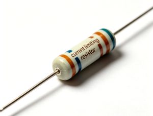
How Do You Calculate an LED Current-Limiting Resistor?

For a simple DC circuit, calculate the series resistor with R = (VS – VF) / IF. If a 5 V rail drives an LED with a 2.0 V forward voltage at 10 mA, the calculated resistance is 300 ohms. Selecting the next higher standard value, such as 330 ohms, reduces current slightly and provides margin for supply and forward-voltage tolerance.
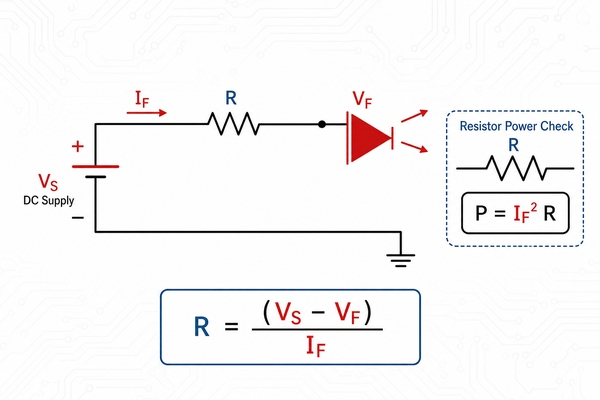
LED symbol circuit with current limiting resistor formula

Check resistor dissipation with P = I2R and apply a sensible derating margin. Calculate worst cases using maximum supply voltage and minimum LED forward voltage for peak current, then minimum supply voltage and maximum forward voltage for minimum brightness. Separate current control is normally preferred for parallel LED branches because normal VF variation can make one branch take disproportionate current.

How Should an LED Footprint and Polarity Mark Be Designed on a PCB?

Start with the manufacturer-recommended land pattern, then check courtyard, solder-mask expansion, paste apertures and component-to-component spacing against the assembly process. Map anode and cathode pin numbers explicitly between the schematic and footprint. A pin-1 convention is useful only when it agrees with the package drawing and does not conceal the electrical polarity.

Place a visible cathode or anode cue on the silkscreen without printing over exposed copper or solderable pads. If board density removes the silkscreen mark, preserve polarity in the assembly drawing and fabrication documentation. The silkscreen PCB design guide explains practical text and clearance controls. For low-power indicators and control panels, a conventional FR4 printed circuit board is usually appropriate. The footprint still needs enough thermal relief for solderability and enough copper to support the expected current.

How Are SMD and Through-Hole LEDs Assembled?

SMD LEDs are placed from centroid data and package rotation, then reflowed according to the component’s moisture sensitivity, peak-temperature and time-above-liquidus limits. Through-hole LEDs require controlled insertion height, lead forming, polarity checks and either selective, wave or hand soldering. A spacer or mechanical fixture may be needed when optical alignment to a light pipe or panel opening matters.

AOI can verify component presence, orientation marks and visible solder joints, but optical inspection alone does not prove color, brightness or electrical function. Hidden thermal pads may justify X-ray, while a functional test should energize channels at controlled current and confirm the intended color and response. EBest Circuit (Best Technology) supports SMT, THT and mixed assembly, with components down to 01005 where the design and process allow; inspection can combine 3D SPI, AOI, X-ray and functional testing according to the actual risk.

For production that needs component sourcing, placement and test under one controlled workflow, the PCB assembly service covers both fabrication and assembly coordination. The BOM should identify the approved LED manufacturer part number, package, color/bin requirements and permitted substitutes so that a visually similar but electrically different LED is not installed.

What Causes an LED Circuit to Fail?

  • Reverse installation: schematic-to-footprint mapping, pick-and-place rotation or manual insertion places the cathode on the anode pad.
  • Excess current: the resistor or driver was selected from typical values without worst-case supply, temperature and forward-voltage limits.
  • Poor thermal path: a power LED’s thermal pad, copper area, dielectric and heat-sink interface cannot keep junction temperature within limit.
  • Inadequate ESD control: handling or test equipment damages the junction before final functional test.
  • Solder defects: insufficient paste, tombstoning, voiding, cold joints or excessive reflow exposure reduces electrical or thermal reliability.
  • Uncontrolled substitution: a replacement part has different polarity marking, pinout, optical bin or footprint dimensions.

Power LEDs need a board selected for the complete thermal path, not just the substrate name. A metal-core PCB can shorten the path from LED pad to heat sink; EBest Circuit (Best Technology) lists MCPCB thermal conductivity from 0.8 to 3.0 W/mK, subject to stack-up and engineering confirmation. For higher insulation or power-density requirements, a high-power LED ceramic PCB may provide a different thermal and dielectric balance.
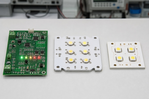
LED PCB materials including FR4 metal core and ceramic boards

Where Are LEDs Used on PCBs?

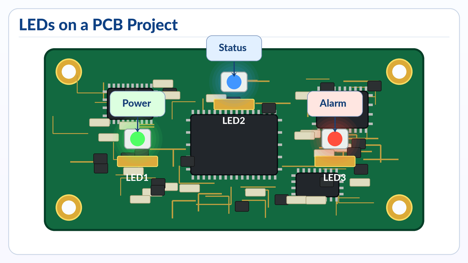
Low-current LEDs provide power, status, fault and communication indicators. Backlight and user-interface boards distribute many LEDs behind light guides or diffusers. Industrial controls use optically visible state confirmation, while sensing systems combine emitters with photodiodes or phototransistors. Automotive, medical and instrumentation products may require controlled color, luminance uniformity, lifetime and environmental validation.

High-power lighting, UV curing, infrared illumination and machine vision place greater demands on current regulation and heat extraction. In these products, the led symbol remains simple, but the board may require an MCPCB, ceramic substrate, thermal vias, direct thermal pads or a mechanically controlled heat-sink interface. Material selection should follow the allowed junction temperature, dissipated power, electrical isolation and assembly process.

FAQ About LED Symbols

Which side of the LED symbol is positive?

The anode is the positive side during normal forward operation. The cathode is the side at the bar in the schematic. Always confirm the physical package mark and pin numbering in the selected component datasheet.

Does the LED symbol show the color?

No. Color may be added as a schematic note or component value, but the symbol itself does not guarantee wavelength or optical bin. Those details belong in the BOM and approved part specification.

Can an LED be connected without a resistor?

Only when another circuit element safely regulates current, such as a constant-current LED driver or a source with an intentionally limited output. A bare LED should not be connected directly across a low-impedance voltage rail.

Is an SMD LED polarity mark universal?

No. Package marks differ among manufacturers and package families. Use the exact datasheet polarity and land-pattern drawing rather than relying on a remembered stripe or notch convention.

Why does an LED work in the prototype but fail after assembly?

Common causes include reversed footprint mapping, pick-and-place rotation, substitute-part pinout differences, reflow damage, ESD, solder defects and insufficient thermal dissipation. Compare the schematic, footprint, BOM, placement file and assembly drawing as one linked data set.

Conclusion

Reading an LED schematic is straightforward once the outward light arrows and cathode bar are recognized, but a reliable board also needs correct pin mapping, controlled current, clear polarity marking, a validated footprint and suitable thermal construction. Treat the symbol, datasheet, BOM, placement data and PCB documentation as one consistent definition.

EBest Circuit (Best Technology) can support FR4, metal-core, ceramic PCB and complete PCBA requirements for LED products. For engineering review or a manufacturing assessment, contact sales@bestpcbs.com.


You may also like

LED Symbol on PCB: Polarity, Identification, and Wiring Guide
Friday, June 26th, 2026

An LED symbol is the standard schematic mark for a light-emitting diode. It looks like a normal diode symbol with two small arrows pointing outward, showing that the component emits light when current flows in the correct direction.

For PCB work, this topic matters because an LED is a polarized component. The anode and cathode must match the circuit and the PCB footprint. A reversed LED may not light, may cause debugging confusion, or may fail if the reverse voltage or current is too high.

Best Technology provides PCB design, PCB prototyping, mass production, component sourcing, and PCB assembly services for LED-related electronics and other custom circuit board projects.

LED Symbol on PCB: Polarity, Identification, and Wiring Guide

What Is the Symbol for LED?

The symbol for an LED is a diode symbol with two arrows pointing away from it. The diode part shows that current flows mainly in one direction, while the outward arrows show light emission.

In a schematic, the LED symbol usually has two sides:

LED Symbol PartMeaningPractical Note
AnodePositive sideCurrent enters here in normal operation
CathodeNegative sideUsually marked by the vertical line/bar side
Two outward arrowsLight outputThis separates LED from a normal diode
Diode bodyOne-way current behaviorLED will not work like a resistor

A simple way to remember it: LED = diode + light arrows.

In circuit diagrams, the LED is often labeled as D, LED, LED1, D1, or sometimes LD. The exact reference designator depends on the designer’s naming rule, but in most PCB documentation, LED components are grouped with diodes because they are part of the diode family.

LED Symbol on PCB

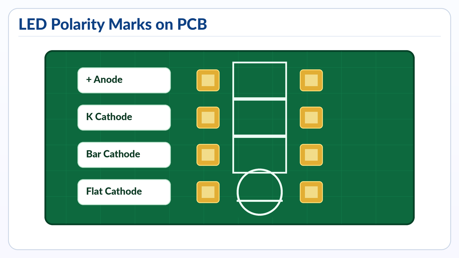
The LED symbol on PCB is usually printed on the silkscreen layer to help assembly workers place the LED in the correct direction. It may appear as a diode symbol, a small outline with a flat side, a “+” mark, a “K” mark, or a cathode bar.

A schematic symbol tells the electrical function. A PCB footprint tells the physical placement. They must match.

Common PCB LED polarity marks include:

PCB MarkingWhat It Usually MeansReliability of Marking
“+” markAnode / positive sideVery clear when used correctly
“K” markCathode sideK comes from “Kathode”
Bar lineCathode sideCommon in diode-style markings
Flat side on outlineCathode side for many through-hole LEDsUseful but package-dependent
Square padOften pin 1, but not always polarityMust check library rule
Dot or chamferPin 1 or cathode/anode depending packageConfirm with datasheet

For through-hole LEDs, the PCB may show a circular outline with one flat edge. This flat edge normally matches the flat side of the LED body, which is commonly the cathode. For SMD LEDs, the polarity mark is often a tiny notch, dot, bevel, green mark, or printed line on the package.

The most common mistake is assuming every PCB library uses the same polarity convention. In real production, this is risky. Some CAD libraries mark pin 1, while the LED datasheet may define pin 1 as cathode or anode depending on the package. Before release, the schematic symbol, PCB footprint, assembly drawing, pick-and-place file, and BOM should all be checked together.

Which Side of the LED Symbol Is Positive?

The positive side of the LED symbol is the anode. In the standard diode-style symbol, the anode is on the side without the vertical bar, and the cathode is on the side with the bar.

The easiest rule is:

Anode = positive side
Cathode = negative side
Cathode side = bar side in the symbol

led symbol on pcb

In normal operation, conventional current flows from the anode to the cathode. That is why the LED only lights when it is forward-biased. If the anode is connected to a higher potential and the cathode is connected through the correct current-limiting path to a lower potential, the LED can turn on.

For real components, polarity can be checked in several ways:

LED TypePositive Side ClueNegative Side Clue
Through-hole LEDLonger lead is usually anodeShorter lead is usually cathode
Round through-hole LEDSmaller internal electrode often anodeLarger internal electrode often cathode
SMD LEDDatasheet defines anode markPackage mark often identifies cathode
PCB footprint“+” often marks anodeBar or “K” often marks cathode

Main Types of LED Symbols and Related Diode Symbols

The LED symbol belongs to the diode symbol family. Different diode types use similar base shapes, but each has extra marks that show its function.

Symbol TypeVisual FeatureMeaningCommon PCB Use
Standard diodeDiode body with barOne-way current flowRectification, reverse protection
LEDDiode body with two arrows pointing outwardEmits lightIndicators, displays, optocouplers, lighting
PhotodiodeDiode body with arrows pointing inwardDetects lightSensors, optical receivers
Zener diodeDiode symbol with bent cathode lineVoltage regulation/clampingReference, surge protection
Schottky diodeModified cathode markingLow forward voltage, fast switchingPower conversion, reverse protection
TVS diodeSuppression-style diode symbolTransient protectionESD and surge protection
Laser diodeLED-like symbol, often with laser indicationCoherent light outputOptical modules, sensors

LED and photodiode symbols are often confused by beginners. The difference is direction of arrows. LED arrows point outward because light leaves the device. Photodiode arrows point inward because light enters the device.

On PCB silkscreen, not every diode type is printed with a full symbol. Some boards use short polarity marks only. For compact boards, especially HDI, wearable electronics, medical modules, and LED driver PCBs, there may be limited space for full silkscreen. In that case, the assembly drawing and component datasheet become even more important.

Which Symbol Is Correct for an LED?

The correct symbol for an LED is a diode symbol with two arrows pointing outward. A plain diode symbol is not technically wrong for showing one-way conduction, but it does not communicate the light-emitting function.

For professional schematics, the LED should use the dedicated LED symbol. This makes the circuit easier to read for engineers, technicians, purchasing teams, and assembly houses.

A correct LED symbol should show:

  • The diode direction
  • The cathode bar
  • The light-emission arrows
  • The reference designator, such as LED1 or D3
  • The value or color, when needed
  • The package or part number in the BOM

For example, an indicator LED might be labeled:

LED1, Green, 0603, 2.0V typical Vf, 20mA max

For a high-power LED, the documentation should be more detailed. It may include forward voltage range, rated current, luminous flux bin, color temperature, thermal pad requirements, and recommended soldering profile.

The symbol alone is not enough for manufacturing. It tells function and polarity, but the PCB assembler also needs the footprint, BOM, polarity mark, and placement data. A clean schematic symbol with a poor footprint can still cause assembly defects.

Which Symbol Is Correct for an LED?

How to Identify LED?

You can identify an LED by checking the package shape, polarity marks, component label, datasheet, and diode-test behavior with a multimeter. For PCB assembly, the datasheet and BOM should always be the final reference.

Common LED identification methods:

MethodHow It WorksBest Use
Look at the circuit symbolLED symbol has outward arrowsReading schematic diagrams
Check PCB silkscreenFind “LED,” “D,” “+,” “K,” or cathode barBoard inspection
Inspect the LED bodyFlat side or short lead often marks cathodeThrough-hole LED identification
Use a multimeter diode modeLED may glow faintly in forward directionBench testing
Check datasheetConfirms pinout, polarity, package, voltageProduction and procurement
Compare BOM and placement fileConfirms exact part usedSMT assembly

For through-hole LEDs, identification is usually simple. The longer leg is commonly positive, and the shorter leg is commonly negative. The flat side on the plastic lens often marks the cathode.

For SMD LEDs, visual identification can be harder. Some packages have a tiny green line, a beveled corner, a dot, or a T-shaped mark. But different manufacturers use different conventions. One 0603 LED may mark the cathode; another may mark the anode. That is why datasheet checking is not optional for mass production.

In PCB manufacturing, a good LED identification process includes component verification before assembly, first article inspection after SMT, and polarity confirmation during AOI or manual inspection. For LED lighting products, additional functional testing is usually needed because a visually correct component can still have color bin, brightness, or forward voltage mismatch issues.

What Is the Element Symbol for LED?

LED does not have a chemical element symbol because it is not a single element. LED stands for Light Emitting Diode, which is an electronic component made from semiconductor materials.

This question often appears because “symbol” can mean two different things:

TermMeaning
LED symbolSchematic symbol used in circuit diagrams
Element symbolChemical abbreviation, such as Cu for copper or Si for silicon
Reference designatorPCB label, such as LED1, D2, or D5
Package markingPhysical mark printed on the LED component

An LED can contain materials such as gallium arsenide, gallium phosphide, gallium nitride, indium gallium nitride, or aluminum gallium indium phosphide, depending on color and performance. But the component itself is not represented by one chemical element symbol.

In schematic and PCB documentation, the more useful identifiers are the circuit symbol, reference designator, manufacturer part number, and package footprint. For procurement, the part number matters more than the generic name. For assembly, the footprint and polarity mark matter more than the visual symbol alone.

How to Tell Which LED Wire Is Positive?

For a typical through-hole LED, the longer wire is the positive side, also called the anode. The shorter wire is the negative side, also called the cathode.

You can also check the LED body. Many round LEDs have a flat side on the rim. That flat side usually marks the cathode. Inside the transparent lens, the larger metal cup is usually the cathode, while the smaller internal electrode is often the anode.

Here is a practical checklist:

ClueUsually Indicates
Longer leadAnode / positive
Shorter leadCathode / negative
Flat side on LED bodyCathode / negative
Larger internal metal cupCathode / negative
PCB “+” markAnode / positive
PCB bar or “K”Cathode / negative

For new parts, these rules work well most of the time. For trimmed leads, recycled parts, custom LEDs, or already-mounted components, use a multimeter in diode mode. Connect the red probe to one lead and the black probe to the other. If the LED glows faintly or shows a forward voltage reading, the red probe is on the anode and the black probe is on the cathode.

Never test a bare LED directly with a high-current power supply unless you use a current-limiting resistor or a controlled LED tester. LEDs are current-driven devices. Too much current can damage the junction quickly.

What Happens If You Wire a LED Light Backwards?

If you wire an LED backwards, it will usually not light because it is reverse-biased. In low-voltage circuits, it may simply stay off. In higher-voltage or poorly protected circuits, reverse bias can damage the LED.

The result depends on the circuit:

SituationLikely Result
Low voltage with current limitLED does not light
Reverse voltage above LED ratingLED may break down
No current-limiting resistorLED may fail when corrected or during fault
LED array wired incorrectlyOne LED may stop an entire string
High-power LED on MCPCBHeat and electrical stress may cause early failure
Reverse polarity in finished PCBAFunctional test failure or field return

Many small indicator LEDs have a limited reverse voltage rating, often around a few volts depending on the datasheet. Once reverse stress exceeds the rating, leakage current can increase and the LED junction may degrade. The component may not fail immediately, but its brightness, stability, or service life can be affected.

For PCB designers, reverse polarity risk can be reduced by adding clear silkscreen marks, using keyed connectors, checking schematic-to-footprint mapping, and including polarity inspection in the assembly process. For LED driver boards, protection design is also important, especially when connectors may be installed by end users.

What Is the Difference Between LED and LCD?

LED and LCD are different technologies. An LED emits light directly, while an LCD controls light but usually needs a backlight to be visible.

ItemLEDLCD
Full nameLight Emitting DiodeLiquid Crystal Display
Basic functionEmits lightControls light transmission
Needs backlight?No for a single LED indicatorUsually yes
PCB roleIndicator, lighting source, display segment, backlightDisplay module with driver circuit
PolarityYes, LED is polarizedLCD module has pin orientation and power requirements
Common usePower indicator, status light, lamps, displaysScreens, meters, panels, instruments

In everyday language, “LED display” and “LCD display” are sometimes used loosely. Many so-called LED TVs are actually LCD panels with LED backlighting. The LED is the light source, while the LCD panel forms the image.

On a PCB, an LED is normally treated as a diode component. An LCD is usually treated as a display module or connectorized assembly. It may include driver ICs, backlight LEDs, flexible cables, zebra connectors, or surface-mounted connectors. Their schematic symbols, footprints, BOM requirements, and inspection methods are different.

LED Symbol and PCB Polarity Design Tips

A correct LED circuit is not only about the schematic symbol. The PCB footprint, silkscreen, copper layout, resistor placement, and assembly documents must all support the same polarity rule.

For indicator LEDs, place the current-limiting resistor close enough to make the circuit easy to follow. For dense PCBs, keep the LED reference designator visible whenever possible. If the board has many LEDs in an array, use consistent orientation so inspection is faster.

For production-ready PCB files, check these points before release:

Design ItemGood PracticeWhy It Matters
Schematic symbolUse true LED symbol with cathode barAvoids confusion with normal diode
Footprint polarityMatch datasheet pinoutPrevents reversed placement
SilkscreenMark “+,” “K,” bar, or flat side clearlyHelps manual and visual inspection
BOMInclude exact manufacturer part numberAvoids color/package mismatch
Pick-and-place fileCorrect rotation and centroidReduces SMT placement errors
Assembly drawingShow polarity for LED partsSupports first article inspection
Test planInclude LED function testCatches reversed or wrong-color LEDs

For SMD LEDs, rotation is a common production issue. A footprint may look symmetric, but the LED is electrically polarized. If the centroid file uses a different zero-degree orientation from the assembler’s machine library, the LED can be rotated incorrectly. This is why first article inspection is important before full production.

Common LED Symbol and Assembly Mistakes

LED-related PCB mistakes are often small, but they can create visible product defects. A reversed resistor may not matter, but a reversed LED usually matters immediately.

Common mistakes include:

MistakeCauseResultPrevention
Reversed LED footprintSymbol pin mapping does not match packageLED does not lightCompare schematic, footprint, and datasheet
Wrong silkscreen mark“+” placed on wrong padAssembly confusionReview polarity on assembly drawing
Missing current-limiting resistorLED connected directly to supplyLED burnoutCalculate resistor or use LED driver
Wrong LED colorBOM not specific enoughVisual mismatchInclude part number, wavelength, CCT, bin
Incorrect SMD rotationPlacement angle mismatchBatch failure riskConfirm first article before mass run
Weak thermal pathHigh-power LED on poor copper designBrightness decay, heat damageUse MCPCB, copper core PCB, or thermal vias as needed
No functional testVisual inspection onlyHidden polarity or brightness issueAdd power-on LED test

For high-power LED PCB design, thermal management becomes part of electrical reliability. The symbol may look simple, but the PCB structure may need aluminum PCB, copper core PCB, heavy copper copper paths, thermal vias, or direct thermal pad design. LED lifetime is strongly affected by junction temperature, so layout and material choice should not be treated as secondary details.

For small signal LEDs, the most useful improvement is documentation clarity. A clean polarity mark can save hours of troubleshooting in prototypes and reduce assembly questions in volume production.

LED Symbol in Real PCB and PCBA Projects

In real projects, the LED symbol appears in many more places than simple breadboard circuits. It is used in consumer electronics, medical devices, industrial controllers, automotive dashboards, communication equipment, power supplies, IoT products, LED lighting, and test fixtures.

Typical LED use cases include:

ApplicationLED FunctionPCB Design Concern
Power supply boardPower-on indicatorResistor value, visibility, polarity
Industrial controllerStatus signalLabel clarity, EMI environment, serviceability
Medical device PCBAAlarm or state indicationReliability, color consistency, inspection
Automotive switch panelBacklight or indicatorTemperature, vibration, lifetime
LED lighting boardMain light sourceThermal path, current control, material choice
Communication equipmentPort status LEDPlacement accuracy, light pipe alignment
Test fixtureDebug indicatorEasy probing and replacement

In a prototype, an LED is often used as a quick debugging tool. Engineers may add LEDs to show power rails, MCU status, communication activity, charging state, or fault conditions. In production, those LEDs must be reviewed carefully. Debug LEDs may increase cost, power consumption, assembly time, or light leakage. Some are removed before mass production, while others are kept for service diagnostics.

For PCB buyers, LED-related details should be included in the quotation package when they affect assembly. The Gerber file alone may show pads and silkscreen, but it does not confirm the exact LED color, brightness, viewing angle, polarity mark, packaging reel direction, or test requirements.

How to Prepare LED PCB Files for Manufacturing

For LED PCB or PCBA production, clear files reduce quotation delays and assembly risk. The manufacturer should not need to guess LED polarity from a blurry image or incomplete BOM.

A strong file package should include:

  • Gerber files
  • Drill files
  • BOM with manufacturer part numbers
  • Pick-and-place file
  • Assembly drawing
  • Schematic PDF
  • LED datasheets
  • Polarity notes for SMD LEDs
  • Test requirements
  • Lighting performance requirements, if applicable

For LED lighting projects, also provide thermal requirements such as input power, LED current, operating temperature, target lifetime, board material, copper thickness, and heat sink information. For indicator LED projects, provide color, package size, brightness range, and lens or enclosure alignment requirements.

Best Technology supports standard FR4 PCB, multilayer PCB, metal core PCB, ceramic PCB, flexible and rigid-flex PCB, high-frequency PCB, PCB assembly, and component sourcing. The company also lists quality certifications including IATF 16949, ISO 9001:2015, ISO 13485:2016, AS9100D, REACH, RoHS, and UL.

FAQs

What Does the LED Symbol Look Like?

The LED symbol looks like a diode symbol with two small arrows pointing outward. The diode part shows one-way current flow, and the arrows show light emission. The vertical bar side is the cathode, while the other side is the anode. This symbol is used in schematics to separate LEDs from standard diodes, Zener diodes, and photodiodes.

What Does LED Mean in Electronics?

LED means Light Emitting Diode. It is a semiconductor component that emits light when current flows through it in the forward direction. Because it is a diode, it has polarity. The positive side is called the anode, and the negative side is called the cathode. It is widely used for indicators, displays, backlighting, and lighting systems.

Is the Arrow on an LED Symbol the Current Direction?

The diode body in the LED symbol shows the normal forward direction from anode to cathode for conventional current. The two small arrows pointing away from the symbol do not show current direction. They show emitted light. This is an important distinction because beginners sometimes read the light arrows as electrical direction, which can lead to wrong polarity decisions.

Which Side Is Negative on an LED Symbol?

The negative side of an LED symbol is the cathode. In the standard symbol, the cathode is the side with the vertical bar. On a PCB, the cathode may be marked with a bar, “K,” flat side, dot, or package mark. For mass production, always check the LED datasheet and the PCB footprint pin mapping.

Does the Flat Side of an LED Mean Negative?

For many round through-hole LEDs, the flat side of the plastic body marks the negative side, or cathode. The shorter lead also usually marks the cathode. However, this rule should be used with care for special LEDs, trimmed leads, and SMD packages. For production, the datasheet is more reliable than visual inspection alone.

Can an LED Work Without a Resistor?

An LED should not be connected directly to a voltage source unless the circuit already includes current control. A resistor or LED driver is normally used to limit current. Without current limiting, the LED may draw too much current and fail. The resistor value depends on supply voltage, LED forward voltage, and target current.

Why Does My LED Not Light on the PCB?

The LED may not light because it is reversed, the resistor value is too high, the supply voltage is missing, the solder joint is poor, the LED is damaged, or the wrong part was assembled. Start by checking polarity, forward voltage, current path, and solder quality. Then compare the schematic, PCB footprint, BOM, and datasheet.

How Do I Test LED Polarity With a Multimeter?

Set the multimeter to diode mode. Touch the red probe to one LED lead and the black probe to the other. If the LED glows faintly or shows a forward voltage reading, the red probe is on the anode and the black probe is on the cathode. If it does not respond, reverse the probes and test again.

Is LED an AC or DC Component?

An LED is normally driven by DC current in the forward direction. It can be used in AC circuits only with proper protection, rectification, or current limiting. Direct reverse voltage from AC can damage an LED if it exceeds the rated limit. LED lamps for AC mains include driver circuits, not just bare LEDs.

What Is the Difference Between Anode and Cathode in an LED?

The anode is the positive side of the LED during normal forward operation. The cathode is the negative side. Current flows from anode to cathode, and the LED emits light when the forward voltage and current are suitable. On the schematic symbol, the cathode is usually shown by the vertical bar.

Why Are LED Symbols Printed on PCB Silkscreen?

LED symbols or polarity marks are printed on PCB silkscreen to guide assembly and inspection. Since LEDs are polarized, the assembler must know which pad is anode and which pad is cathode. Clear silkscreen helps prevent reversed placement, especially during manual soldering, prototype builds, rework, and first article inspection.

Are All SMD LED Polarity Marks the Same?

No. SMD LED polarity marks vary by manufacturer and package. Some marks indicate the cathode, while others may indicate the anode or pin 1. The mark may be a dot, line, notch, bevel, or colored area. For SMT production, the datasheet and confirmed pick-and-place orientation are essential.

What Does K Mean on an LED PCB Footprint?

“K” usually means cathode. It comes from the German word “Kathode.” If a PCB footprint has a “K” mark beside one pad, that pad should connect to the negative side of the LED in normal operation. Even so, it is good practice to compare the footprint with the schematic and LED datasheet.

Can a Reversed LED Damage a Circuit?

A reversed LED often just stays off in low-voltage circuits. However, if the reverse voltage is too high or the circuit has poor current protection, the LED can fail. In LED strings, one reversed LED can stop the entire string from lighting. In finished products, reversed LEDs usually cause functional test failure.

What Should I Send to a PCB Manufacturer for LED Assembly?

Send Gerber files, BOM, pick-and-place file, assembly drawing, schematic PDF, LED datasheets, polarity notes, and test requirements. For high-power LED boards, also provide current, power, thermal requirements, board material preference, copper thickness, and operating environment. Clear documentation helps reduce assembly errors and quotation delays.

Conclusion

The LED symbol is simple, but its manufacturing meaning is important. It shows a polarized light-emitting diode, with the anode as the positive side and the cathode as the bar side. On a PCB, that symbol must match the footprint, silkscreen, BOM, datasheet, and placement file.

For design and purchasing teams, the safest approach is to treat LED polarity as a controlled assembly detail, not a visual guess. Check the schematic-to-footprint mapping, confirm SMD polarity marks, use current limiting, and include LED function testing when the product depends on visible status or lighting performance.

If you’re sourcing reliable PCB/PCBA manufacturing — OEM, ODM, prototyping, mass production, or custom engineering solutions — reach out to our engineering team for technical support and a quote at sales@bestpcbs.com.

You may also like