PCB manufacturing PCB manufacturing
Home > Blog

2N2222 Pinout Guide for PCB Layout and PCBA Assembly

August 3rd, 2026

2N2222 pinout looks like a small three-pin detail, but it can decide whether a transistor footprint, BOM substitute, and assembled PCBA work correctly after production. For PCB buyers and engineers, the main risk is not knowing that the same transistor name may appear in different packages, views, or supplier drawings.

Before PCB fabrication or PCBA assembly, the emitter, base, and collector must match the exact datasheet, package outline, PCB footprint, silkscreen mark, and assembly direction. A wrong pin order can pass a quick visual check but fail during functional testing, rework, or field use.

EBest Circuit (Best Technology) supports PCB fabrication, PCB layout manufacturability review, component sourcing coordination, PCBA assembly, inspection, and testing support for transistor-based control boards. If you need help checking a 2N2222 transistor footprint or assembly file before production, contact sales@bestpcbs.com.

2N2222 pinout
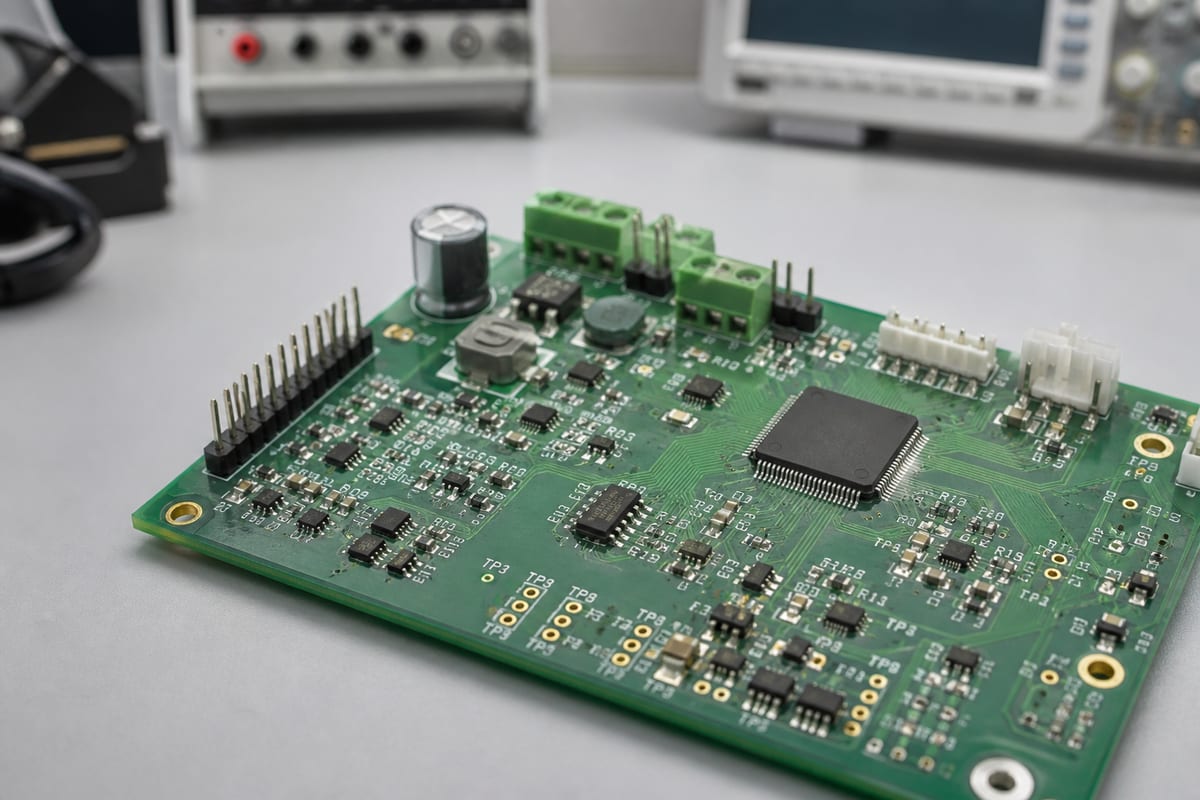
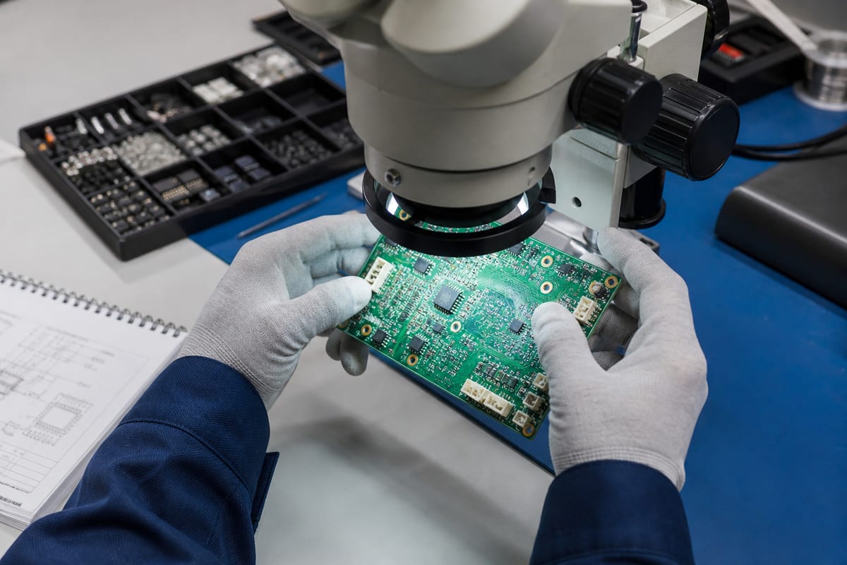
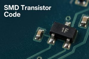
2N2222 pinout review should connect the transistor package, footprint, BOM, and PCBA assembly direction.

What Is the 2N2222 Pinout?

The 2N2222 pinout is the pin assignment for the three terminals of a 2N2222 NPN bipolar junction transistor. The terminals are emitter, base, and collector.

The simple explanation is:

  • Emitter: current exits the transistor in typical NPN switching circuits.
  • Base: receives the control signal through a suitable resistor.
  • Collector: connects to the load side in many low-power switching designs.

That sounds simple, but it is not enough for production. The pin order depends on the exact part number, package, manufacturer datasheet, and how the transistor is viewed. A TO-92 part shown from the flat face may not match a metal-can package or an SMD package. Even similar names such as 2N2222A, PN2222A, and P2N2222A should be checked against the selected manufacturer datasheet.

For a PCB or PCBA order, the safest wording is not “2N2222 is always E-B-C.” The safer production instruction is: confirm the manufacturer part number, package, pin view, PCB footprint, and assembly orientation before release.

2N2222 Transistor Pinout and Pin Functions

A 2N2222 transistor is commonly used as a small-signal NPN transistor for switching and amplification. In many PCB products, it may drive LEDs, relays, buzzers, small motors, signal lines, or interface circuits.

Buyers usually need to confirm these pin functions before PCBA:

Pin Function What to Check in Production Files Risk if Wrong
Emitter Connected to the correct reference or return path. The transistor may not switch correctly.
Base Controlled through the correct resistor network. The transistor may stay off, overheat, or behave unstably.
Collector Matched to the load side and current path. The load may fail to operate or the part may be damaged.

For assembly teams, the pin function is only useful when it is tied to the physical footprint. A schematic may be correct, but the PCB symbol-to-footprint mapping can still be wrong. This is why transistor pinout checks should include the schematic symbol, PCB footprint pads, BOM manufacturer part number, and placement drawing.

2N2222 Pin Configuration by Package Type

The phrase “2N2222 pin configuration” often creates confusion because users may be looking at different package types. A TO-92 plastic package, TO-18 metal can, and SMD transistor package cannot be treated as one fixed layout.

Common package review points include:

  • TO-92: confirm whether the drawing is viewed from the flat face or lead side.
  • TO-18 metal can: confirm the bottom-view or top-view reference in the datasheet.
  • SOT-23 or other SMD substitutes: confirm the exact substitute part and footprint.
  • PN2222A or P2N2222A: do not assume the same pin order as another supplier’s 2N2222.

In real sourcing work, the project may start with “2N2222” in the BOM, but the available part may be a manufacturer-specific 2N2222A, PN2222A, P2N2222A, or SMD equivalent. The electrical replacement may look acceptable, but the footprint and pin order still need a separate check.

2N2222 pinout
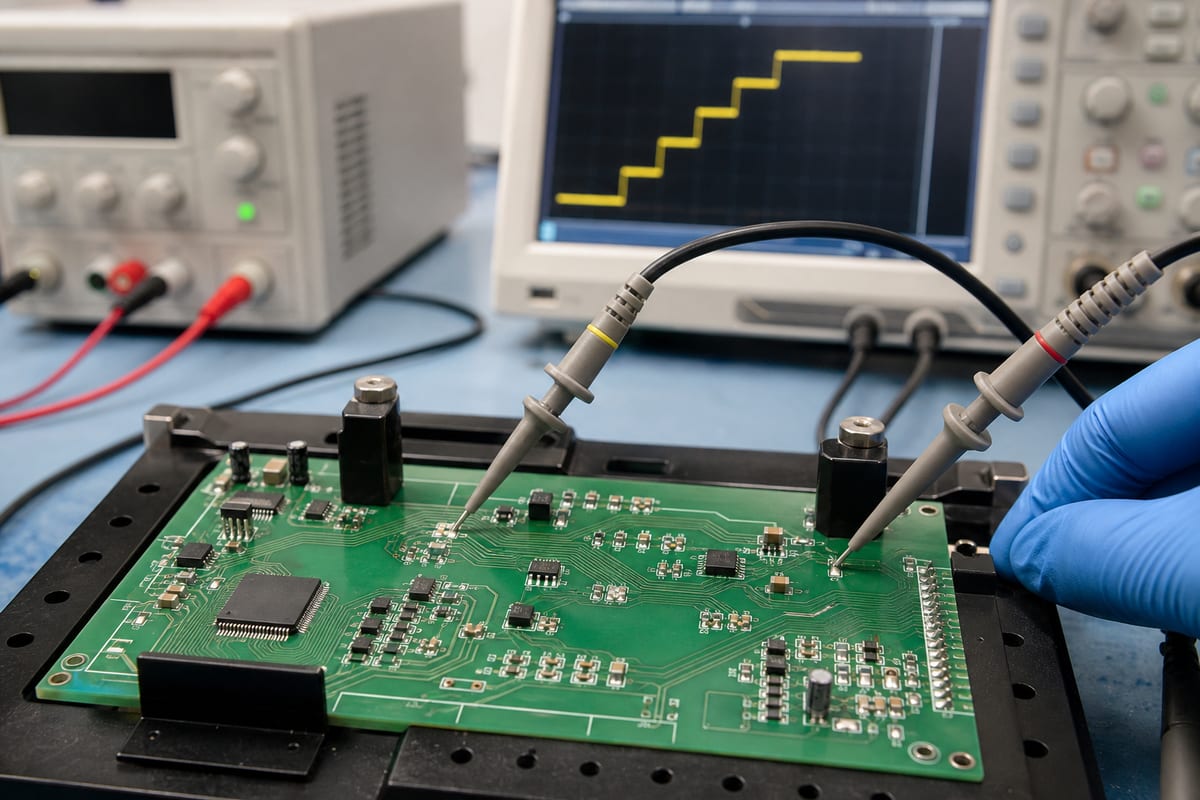
Always confirm the exact datasheet view before releasing the transistor footprint for PCB layout or PCBA assembly.

2N2222 Pin Diagram Mistakes Before PCB Layout

A 2N2222 pin diagram can be correct on its own but still cause a wrong PCB if the view direction is misunderstood. Many drawings show the package from a specific side, and that side is easy to reverse during footprint creation.

Common mistakes before layout include:

  • Reading a bottom-view drawing as a top-view drawing.
  • Copying a generic internet pinout without checking the chosen manufacturer.
  • Using a TO-92 footprint for a different lead order.
  • Replacing a through-hole part with an SMD part without footprint review.
  • Leaving the flat-side mark unclear on the silkscreen.
  • Letting the BOM name and assembly drawing describe different packages.

For a single prototype, one wrong footprint may be repaired by cutting traces or bending leads. For a batch build, the same error can stop assembly, delay shipment, and create extra component and labor cost.

A practical DFM review should ask one direct question: if an operator looks at the PCB, BOM, and placement drawing, can they install the transistor in only one correct orientation?

2N2222A Pinout and PN2222A Pinout Differences

2N2222A and PN2222A are often discussed together because both are common NPN transistor options. However, their pinout should not be judged only by the name. The package and manufacturer matter.

For BOM substitution, check these items before approval:

  • Full manufacturer part number
  • Package code and drawing
  • Pin assignment and view direction
  • Collector current and voltage rating
  • Power dissipation and thermal condition
  • Gain range or hFE grouping
  • Lead forming or tape packaging requirement
  • Footprint compatibility with the PCB

From the buyer’s side, this is where component sourcing and assembly review should work together. A purchasing team may find an available substitute, but the engineering review must confirm whether it can be assembled on the same PCB without changing the footprint or circuit behavior.

EBest Circuit can help flag these sourcing-related manufacturing risks before production. The final electrical approval should still come from the customer’s engineering team, especially when the transistor is used near its voltage, current, gain, or thermal limits.

How to Check the 2N2222 Datasheet Before PCB Footprint Selection

The datasheet is the authority for footprint selection. Search results and quick diagrams can help explain the topic, but they should not replace the selected manufacturer’s datasheet in a production build.

A datasheet check should confirm:

  • Exact package outline
  • Lead order and view direction
  • Recommended mounting style
  • Lead diameter or pad geometry
  • Body size and height
  • Thermal limits
  • Electrical rating margin
  • Storage and soldering conditions

For through-hole designs, the footprint must match lead spacing, hole size, annular ring, soldering method, and component height. For SMD alternatives, the pad size, solder mask opening, stencil opening, and placement rotation must be reviewed.

This is also a good place to check whether the board will use FR4 PCB, high-current copper requirements, special soldering conditions, or mechanical constraints around the transistor body. The transistor may be small, but its placement can affect test access, repair access, heat concentration, and enclosure clearance.

PCB Layout Checks for a 2N2222 Transistor

PCB layout checks for a 2N2222 transistor should focus on the physical connection between schematic intent and manufacturable board data. A correct circuit on paper can still fail if the footprint, routing, or silkscreen creates assembly ambiguity.

Layout checks should include:

  • Pin mapping between schematic symbol and PCB footprint
  • Clear emitter, base, and collector pad assignment
  • Readable silkscreen orientation mark
  • Correct base resistor placement and routing
  • Load current path and copper width
  • Thermal spacing from heat-sensitive components
  • Test point access for important signals
  • Enough clearance for hand insertion or AOI review
  • No conflict between the BOM package and footprint package

For low-current signal switching, the copper requirement may be modest. For relay drive, LED arrays, motor control, or solenoid-related circuits, the current path and heat condition deserve closer attention. The PCB supplier should not redesign the circuit, but can flag layout and manufacturing issues that may affect assembly quality or repeatability.

PCBA Assembly Checks for 2N2222 Pinout and Orientation

During PCBA assembly, the 2N2222 transistor must be placed in the correct orientation and soldered with a stable process. The assembly drawing should show the package direction clearly enough that operators and inspectors do not need to guess.

Assembly checks should cover:

  • Correct transistor part number loaded for production
  • Package match between BOM and PCB footprint
  • Lead forming direction for through-hole parts
  • Placement rotation for SMD parts
  • Polarity or orientation mark on silkscreen
  • Solder joint quality after reflow, wave soldering, or hand soldering
  • AOI or visual inspection access
  • Functional test coverage after assembly

For through-hole assembly, the main concerns are lead spacing, hole fit, solder fill, component height, and post-solder inspection. For SMT assembly, the main concerns are rotation, pad size, stencil opening, component availability, and AOI recognition.

2N2222 pinout
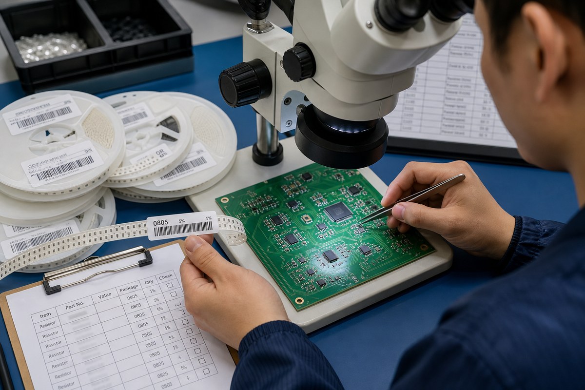
PCBA assembly review should confirm transistor orientation, soldering quality, inspection access, and final functional test coverage.

A small transistor can be difficult to inspect after it is surrounded by taller components, connectors, heatsinks, or enclosure hardware. Good layout and assembly planning make inspection and rework easier before the board reaches the final product stage.

2N2222 Pinout Project Example for a Small Control PCB

A practical 2N2222-related PCBA project may begin with a very simple request: “Please assemble this control board.” The real manufacturing risk appears when the BOM, footprint, and component supply are checked together.

A customer developing a small industrial control PCB needed a 2N2222-family transistor to drive a buzzer and an indicator output. The first sample quantity was 50 pieces for functional validation, followed by a planned small batch after enclosure testing. The board used FR4 material, mixed SMT and through-hole parts, terminal blocks, LEDs, and several discrete components.

Project details:

  • Application: compact industrial control module
  • Quantity: 50 prototype PCBAs before small-batch production
  • Board type: FR4 PCB with mixed assembly
  • Main component concern: 2N2222-family transistor availability and orientation
  • Assembly needs: SMT placement, through-hole assembly, visual inspection, and functional test support
  • Delivery focus: quick prototype build for circuit and enclosure validation

During file review, the schematic symbol looked correct, but the BOM used a supplier-specific 2N2222A part while the footprint appeared to be copied from another TO-92 transistor. The customer also allowed substitute parts if the original part was unavailable. That created a real risk: a substitute could meet the electrical requirement but use a different pin order or package drawing.

Main checks before production:

  • Matched the BOM part number against the selected package drawing.
  • Checked emitter, base, and collector mapping against the PCB pads.
  • Flagged substitute approval as an engineering review item, not only a purchasing item.
  • Confirmed the transistor orientation mark on the assembly drawing.
  • Added functional test attention for the buzzer and indicator output.

This type of review does not change the customer’s circuit design. It protects the manufacturing result by making sure the approved design data, purchased component, PCB footprint, and assembly process all describe the same physical part.

For buyers, the value is practical: fewer assembly surprises, fewer emergency footprint corrections, and fewer delays between prototype validation and small-batch production.

FAQs About 2N2222 Pinout

Is the 2N2222 pinout always the same?
No. The pinout depends on the exact part number, package, manufacturer datasheet, and view direction. Always confirm the selected datasheet before PCB footprint release.

What are the three pins of a 2N2222 transistor?
The three terminals are emitter, base, and collector. Their physical order must be checked against the exact package drawing.

Is 2N2222A the same as PN2222A?
They are related NPN transistor options, but buyers should not assume identical package, pin order, or manufacturer specifications without datasheet review.

Can a wrong 2N2222 footprint cause PCBA failure?
Yes. A wrong footprint or reversed pin mapping can stop the transistor from switching correctly and may require rework or PCB revision.

Can EBest Circuit check 2N2222 orientation before assembly?
Yes. EBest Circuit can support PCB layout manufacturability review, BOM and footprint checks, PCBA assembly, inspection, and functional testing support based on customer-approved files.

In Conclusion, 2N2222 pinout affects more than a symbol on the schematic. It affects footprint selection, BOM substitution, silkscreen direction, soldering quality, inspection, and functional test results. Before PCB fabrication or PCBA assembly, confirm the exact datasheet, package, pin view, and assembly orientation.

EBest Circuit (Best Technology) supports PCB fabrication, PCB layout manufacturability review, component sourcing coordination, PCBA assembly, inspection, and testing support for transistor-based boards. For project review, send Gerber files, BOM, pick-and-place file, assembly drawing, and test requirements to sales@bestpcbs.com.

You may also like

PLCC Package: PCB Footprint, Soldering, and Assembly Guide

July 31st, 2026

A PLCC package is a plastic leaded chip carrier with J-shaped leads folded under the package body. It can be mounted in a socket or soldered directly to a printed circuit board. That flexibility made PLCC devices common in memory, controllers, processors, programmable logic, and many long-life industrial products.

For a PCB assembly buyer, however, recognizing the package name is only the beginning. The exact manufacturer part number, pin count, body dimensions, land pattern, Pin 1 orientation, component supply condition, soldering process, and inspection method must all agree. A PLCC component that looks correct can still be the wrong ordering code or a poor match for the released footprint.

This guide explains the package from a PCB and PCBA manufacturing perspective. It shows what engineers and buyers should confirm before component sourcing, stencil release, assembly, inspection, rework, and repeat production.

plcc package
PLCC package review should connect the component drawing, PCB footprint, sourcing data, and assembly plan.

What Is a PLCC Package?

PLCC means plastic leaded chip carrier. The package usually has leads on four sides, with each lead curling inward beneath the molded body in a J shape. Unlike a leadless chip carrier, a PLCC has formed metal leads. Unlike a typical QFP, its leads do not extend outward as long gull-wing terminals.

Many PLCC families use a 1.27 mm lead pitch, but the package name alone does not establish the complete mechanical specification. Different devices can have different pin counts, body sizes, heights, tolerances, ordering codes, moisture-handling requirements, and manufacturer-recommended footprints. The current component datasheet and package drawing must control the build.

PLCC devices may be directly soldered to the PCB or installed in a matching socket. A socket makes component removal or replacement easier, but it also adds height, cost, contacts, and another mechanical interface. Direct soldering creates a lower-profile assembly but makes replacement more dependent on controlled rework.

If an incoming part must be identified from its body markings, use the marking, BOM, manufacturer documentation, package dimensions, and board records together. The PCB components identification guide explains why one visible code is not enough to approve a component for production.

How Does a PLCC Package Connect to a PCB?

A directly soldered PLCC sits over perimeter pads on the PCB. Solder paste is printed on the lands, the component is placed with the correct orientation, and the assembly passes through the approved reflow process. The solder joints form around the exposed lower portions of the J-leads.

The inward lead shape saves board area, but it also changes what can be seen after soldering. Part of each termination is close to or under the package body. This means a board can look generally acceptable from above while still requiring closer inspection of lead wetting, alignment, bridging, insufficient solder, or lifted leads.

A socketed build follows a different path. The PCB is assembled with the PLCC socket, and the IC is inserted later. The socket footprint, socket orientation, insertion method, retention, overall height, and access for removal all become part of the assembly review.

Before choosing the mounting method, confirm:

  • whether the released BOM calls for the IC alone or an IC-and-socket combination;
  • whether field replacement or programming access requires a removable device;
  • whether the enclosure allows the added socket height;
  • whether vibration, contact resistance, thermal cycling, or handling affects the product requirement;
  • whether the production quantity and test flow support manual insertion after reflow.

The customer’s product team remains responsible for the electrical and system-level choice. EBest Circuit (Best Technology) can review the released PCB, BOM, CPL, assembly drawing, and process notes for manufacturing conflicts before PCBA production.

PLCC Package Sizes, Pin Counts, and Footprints

PLCC is a package family, not one universal outline. Common devices include square and rectangular bodies with different pin counts. Manufacturer drawings also define body dimensions, lead pitch, lead width, seating details, tolerances, and the Pin 1 index area.

The risk appears when a BOM uses only a generic description such as “PLCC-44” while the PCB library was created from a different device or socket drawing. The pin count may match, but the body, lead geometry, courtyard, socket requirements, or recommended land pattern may not.

Use this identification chain before approving the footprint:

  • complete manufacturer part number and ordering code;
  • manufacturer and current datasheet revision;
  • package name, pin count, pitch, and drawing code;
  • body width, body length, and maximum seated height;
  • terminal dimensions and recommended PCB land pattern;
  • Pin 1 marking and pin-numbering direction;
  • tube, tray, tape, or other delivery format needed for assembly.

For example, Microchip publishes separate PLCC package outline drawings, while NXP lists package-specific dimensions and mounting details for PLCC families. These sources illustrate why a generic package label should never replace the exact component drawing.

The existing guide to part number width specifications provides a broader method for reconciling ordering codes, package drawings, tolerances, land patterns, and incoming parts.

Socketed vs Soldered PLCC Assembly

Decision Socketed PLCC Directly soldered PLCC
Replacement Easier device removal Requires controlled rework
Assembly height Higher Lower
Interfaces Socket plus IC contacts Solder joints to PCB
Production steps Socket assembly and IC insertion Placement and reflow

A socket is useful when the component must be removed for programming, service, configuration, or replacement. It can also protect the IC from the primary soldering process when the released product plan requires later insertion.

But a socket is not automatically the safer manufacturing option. A mismatched socket, reversed socket, bent contact, incomplete insertion, or excessive insertion force can stop the board at test. Added height may also interfere with an enclosure or neighboring hardware.

Direct soldering eliminates the socket interface and supports automated SMT assembly. The process must still match the component’s approved storage, handling, placement, and reflow requirements. Old or separately sourced PLCC stock should not be released to the line only because the part number appears correct.

For repeat builds, record the approved part, socket if used, footprint revision, orientation image, insertion step, inspection criteria, and any programming sequence. These records reduce the risk of the next lot being built from an incomplete purchasing description.

How Should a PLCC Footprint Be Reviewed?

A footprint review does not redesign the circuit. It compares the released component data with the PCB land pattern and the needs of fabrication, assembly, inspection, and rework.

Key review points include:

  • Land geometry. Compare pad length, width, pitch, and location with the current manufacturer recommendation or the customer-approved library standard.
  • Pin 1 control. The PCB, silkscreen, assembly drawing, CPL rotation, and component marking must communicate the same orientation.
  • Solder mask and paste. Openings must support the released pad and stencil strategy without creating avoidable bridging or insufficient solder risk.
  • Courtyard and access. Nearby components, sockets, connectors, enclosure parts, and rework tools need adequate clearance.
  • Board support. Large packages and sockets should not sit in areas where panel handling, depaneling, or board flex creates unnecessary mechanical stress.
  • Inspection visibility. The layout should allow the planned inspection method to view the relevant lead areas.

A common failure scenario is a correct IC placed on a footprint copied from an unrelated PLCC library entry. The board reaches SMT, but the land geometry or orientation convention does not match the released part. Production then stops for engineering clarification, stencil revision, PCB rework, or a new board revision.

Sending the exact package drawing with the Gerber or ODB++, BOM, CPL, and assembly drawing lets the PCBA supplier raise this conflict before materials and schedules are committed.

plcc package
Footprint and Pin 1 alignment should be confirmed before the PLCC component is released for placement.

Common PLCC Soldering and Assembly Problems

PLCC assembly problems are usually not caused by the package name itself. They come from mismatched data, uncontrolled materials, or a process that does not account for the J-lead geometry.

Wrong orientation. If the CPL rotation, silkscreen mark, drawing, and package index are inconsistent, a correctly sourced component can be placed 90 or 180 degrees from the intended orientation. Clear Pin 1 documentation and first-article confirmation reduce this risk.

Solder bridging. Excess paste, poor alignment, inappropriate stencil openings, contamination, or lead damage can connect adjacent terminations. The consequence may be an immediate electrical short or a board that fails powered testing.

Insufficient solder or poor wetting. Storage condition, surface contamination, lead finish, paste transfer, land geometry, or reflow conditions can leave a weak or incomplete joint. A simple top view may not show the full condition around the J-lead.

Lifted or damaged leads. Improper handling, unsuitable packaging, or uncontrolled rework can deform a lead. The component may still sit on the board while one termination does not contact the land correctly.

Package-to-footprint mismatch. A buyer approves an alternate with the same function and pin count, but the package drawing is different. This can cause placement, soldering, clearance, or inspection problems even before electrical compatibility is considered.

Uncontrolled legacy stock. A part may be obsolete, aged, repacked, or supplied without enough traceability and handling information. The sourcing decision should be completed before the SMT schedule is fixed. See the BestPCBS component sourcing resources for the BOM information buyers should prepare.

How Are PLCC Solder Joints Inspected?

Inspection should answer a defined risk question. It should not be added as a generic line in the quotation without clear coverage.

Visual inspection can check orientation, body damage, obvious offset, exposed lead condition, and visible solder quality. AOI can support repeatable checks for placement, polarity, bridging, and other visible conditions when the package and board geometry provide a usable camera view.

However, AOI cannot prove component function, and the inward J-lead shape limits visibility compared with a long outward gull-wing lead. If the acceptance requirement depends on an area that is not adequately visible, the customer and supplier should agree on another suitable method rather than claiming that AOI proves every joint.

Electrical or functional testing addresses a different question: whether the assembled board behaves according to the customer’s defined test plan. Testing requires suitable test points, firmware or programming files when applicable, fixtures or connection instructions, limits, and pass/fail criteria.

The AOI in PCB manufacturing guide explains how AOI differs from SPI, X-ray, electrical checks, and functional testing.

plcc package
PLCC inspection should combine visible workmanship checks with the electrical or functional test coverage defined by the customer.

PLCC vs QFP and BGA Packages

Package Connection style Manufacturing consideration
PLCC J-leads under body edge Socket option and partial joint visibility
QFP Gull-wing leads extend outward Lead coplanarity and fine-pitch handling
BGA Solder balls under package Hidden joints and X-ray planning

PLCC, QFP, and BGA describe different mechanical connection systems. They should not be treated as interchangeable simply because two devices offer similar electronic functions.

A QFP usually provides more visible solder joints, but its outward leads increase the package footprint and can be vulnerable to handling damage. A BGA supports a high connection count beneath the body, but its joints are hidden and require a different land pattern, stencil strategy, reflow process, and inspection plan.

The package choice belongs to the customer’s electronic and product design team. From the manufacturing side, the important task is to build the released package correctly and identify when the BOM, footprint, placement data, inspection access, and replacement plan do not agree.

What Should You Send for a PLCC PCBA Quote?

A quotation based only on board size, layer count, and the phrase “PLCC assembly” leaves too many assumptions open. A useful RFQ connects the component, PCB, assembly process, inspection, testing, and delivery requirement.

Send these files and decisions:

  • Gerber or ODB++ files, NC drill data, and fabrication drawing;
  • complete BOM with exact manufacturer part numbers and approved alternates;
  • CPL or centroid file with designators, coordinates, side, and rotation;
  • assembly drawing with Pin 1, polarity, no-fit, and special handling notes;
  • PLCC manufacturer datasheet and package drawing;
  • socket manufacturer part number and insertion instructions, if applicable;
  • customer-supplied versus supplier-sourced component responsibility;
  • inspection, programming, functional test, acceptance, and packing requirements;
  • prototype and production quantities plus the requested delivery schedule.

A realistic production example. A buyer requests 100 controller PCBAs using a legacy 44-lead PLCC. The BOM lists a shortened part number, while the PCB library name only says “PLCC44.” One supplier quotes immediately. Another supplier asks for the complete ordering code and package drawing, then finds that the proposed substitute and the released land pattern do not share the same approved mechanical details.

The second supplier has not redesigned the product. It has prevented an unapproved assumption from reaching purchasing and SMT. The buyer can now confirm the exact component, approve a documented alternate, or revise the released footprint before ordering boards and material.

When delivery is urgent, the same principle applies. The fast PCB assembly guide explains why BOM and DFM review should happen before an accelerated schedule is promised.

EBest Circuit (Best Technology) can support PCB manufacturability review, PCB fabrication, BOM sourcing, SMT and mixed PCBA, inspection, and testing assistance based on customer-provided specifications. Send the files above to sales@bestpcbs.com for a quotation review.

FAQs About PLCC Packages

What does PLCC mean?

PLCC means plastic leaded chip carrier. It is an IC package family commonly identified by J-shaped leads along the package sides.

Can a PLCC package be soldered directly to a PCB?

Yes. Many PLCC devices can be directly soldered to an approved PCB land pattern. The exact component datasheet, footprint, handling, and assembly requirements must be followed.

Can every PLCC device use a socket?

No. The device pin count, outline, socket specification, orientation, height, and product requirements must match. A generic PLCC description does not prove socket compatibility.

Is a PLCC footprint determined only by pin count?

No. Pin count is only one identifier. Confirm the complete ordering code, pitch, body dimensions, terminal geometry, package drawing, recommended land pattern, and Pin 1 convention.

Can EBest Circuit help assemble boards with PLCC components?

Yes, when the released PCB and assembly package is complete. EBest Circuit can support manufacturability review, PCB fabrication, BOM sourcing, PCBA, inspection, and agreed testing assistance. The customer remains responsible for component selection and electrical design approval.

If your next PLCC package project needs PCB fabrication, component sourcing, assembly review, inspection planning, or a build quotation, send your Gerber or ODB++ files, BOM, CPL, package drawing, quantities, and test requirements to sales@bestpcbs.com.

You may also like

PCB Transformer Guide for Layout and PCBA Assembly

July 31st, 2026

A pcb transformer can mean different things in electronics manufacturing. In most PCB and PCBA projects, it refers to a transformer mounted on a printed circuit board, or a transformer structure that is integrated into the board design for voltage conversion, isolation, signal coupling, or power regulation.

For engineers and buyers, the real question is not only “what transformer should I use?” The bigger production question is whether the PCB layout, copper design, clearance, creepage, soldering process, mechanical support, BOM, and inspection plan can support the transformer safely and repeatably.

pcb transformer
PCB transformer projects should be reviewed as complete PCB and PCBA builds, not only as transformer component choices.

EBest Circuit (Best Technology) supports PCB fabrication, BOM review, component sourcing, SMT assembly, through-hole assembly, mixed PCBA production, inspection, and testing coordination for transformer-related PCB and PCBA projects. If your project includes PCB-mounted transformers, planar transformers, isolation transformers, or power transformer circuits, our team can review the manufacturing files and assembly requirements before production.

What Is a PCB Transformer?

A PCB transformer is usually a transformer used on a printed circuit board. It may be a discrete PCB mount transformer soldered onto the board, or a transformer structure created with copper windings, magnetic cores, and insulation features in the PCB design.

In this article, PCB means printed circuit board. It does not refer to PCB chemicals in transformer oil, disposal, contamination, or environmental regulations.

In electronics, a PCB transformer is commonly used for:

  • Voltage step-down or step-up
  • Electrical isolation between input and output circuits
  • Signal coupling
  • Noise reduction
  • Impedance matching
  • Power conversion in compact products
  • Safety separation in control and power boards

A PCB transformer can appear in power adapters, industrial controllers, LED drivers, communication equipment, medical electronics, automotive modules, energy storage devices, and other products where controlled power transfer or isolation is required.

For production teams, the transformer is not only a component on the BOM. It affects the board layout, copper thickness, thermal behavior, assembly method, solder joint strength, inspection plan, and final test requirements.

PCB Mount Transformer vs Transformer Built Into a PCB

A PCB mount transformer and a transformer built into a PCB are related, but they are not the same manufacturing situation.

Type What It Means Main Manufacturing Focus
PCB mount transformer A finished transformer component soldered onto the PCB Footprint, pin fit, soldering, height, clearance, mechanical support
Through-hole transformer A larger transformer with pins inserted through plated holes Hole size, annular ring, solder fill, board support, wave or hand soldering
SMT transformer A surface-mount transformer placed by SMT process Pad design, solder paste, reflow profile, coplanarity, AOI limits
Planar transformer PCB Windings are formed by PCB copper layers Stackup, copper thickness, insulation, alignment, thermal path
Transformer circuit board A board that carries transformer-related power or isolation circuits Creepage, clearance, copper width, slots, testing, safety documentation

A PCB mount transformer is usually easier for buyers to source because it is a standard component. The customer provides the transformer part number, datasheet, BOM, Gerber files, and assembly drawing. The PCBA supplier then checks whether the footprint, soldering process, and board design are manufacturable.

A planar transformer PCB is more demanding. The PCB itself becomes part of the magnetic structure, so copper thickness, layer registration, dielectric thickness, insulation spacing, and process tolerance become more critical.

For EBest Circuit, the correct role is manufacturing and assembly support. We can review whether the PCB and PCBA files are suitable for production, but the customer’s engineering team should define the transformer electrical design, safety standard, magnetic design, and approved component specification.

How Does a Transformer on Circuit Board Work?

A transformer on circuit board works by electromagnetic induction. The primary side receives an AC or switching signal. The changing current creates magnetic flux, and the secondary side receives induced voltage through magnetic coupling.

In practical PCB projects, the transformer may work in different ways depending on the circuit:

  • In an AC-DC power board, it may step down voltage and provide isolation.
  • In a flyback converter, it may store and transfer energy between switching cycles.
  • In a signal isolation circuit, it may transfer signals while separating grounds.
  • In a communication circuit, it may support impedance matching and noise control.
  • In a current sensing design, it may help measure current without direct electrical connection.

The PCB layout around the transformer matters because high voltage, high current, switching noise, and heat can all concentrate in the same area.

Key production-related risks include:

  • Primary and secondary spacing is too small.
  • Copper width is not enough for current.
  • Thermal relief affects soldering or heat flow.
  • Transformer body blocks nearby inspection points.
  • Tall components interfere with enclosure clearance.
  • Pin pitch does not match the actual transformer datasheet.
  • Silkscreen or polarity marks are unclear.
  • Slots, cutouts, or keepout zones are missing.

A transformer can be electrically correct in the schematic but difficult to build if the PCB and assembly details are not controlled early.

PCB Transformer Board Requirements Before Production

Before a PCB transformer board enters production, the PCB supplier should not only look at board size, layers, and quantity. The board needs a manufacturing review around power, isolation, heat, and assembly risk.

Key files to prepare before quotation:

  • Gerber files
  • NC drill file
  • PCB stackup
  • Finished copper thickness
  • Board thickness
  • Surface finish
  • BOM
  • Pick-and-place file
  • Assembly drawing
  • Transformer datasheet
  • Safety or creepage requirements if applicable
  • Test procedure if PCBA testing is required

For transformer-related PCB boards, several areas deserve special attention.

Clearance and creepage

Clearance is the direct air distance between conductive parts. Creepage is the distance along the board surface. Transformer circuits may require larger spacing between primary and secondary sides, especially when the board handles AC input, high voltage, or safety isolation.

If the design needs slots, isolation grooves, wider spacing, or special coating, these requirements should be shown clearly in the fabrication notes.

Copper width and copper weight

Transformer circuits often carry higher current than small signal circuits. Copper width, copper thickness, via count, and thermal path should match the current and heat requirement. If copper is too narrow, the board may pass initial testing but run hot during long operation.

Hole and pad reliability

For through-hole transformers, plated through holes need proper hole size, annular ring, solderability, and mechanical strength. Large transformer pins, thick leads, or heavy bodies can create stress during insertion, soldering, transportation, or product use.

Board material and thickness

Most transformer carrier boards use FR4, but high-temperature, high-current, or compact power designs may need higher Tg material, heavier copper, or special stackup review. For planar transformer PCBs, dielectric thickness and copper layer structure become part of the design result.

Marking and orientation

Transformer direction, pin 1, primary side, secondary side, and polarity marks should be visible on the silkscreen or assembly drawing. Ambiguous marking can cause assembly mistakes, especially in mixed SMT and through-hole production.

How to Control PCB Transformer Assembly and Inspection Quality?

PCB transformer assembly quality depends on the transformer package, weight, pin type, soldering method, and how the board will be used after shipment.

pcb transformer
PCB transformer assembly quality depends on footprint fit, soldering process, inspection access, and functional test planning.

For SMT transformers, the main risks are solder paste volume, pad design, component shift, reflow profile, and hidden solder joint defects. For through-hole transformers, the main risks are hole fit, solder fill, pin wetting, flux residue, and mechanical stress.

Important assembly checks include:

  • Confirm transformer part number against BOM and datasheet.
  • Check package size, pin pitch, and mounting direction.
  • Verify polarity and primary/secondary orientation.
  • Review solder paste opening for SMT transformer pads.
  • Confirm through-hole pin insertion and solder fill.
  • Inspect heavy transformer body support.
  • Check clearance around heat-sensitive plastic parts.
  • Review wave soldering or selective soldering feasibility.
  • Confirm AOI visibility and manual inspection points.
  • Add functional testing when the customer provides test procedures.

A transformer may be too tall or too heavy for a weak board support area. If the product will face vibration, transportation shock, or repeated plug-in force nearby, mechanical review is important. In some projects, adhesive, extra fixture support, conformal coating, or mechanical fasteners may be needed, depending on customer drawings and product requirements.

For PCBA inspection, AOI is helpful but not enough for every transformer assembly. Large bodies can block solder joints. Through-hole solder joints may require visual inspection from both sides. Functional testing is often more useful when the board includes voltage conversion, isolation, or power output requirements.

EBest Circuit can support inspection planning based on customer files, including AOI, visual inspection, X-ray when applicable, and functional testing coordination when test instructions and fixtures are provided.

Planar Transformer PCB Requirements for High-Frequency Power Boards

A planar transformer PCB is different from a normal board carrying a transformer component. In a planar transformer design, the PCB copper layers form transformer windings. This makes PCB fabrication quality directly affect electrical behavior.

pcb transformer
Planar transformer PCB fabrication requires controlled copper geometry, dielectric spacing, and clear manufacturing notes.

Planar transformer PCB projects are commonly used in high-frequency power supplies, compact DC-DC converters, telecom power modules, EV-related electronics, industrial power boards, and other products where space, efficiency, and repeatability matter.

Planar transformer PCB requirements often include:

  • Controlled PCB stackup
  • Stable dielectric thickness
  • Accurate layer registration
  • Suitable copper thickness
  • Clear winding geometry
  • Reliable via structure
  • Consistent insulation spacing
  • Good thermal path
  • Clean routing between primary and secondary areas
  • Clear fabrication notes

The manufacturing risk is higher because small changes in copper geometry, dielectric spacing, or layer alignment can affect performance. The PCB supplier should review whether line width, spacing, copper thickness, drilling, lamination, plating, and routing requirements match the actual manufacturing capability.

For buyers, the RFQ should not only say “planar transformer PCB.” It should include stackup, copper weight, material, insulation requirement if needed, working voltage, board thickness, surface finish, and any special acceptance criteria.

EBest Circuit can review planar transformer PCB fabrication files from a manufacturability perspective and advise whether the structure fits available PCB process capability.

Power Transformer PCB Risks Buyers Should Confirm Before RFQ

A power transformer PCB is often part of a product where heat, current, safety, and reliability are more important than simple board cost.

Buyers should confirm several practical risks before sending an RFQ.

Project requirements:

  • Input and output voltage range
  • Current and power rating
  • Transformer part number or approved alternatives
  • PCB copper thickness
  • Minimum clearance and creepage
  • Board material and Tg requirement
  • Thermal management requirement
  • Assembly method
  • Inspection standard
  • Functional test requirement
  • Coating or potting requirement
  • Delivery schedule and quantity

Common quotation problems:

  • Transformer datasheet is missing.
  • BOM part number does not match the footprint.
  • Gerber files do not show enough isolation spacing.
  • Copper thickness is not specified.
  • Assembly drawing does not show transformer direction.
  • High-current nets are not clearly marked.
  • Testing requirement is discussed only after assembly.
  • Coating or potting is requested after quotation.
  • Packaging requirements are not defined for tall components.

For production, these details affect cost and lead time. A board with a large through-hole transformer may need different soldering control than a compact SMT board. A power board with high current may need thicker copper or wider traces. A board with safety isolation may need larger spacing, slots, or clearer documentation.

A good supplier should help identify these manufacturing risks before production, not after the first batch fails inspection.

How EBest Circuit Supports PCB Transformer Projects

EBest Circuit (Best Technology) supports PCB transformer projects from PCB fabrication to PCBA assembly when customers provide the approved design files, BOM, transformer specifications, and production requirements.

EBest Circuit supports transformer-related PCB and PCBA projects with:

  • PCB fabrication for FR4, multilayer, heavy copper, high Tg, and special PCB requirements
  • DFM review for manufacturability before production
  • BOM review and component sourcing support
  • SMT assembly for surface-mount transformer and related components
  • Through-hole assembly for larger PCB mount transformers
  • Mixed assembly for power boards with SMT and THT components
  • AOI and visual inspection
  • X-ray inspection when applicable
  • Functional testing coordination based on customer test instructions
  • Prototype, small-batch, and production support

For transformer-related boards, our engineering review can help check whether the PCB layout, hole size, copper thickness, soldering process, component spacing, and assembly notes are clear enough for production.

EBest Circuit does not replace the customer’s electrical design team. The customer should define the transformer electrical specification, magnetic design, safety standard, and final performance targets. Our value is helping turn approved design files into reliable PCB and PCBA production with practical manufacturing control.

If your PCB or PCBA project includes PCB-mounted transformers, planar transformer structures, high-current power sections, or isolation circuits, send your files to sales@bestpcbs.com for engineering review and quotation.

PCB Transformer Case Example for a Power Control Board

A European industrial equipment customer prepared a small-batch power control board for a 24 V control system. The board included a through-hole PCB mount transformer, relays, terminal blocks, fuses, electrolytic capacitors, and mixed SMT control components.

Project requirements:

  • Country: Germany
  • Quantity: 120 pcs pilot run
  • Application: industrial control power module
  • Board type: FR4 multilayer PCB with mixed SMT and through-hole assembly
  • Key component: through-hole PCB mount transformer
  • Delivery requirement: pilot batch for functional validation

The first concern was not whether the transformer could be purchased. The real production issue was whether the board could be assembled and inspected reliably.

Main challenges:

  • The transformer body was tall and heavier than surrounding components.
  • Primary and secondary areas needed clear separation.
  • The transformer pins required stable solder fill.
  • The BOM had one alternate transformer with slightly different pin dimensions.
  • The assembly drawing did not clearly mark the transformer orientation.
  • The customer needed functional testing after assembly.

During DFM and assembly review, EBest Circuit checked the transformer footprint, pin hole size, soldering method, component keepout area, and inspection accessibility. The BOM was reviewed against the transformer datasheet, and the alternate part was flagged for confirmation before sourcing.

EBest Circuit solution:

  • Confirmed transformer footprint and pin spacing before production
  • Reviewed hole size and annular ring for through-hole soldering
  • Checked spacing around transformer primary and secondary areas
  • Recommended clearer assembly marking for transformer orientation
  • Coordinated SMT and through-hole assembly sequence
  • Added manual inspection for transformer solder joints
  • Followed customer-provided functional test steps after assembly
  • Packed the boards with protection for tall components

This type of project shows why a PCB transformer board should not be treated like a simple bare PCB order. The transformer affects fabrication, assembly, inspection, testing, and packaging. When those details are reviewed before production, buyers have fewer surprises during pilot build and batch delivery.

FAQs About PCB Transformer

What is a PCB transformer?

A PCB transformer is a transformer used on or built into a printed circuit board. It may be a PCB mount transformer component or a transformer structure created with PCB copper windings and magnetic core materials.

Is a PCB transformer the same as PCB transformer oil?

No. In electronics manufacturing, PCB means printed circuit board. PCB transformer oil usually refers to polychlorinated biphenyl contamination or environmental disposal topics, which are not the same as PCB and PCBA manufacturing.

Can EBest Circuit manufacture transformer components?

EBest Circuit supports PCB fabrication, component sourcing, PCBA assembly, inspection, and testing coordination. We do not claim to design or manufacture transformer magnetic components themselves. Customers should provide approved transformer part numbers, datasheets, and design requirements.

What files are needed for a PCB transformer PCBA quote?

Please provide Gerber files, NC drill files, BOM, pick-and-place file, assembly drawing, transformer datasheet, quantity, surface finish, copper thickness, testing requirements, and delivery target.

Why is clearance and creepage important on a PCB transformer board?

Transformer circuits may separate high-voltage and low-voltage areas. Proper clearance and creepage help reduce arcing, leakage, and insulation risk. The required spacing depends on the product standard, voltage, environment, and design requirement.

In Conclusion, a pcb transformer project should be reviewed as a complete PCB and PCBA manufacturing task, not only as a transformer component selection issue. The transformer affects layout spacing, copper design, thermal behavior, soldering, inspection, testing, and packaging.

EBest Circuit (Best Technology) supports PCB fabrication, DFM review, component sourcing, PCBA assembly, inspection, and testing coordination for transformer-related PCB projects. To review your Gerber files, BOM, transformer datasheet, assembly drawing, and production requirements, contact sales@bestpcbs.com.

You may also like

Practical HDMI RF Modulator Component Guide for PCBA Projects

July 30th, 2026

HDMI RF modulator component projects are used when HDMI video and audio need to be converted into an RF signal that can travel through coaxial cable to TVs, distribution systems, test equipment, or RF-based video networks. For buyers, the search is often about finding the right product or module. For engineers, the more practical question is whether the HDMI input, RF output, power circuit, shielding, connectors, and assembly process can work together reliably on a real PCB or PCBA.

EBest Circuit (Best Technology) supports PCB fabrication, component sourcing, SMT assembly, through-hole assembly, DFM review, inspection, testing coordination, and small-batch PCBA production for RF-related electronic products. If your HDMI RF modulator project already has Gerber files, BOM, CPL, stackup notes, connector drawings, or testing requirements, you can send them to sales@bestpcbs.com for an engineering review before production.

hdmi rf modulator component
HDMI RF modulator component PCB and RF output testing scene.

What Is an HDMI RF Modulator Component?

An HDMI RF modulator component is part of a circuit or module that helps convert an HDMI input signal into an RF output signal. In finished products, this function may appear inside an HDMI RF modulator box, an HDMI-to-coax converter, a video distribution device, or a custom RF video board.

In simple terms, the signal path usually starts from an HDMI input and ends at an RF output connector. Between these two points, the board may include video processing, modulation, clock control, power regulation, RF filtering, amplification, shielding, and output matching.

A typical HDMI RF modulator-related board may include:

  • HDMI input connector
  • ESD protection components
  • HDMI receiver or video processing IC
  • RF modulator IC or module
  • Crystal or oscillator
  • Power management circuit
  • RF amplifier stage
  • Filter network
  • Shielding structure
  • Coaxial, F-type, or SMA connector
  • Test points and programming interface

For PCB and PCBA work, the component itself is only one part of the project. The surrounding layout, stackup, grounding, impedance, connector mounting, soldering quality, and final testing often decide whether the assembled board works reliably.

How Does an HDMI to RF Modulator Component Work?

An HDMI to RF modulator component helps change a digital HDMI signal into an RF signal that can be distributed through coaxial cable.

hdmi rf modulator component
Simplified HDMI input to RF output signal path.
Stage Main Function
HDMI input Receives video and audio
Processing IC Handles signal conversion
Modulator Creates RF output format
RF stage Filters or amplifies signal
Output connector Sends signal to coax system

In a commercial HDMI RF modulator product, the circuit may support different output standards, channel settings, resolutions, or control functions. Those functions depend on the customer’s electronic design and selected chipset.

For EBest Circuit, the role is not to redefine the HDMI or RF design. The customer’s engineering team should define the circuit function, IC selection, modulation requirement, firmware, and RF performance target. Our role is to help confirm whether the approved PCB files, BOM, materials, assembly notes, and testing requirements can move into manufacturing with fewer avoidable risks.

This distinction matters. A circuit may be correct in theory, but problems can still appear during PCB fabrication or PCBA assembly if the connector footprint, RF trace, shielding pad, solder mask opening, grounding, or component package is not handled correctly.

Main Components Inside an HDMI RF Modulator Board

An HDMI RF modulator board usually combines digital video circuitry and RF circuitry on one assembly. That makes the manufacturing review more sensitive than a simple low-speed control board.

Key component groups usually include:

  • HDMI interface parts: HDMI connector, ESD diodes, common-mode filters, input protection.
  • Processing and modulation parts: HDMI receiver, video processing IC, RF modulator IC, memory, clock source.
  • RF output parts: RF amplifier, filter, matching network, coax connector, SMA connector, or F-type connector.
  • Power parts: DC input connector, regulators, inductors, capacitors, ferrite beads, power filtering.
  • Mechanical and shielding parts: shielding cans, connector shells, screws, mounting holes, enclosure contacts.
  • Testing and control parts: test pads, programming pads, switches, LEDs, headers, communication interface.

The BOM should make critical choices clear:

  • Exact HDMI connector model
  • RF connector type and drawing
  • IC package and footprint
  • Substitute rules for RF components
  • Impedance or RF path notes
  • Shielding parts and soldering method
  • Inspection and test requirements

If an HDMI connector or RF connector is changed during sourcing, the PCB footprint and assembly method may also need to be reviewed. A similar connector is not always a safe substitute.

RF HDMI Modulator Component PCB Layout and Signal Path

An RF HDMI modulator component project usually has two different signal worlds on the same PCB: high-speed digital HDMI signals and RF output signals.

The HDMI side may need controlled routing, ESD protection, short signal paths, and stable reference planes. The RF side may need 50 ohm routing, clean grounding, short matching paths, shielding, and a stable connector transition.

For manufacturing review, several areas deserve attention:

  • HDMI connector footprint and soldering strength
  • ESD component placement near the input
  • RF output connector footprint
  • Ground pad and via stitching around RF path
  • Solder mask opening near RF pads
  • Shielding can pad design
  • Distance between noisy power circuits and RF path
  • Board edge tolerance for edge or coax connectors
  • Test point access after assembly

The PCB manufacturer should not change the customer’s RF layout without approval. However, the manufacturer should check whether the design files are clear enough for production.

For example, if the RF connector drawing requires a specific board thickness, plating area, solder mask clearance, or mechanical keepout, those details should be visible before fabrication starts. If the shielding can needs solderable pads, those pads must match the real component and assembly process.

50 Ohm Routing for HDMI RF Modulator Component Boards

Many HDMI RF modulator component boards require 50 ohm control on the RF output path. The actual requirement should come from the customer’s RF design file, impedance note, or connector/module datasheet.

Factor Why It Matters
Trace width Affects impedance
Dielectric thickness Changes RF field geometry
Copper thickness Affects finished trace
Reference plane Provides return path
Solder mask May affect RF trace slightly
Connector launch Affects transition quality
Ground vias Help stabilize RF return

For lower-frequency or less sensitive products, carefully controlled FR4 may be acceptable. For higher-frequency, low-loss, or more demanding RF products, the material may need closer review. Some projects may require RF laminate, high-Tg FR4, hybrid stackup, or tighter impedance confirmation.

EBest Circuit can review stackup, copper thickness, material, impedance notes, and RF connector area before production. If the customer requires an impedance coupon or impedance test report, that should be planned before fabrication, not added after the board is already made.

4K HDMI to RF Modulator Component Manufacturing Checks

A 4K HDMI to RF modulator component board usually has tighter expectations than a basic video converter. Even when the PCB manufacturer is not responsible for the video algorithm or product design, the board still needs stable fabrication and assembly control.

For a 4K modulator related project, customers may care about signal stability, heat control, HDMI connector reliability, RF output consistency, shielding effectiveness, power noise reduction, firmware access, production repeatability, and final functional test method.

Important manufacturing questions include:

  • Is the HDMI connector footprint correct?
  • Are fine-pitch ICs suitable for the SMT process?
  • Are QFN, BGA, or exposed-pad components handled correctly?
  • Is the RF output path protected from unnecessary process variation?
  • Is the board thickness suitable for connectors and enclosure?
  • Are shielding cans, thermal pads, and test points accessible?
  • Are programming and functional testing steps defined before shipment?

A 4K product can fail for many reasons, including firmware, chipset selection, signal standard, or system-level compatibility. PCB and PCBA problems should not be added to that risk. Clean files, controlled fabrication, accurate SMT, and practical testing help make the first build easier to evaluate.

8 Channel HDMI RF Modulator Component PCB and PCBA Needs

An 8 channel HDMI RF modulator component project may involve more connectors, more heat, more RF paths, and more assembly risk than a single-channel board.

Compared with a one-channel design, an 8-channel board may need stronger attention to:

  • Connector spacing
  • Channel-to-channel isolation
  • Shielding arrangement
  • Power distribution
  • Thermal spreading
  • RF output routing
  • Enclosure alignment
  • Test coverage
  • Labeling and packing

The board may include multiple HDMI inputs, multiple processing sections, RF output circuits, and control interfaces. Even if the circuit is modular, the PCBA still needs stable production handling.

For this type of project, panelization and inspection planning become important. A larger or denser board should be reviewed for warpage, connector stress, SMT support, and test access. If the product uses many HDMI connectors or coax connectors, mechanical strength and solder joint reliability should be checked carefully.

For small-batch production, customers often need more than bare PCB fabrication. They may need component sourcing, SMT assembly, manual soldering, connector assembly, testing, packing, and documentation under one workflow. That is where a one-stop PCB and PCBA supplier can reduce communication gaps.

BOM Sourcing and SMT Assembly for HDMI RF Modulator Components

BOM sourcing is often one of the biggest risks in HDMI RF modulator component projects. Some parts may have similar names but different packages, footprints, frequency ranges, temperature ratings, or mounting requirements.

hdmi rf modulator component
PCBA inspection and RF output testing for an HDMI RF modulator board.

Before SMT, the BOM should confirm:

  • Exact HDMI connector model
  • Exact RF connector model
  • Modulator IC or module part number
  • Crystal or oscillator specification
  • Regulator current rating
  • RF filter and matching parts
  • Shielding can model
  • Package size for all fine-pitch parts
  • Approved alternate components
  • Customer-supplied or supplier-sourced parts
  • Testing and programming notes

SMT assembly also needs practical attention. HDMI connectors, QFN packages, RF shields, exposed-pad ICs, small passives, and coax connectors may require different process controls.

Typical PCBA checks include:

  • Solder paste printing
  • SPI
  • Pick-and-place accuracy
  • Reflow profile
  • AOI inspection
  • X-Ray when needed
  • Manual soldering for selected connectors
  • Cleaning requirements
  • Functional test coordination
  • Final packing protection

EBest Circuit supports both PCB fabrication and PCBA assembly, so the same project notes can stay visible from file review to shipment. This is useful when a board includes mixed requirements such as HDMI interface, RF path, shielding, SMT, through-hole connectors, and functional testing.

HDMI RF Modulator Component Manufacturing Case Study

A European customer needed a small-batch PCBA build for an HDMI-to-RF video distribution module used in a commercial display system. The project was not a simple bare PCB order. It included HDMI input, RF output, fine-pitch components, shielding requirements, connector assembly, and functional test notes.

Project background:

  • Customer region: Europe
  • Application: commercial video distribution module
  • Build type: PCB fabrication, component sourcing, and PCBA assembly
  • Quantity: 80 pcs pilot batch
  • PCB type: 4-layer FR4 PCB
  • Surface finish: ENIG
  • Key areas: HDMI input connector, RF output connector, shielding can area, power section
  • Assembly: SMT plus selected manual connector soldering
  • Testing: visual inspection, AOI, connector inspection, basic power-on and signal-path test coordination

Main manufacturing risks:

  • HDMI connector solder joints needed stable mechanical strength.
  • RF output path required controlled layout and clean grounding.
  • Shielding pads had to be solderable and accessible.
  • Several components had similar package options, so BOM confirmation was important.
  • The customer needed pilot-build feedback before moving to the next batch.

EBest Circuit support:

  • Reviewed Gerber, BOM, CPL, stackup, and assembly drawing together.
  • Checked HDMI and RF connector footprints against the supplied drawings.
  • Confirmed RF path notes, ground pads, shielding pads, and solder mask openings.
  • Reviewed BOM availability and suggested confirmation on risky component alternatives.
  • Arranged SMT assembly and connector-related process control.
  • Kept testing and packing notes visible until final shipment.

Result:

The customer received a pilot batch ready for engineering validation. The value of the project was not only that the boards were assembled. The value was that connector mounting, RF path handling, BOM sourcing, SMT assembly, inspection, and testing notes were managed together before the customer started system-level evaluation.

For HDMI RF modulator products, this kind of coordination can reduce avoidable delays between prototype build, debugging, customer approval, and small-batch production.

FAQs About HDMI RF Modulator Component

1. What is an HDMI RF modulator component?
An HDMI RF modulator component is a part, module, or circuit section that helps convert HDMI video/audio signals into RF output for coaxial distribution or RF-based video systems.

2. Is an HDMI RF modulator component the same as an HDMI RF modulator box?
No. An HDMI RF modulator box is a finished product. An HDMI RF modulator component may be one part of the internal circuit, module, or PCBA used inside that product.

3. Does an HDMI RF modulator component board need 50 ohm routing?
Many RF output paths need 50 ohm routing, but the exact requirement should come from the customer’s RF design, module datasheet, or impedance note.

4. Can EBest Circuit design the HDMI RF modulator circuit?
EBest Circuit focuses on PCB fabrication, PCB layout manufacturability review, component sourcing, PCBA assembly, inspection, and testing support. The HDMI/RF circuit design, chipset selection, and firmware logic should come from the customer’s design team.

5. What files are needed for HDMI RF modulator component PCBA production?
Useful files include Gerber or ODB++, BOM, CPL, stackup, assembly drawing, connector drawings, impedance notes, shielding notes, testing requirements, and packing instructions.

All in all, an HDMI RF modulator component project is not only about selecting one electronic part. The real production risk is whether the HDMI input, RF output, PCB stackup, connectors, BOM, SMT assembly, shielding, and testing steps can work together. If you are preparing an HDMI RF modulator board or PCBA project, please send your Gerber files, BOM, CPL, connector drawings, and project notes to sales@bestpcbs.com. EBest Circuit can help review the manufacturing path before production begins.

You may also like

MFD Capacitor Guide: Microfarad Meaning, MFD vs uF and PCBA

July 24th, 2026

MFD capacitor markings are not always consistent. One capacitor may be labeled 10 MFD, another 10 µF, while a bill of materials may specify 10 uF. Do these markings represent three different capacitance values?

In most capacitor-related contexts, 10 MFD, 10 µF, and 10 uF all refer to 10 microfarads. MFD is an older, non-SI abbreviation, µF is the modern unit symbol for microfarad, and uF is its keyboard-friendly alternative. Knowing the difference helps engineers correctly interpret legacy schematics, select replacement capacitors, prepare accurate BOMs, and avoid errors during full turnkey PCB assembly.

This MFD capacitor guide explains what MFD means on a capacitor, the differences between MFD, µF, and uF, how to convert capacitance units, how to choose a suitable replacement, and what engineers should verify before a capacitor enters PCBA production.

MFD Capacitor

What Is an MFD Capacitor?

An MFD capacitor is usually a capacitor whose value is marked in microfarads using the older abbreviation MFD.

It may be:

  • an aluminum electrolytic capacitor
  • a film capacitor
  • a motor start capacitor
  • a motor run capacitor
  • a power supply filtering capacitor
  • a through-hole capacitor on a PCB
  • an SMD capacitor listed in a BOM as a uF value

So, “MFD capacitor” describes the capacitance marking, not one single construction type.

For example, a 10 MFD capacitor and a 10 uF capacitor may have the same capacitance value, but they may still be completely different parts if their voltage, dielectric, polarity, ESR, package, or application is different.

What Does MFD Mean on a Capacitor?

On many older capacitors, motor capacitors, appliance parts, and legacy schematics, MFD means microfarad. A microfarad is one-millionth of a farad:

1 microfarad = 1 µF = 1 uF = 0.000001 F = 10⁻⁶ F

For example:

  • 1 MFD normally means 1 µF
  • 10 MFD normally means 10 µF
  • 40 MFD normally means 40 µF
  • 100 MFD normally means 100 µF

The farad, symbolized by F, is the SI unit of capacitance. The prefix micro, symbolized by the Greek letter µ, means 10⁻⁶. Therefore, the preferred modern notation is µF.

The abbreviation MFD remains common because older documents and component markings often used “MF,” “MFD,” or “mfd” when the µ character was difficult to print or type.

Important: In legacy capacitor markings, MFD usually means microfarad. In modern SI notation, however, mF means millifarad, which is 1,000 times larger than a microfarad. Always check the component, schematic, and manufacturer datasheet before making a replacement.

MFD Capacitor

MFD vs µF vs uF: Are They the Same?

For the capacitor values normally seen in maintenance manuals and electronic component listings:

MarkingTypical meaningStatus
MFD or mfdMicrofarad in legacy capacitor notationOlder, non-SI notation
µFMicrofaradCorrect modern SI-style symbol
uFMicrofaradPlain-text substitute for µF
mFMillifaradDifferent unit; 1 mF = 1,000 µF

Thus:

20 MFD = 20 µF = 20 uF

But:

20 mF = 20,000 µF

Capitalization matters. Confusing MFD with mF can result in selecting a capacitor with a drastically different value. In a professional BOM, drawing, or component database, using µF or uF is clearer than using MFD.

MFD Capacitor

What Is a Microfarad?

A microfarad is a unit used to express capacitance. Capacitance describes how much electric charge a capacitor can store for a given voltage.

In simplified form:

C = Q / V

where:

  • C is capacitance in farads
  • Q is electric charge in coulombs
  • V is voltage in volts

Capacitors with microfarad values are widely used for:

  • power-supply filtering
  • bulk energy storage
  • voltage smoothing
  • signal coupling
  • timing circuits
  • motor starting and running
  • audio crossover networks
  • local power decoupling

The required value depends on the circuit. A 0.1 µF ceramic capacitor may suppress high-frequency noise near an IC, while a 100 µF electrolytic capacitor may handle lower-frequency ripple on a power rail. Capacitance alone does not define whether two capacitors are interchangeable.

Microfarad Conversion Chart

Capacitance may be shown in farads, millifarads, microfarads, nanofarads, or picofarads.

UnitSymbolEquivalent value
FaradF1 F
MillifaradmF10⁻³ F
MicrofaradµF or uF10⁻⁶ F
NanofaradnF10⁻⁹ F
PicofaradpF10⁻¹² F

Useful conversions include:

  • 1 F = 1,000,000 µF
  • 1 mF = 1,000 µF
  • 1 µF = 1,000 nF
  • 1 µF = 1,000,000 pF
  • 1 nF = 1,000 pF

Common capacitor value conversions

MicrofaradsNanofaradsPicofarads
0.001 µF1 nF1,000 pF
0.01 µF10 nF10,000 pF
0.1 µF100 nF100,000 pF
1 µF1,000 nF1,000,000 pF
10 µF10,000 nF10,000,000 pF

For example, a component marked 104 usually represents 100,000 pF, which equals 100 nF or 0.1 µF. The first two digits are significant figures, and the third digit indicates the number of zeros in picofarads.

How to Read an MFD Capacitor

A capacitor label may include more than its capacitance. Depending on the capacitor type, look for:

  • Capacitance: such as 10 MFD, 10 µF, or 10 uF
  • Rated voltage: such as 16 VDC, 50 VDC, or 450 VAC
  • Tolerance: such as ±5%, ±10%, or ±20%
  • Polarity: a stripe, plus sign, or minus sign on polarized capacitors
  • Temperature rating: such as 85°C or 105°C
  • Series or manufacturer code
  • Safety or approval markings

Consider a capacitor marked:

100 µF 25 V ±20% 105°C

This indicates a nominal capacitance of 100 microfarads, a maximum rated DC voltage of 25 volts under specified conditions, a capacitance tolerance of ±20%, and a maximum category temperature of 105°C.

The voltage rating is not the capacitor’s operating voltage or a value that the capacitor forces into the circuit. It is a limit that must not be exceeded.

MFD Capacitor

Common MFD Capacitor Values and Applications

Some MFD values appear frequently in electronics, power supplies, motors, appliances, and PCB assemblies.

ValueCommon Use
0.1 uF / 0.1 MFDNoise filtering, local decoupling
1 uF / 1 MFDSignal coupling, timing, filtering
10 uF / 10 MFDPower rail filtering, small bulk storage
47 uF / 47 MFDPower smoothing, DC circuits
100 uF / 100 MFDBulk capacitance, ripple reduction
470 uF / 470 MFDPower input filtering
35 MFD or 45 MFDOften seen in motor capacitor applications
45/5 MFDDual-value motor run capacitor marking

In PCB and PCBA projects, EBest Circuit does not decide the circuit value for the customer. The capacitance value should come from the customer’s schematic, BOM, approved AVL, or engineering specification. Our role is to help check whether the selected part matches the manufacturing and assembly files.

Can You Replace an MFD Capacitor With a uF Capacitor?

Yes—if MFD is being used to mean microfarad, a capacitor marked in uF can replace it. However, matching the capacitance notation is only the beginning.

Before replacing a capacitor, verify the following parameters.

1. Capacitance

  • Use the capacitance specified by the circuit designer or equipment manufacturer. A replacement should normally have the same nominal µF value unless the manufacturer explicitly allows a range.
  • Changing capacitance may affect ripple, timing, resonance, motor torque, cutoff frequency, or control-loop stability. Do not assume that “close enough” is safe in every application.

2. Voltage rating

  • The replacement capacitor’s voltage rating must be equal to or higher than the original requirement. Never substitute a lower voltage rating.
  • A higher voltage rating may be electrically acceptable, but it can increase component size, cost, and lead spacing. Confirm that it fits the PCB and suits the application.

3. Capacitor type and dielectric

An aluminum electrolytic, polymer, film, tantalum, and multilayer ceramic capacitor can have the same nominal capacitance while behaving differently.

Check characteristics such as:

  • equivalent series resistance (ESR)
  • ripple-current rating
  • leakage current
  • dielectric behavior
  • frequency response
  • temperature range
  • expected service life
  • failure mode

For example, replacing an electrolytic capacitor with an MLCC purely because both are labeled 10 µF may not provide the same effective capacitance under DC bias.

4. Polarity

  • Many aluminum electrolytic and tantalum capacitors are polarized. Reversing polarity can cause excessive leakage, heating, venting, or failure.
  • Non-polarized film and ceramic capacitors do not have the same orientation requirement. Never infer polarity from capacitance value alone.

5. Package and dimensions

Confirm:

  • SMD or through-hole construction
  • case size
  • height limit
  • lead pitch
  • terminal style
  • PCB footprint
  • polarity-mark orientation
  • clearance from nearby parts

A part may be electrically suitable but mechanically incompatible with the board.

6. Operating environment

  • Review temperature, vibration, humidity, expected lifetime, surge conditions, and applicable safety requirements. Motor-run, motor-start, EMI suppression, and general-purpose PCB capacitors are not automatically interchangeable.

How to Test an MFD Capacitor With a Multimeter?

Many digital multimeters include a capacitance test function. If the meter supports capacitance measurement, it can help check whether a capacitor is close to its rated MFD value.

A basic test process may include:

  • Turn off power and discharge the capacitor safely.
  • Remove the capacitor from the circuit if the surrounding circuit affects measurement.
  • Set the multimeter to capacitance mode.
  • Connect the probes to the capacitor terminals.
  • Read the measured value.
  • Compare the result with the rated MFD/uF value and tolerance.

For example, a 100 uF ±20% capacitor may be acceptable within a broad range, depending on its specification and application.

Testing limitations:

  • In-circuit measurement may be inaccurate.
  • ESR problems may not appear in a simple capacitance test.
  • Leakage current may require other test equipment.
  • A capacitor can measure close to the rated value but still fail under voltage, heat, or ripple current.
  • Motor capacitors and high-voltage capacitors require proper safety handling.

For PCBA projects, capacitor testing may be part of incoming inspection, functional testing, troubleshooting, or failure analysis, depending on customer requirements.

MFD Capacitor Polarity, Voltage, and Installation Checks

Capacitance does not determine polarity. Some capacitors are polarized; others are not.

Common polarized capacitors:

  • aluminum electrolytic capacitors
  • tantalum capacitors
  • some polymer capacitors

Common non-polarized capacitors:

  • ceramic capacitors
  • many film capacitors
  • some motor capacitors

Polarity errors can cause leakage, overheating, venting, poor function, or board failure. During PCBA assembly, capacitor polarity should be checked across several files:

  • schematic
  • BOM
  • PCB footprint
  • silkscreen
  • centroid file
  • assembly drawing
  • component datasheet
  • actual component marking

One common risk is that different capacitor types mark polarity differently. Many aluminum electrolytic capacitors mark the negative side, while some tantalum capacitors mark the positive side. The exact datasheet should be used as the final reference.

Voltage rating also needs attention. A replacement capacitor should not have a lower voltage rating than required. A higher voltage rating may be acceptable, but the part may become larger, more expensive, or incompatible with the PCB footprint.

MFD Capacitors in PCB and PCBA Manufacturing

The term “MFD capacitor” is most often a marking convention, not a special capacitor construction. In a PCBA project, engineers should translate legacy notation into a precise, orderable component specification.

Instead of entering only 10 MFD in the BOM, define the actual requirements, for example:

  • 10 µF, ±20%, 25 V, aluminum electrolytic, SMD, 105°C, specified ESR and ripple current, defined case size

BOM normalization

Use one capacitance format consistently. For a modern BOM, µF is preferred, while uF is acceptable when the software cannot display the µ character.

Avoid mixing:

  • MFD and µF for the same unit
  • mF and MFD
  • decimal values and three-digit codes without explanation
  • generic descriptions and manufacturer part numbers that disagree

Automated BOM checks should compare the normalized capacitance, voltage, tolerance, package, and polarity—not only the text in the value field.

Footprint and polarity checks

  • For polarized capacitors, confirm that the schematic symbol, PCB footprint, silkscreen, centroid data, assembly drawing, and component marking all agree.
  • Polarity conventions can be especially confusing because an aluminum electrolytic capacitor commonly marks its negative terminal, while some tantalum capacitors mark the positive terminal. The safest process is to verify the datasheet for the exact manufacturer part number.

Reflow compatibility

Not every capacitor is compatible with every soldering process. Surface-mount aluminum electrolytic capacitors require a qualified reflow profile within the manufacturer’s limits. Radial leaded parts may require wave soldering, selective soldering, or hand-soldering conditions instead.

The PCBA manufacturer should check:

  • peak package temperature
  • time above liquidus
  • preheat and temperature-rise limits
  • number of permitted reflow cycles
  • moisture or storage requirements
  • component-specific soldering instructions

Using a generic oven profile without checking the capacitor datasheet can shorten component life or damage the seal.

Inspection and quality control

During PCBA inspection, capacitor-related checks may include:

  • correct part number and capacitance
  • correct polarity and orientation
  • solder-joint quality
  • lifted or skewed components
  • case swelling, leakage, or physical damage
  • adequate clearance around vents
  • compliance with the approved BOM and AVL

Automated optical inspection can verify presence, position, and visible polarity marks, but the inspection program must be built around the actual package and marking style.

Common Mistakes With MFD and Microfarad Values

Mistake 1: Treating mF and MFD as identical

  • In formal SI notation, lowercase m means milli, or 10⁻³. The legacy abbreviation MFD usually means microfarad, or 10⁻⁶. These values differ by a factor of 1,000.

Mistake 2: Selecting by capacitance alone

  • Two capacitors with the same µF value may have different voltage ratings, ESR, ripple-current capability, temperature ratings, polarity, packages, and lifetimes.

Mistake 3: Assuming a higher voltage rating always makes a perfect replacement

  • A higher voltage rating may be acceptable, but physical size, lead pitch, ESR, cost, and application-specific performance still need review.

Mistake 4: Ignoring effective capacitance

  • Some ceramic capacitors lose a significant portion of their nominal capacitance under DC bias. Evaluate the manufacturer’s performance curves at the actual operating voltage.

Mistake 5: Reversing a polarized capacitor

  • Footprint and component marking conventions must be verified during design, assembly, and inspection. Do not rely on appearance alone.
MFD Capacitor

How to Specify a Capacitor for PCBA Manufacturing

For PCBA manufacturing, a BOM entry such as 10 MFD capacitor is not enough. The supplier needs to know the exact electrical, mechanical, sourcing, and assembly requirements before production starts.

A useful capacitor specification should answer these questions:

  • What nominal capacitance is required?
  • What tolerance is acceptable?
  • What voltage rating and voltage margin are needed?
  • Is the capacitor polarized?
  • Which capacitor type or dielectric is required?
  • What ESR and ripple-current limits apply, if important?
  • What temperature and lifetime ratings are needed?
  • What package, case size, and footprint are approved?
  • Is the part compatible with the planned soldering process?
  • Are approved alternates allowed, and under what rules?

A clearer BOM entry would look like this:

10 uF, +/-20%, 25 V, aluminum electrolytic, SMD, 105 C, case size 6.3 x 5.4 mm, specified MPN

This is much safer than writing only 10 MFD. It gives the purchasing, engineering, and SMT teams enough information to check the component before production.

For capacitor-heavy assemblies, the review should also include:

  • tall capacitor clearance
  • polarity visibility after placement
  • reflow temperature limits
  • wave soldering or hand soldering notes
  • vibration or adhesive requirements
  • spacing from heat sources
  • packing protection after assembly

Providing this information helps the PCBA supplier identify BOM conflicts before production and prevents an ambiguous MFD entry from becoming a sourcing, footprint, or assembly error.

Why EBest Circuit Checks Capacitor Details Before PCBA

Capacitor issues often look small in a BOM, but they can become expensive after SMT assembly. A wrong value, wrong polarity, wrong package, or unavailable part can delay production, cause rework, or stop the first build from working.

Before PCBA production, EBest Circuit can help review:

  • MFD vs uF value consistency
  • capacitor voltage and package information
  • approved part numbers and alternates
  • PCB footprint and lead spacing
  • polarity marks in silkscreen and assembly files
  • SMT placement orientation
  • soldering compatibility
  • inspection and packing notes

For customers using legacy capacitor markings, mixed BOM formats, or replacement parts, this review helps find capacitor-related issues before the board enters production.

FAQs About MFD Capacitor

What does MFD stand for on a capacitor?

On older capacitor labels and schematics, MFD usually stands for microfarad. The modern symbol for microfarad is µF.

Is MFD the same as uF?

In legacy capacitor notation, yes. A value of 10 MFD normally means the same capacitance as 10 uF or 10 µF. Confirm the original documentation because MFD is not a formal SI symbol.

What is the difference between MFD and µF?

They usually describe the same capacitance unit in capacitor-related contexts. MFD is an older abbreviation, while µF is the modern symbol for microfarad.

Is uF the same as µF?

Yes. The letter “u” is commonly used as a plain-text replacement for the Greek letter µ. Therefore, 1 uF equals 1 µF.

Is mF the same as MFD?

No. In modern SI notation, mF means millifarad. One millifarad equals 1,000 microfarads. Legacy MFD markings usually mean microfarad, so the two notations should not be treated as equivalent.

Can I replace a 40 MFD capacitor with a 40 uF capacitor?

The capacitance values are normally equivalent. The replacement must also meet the required voltage rating, tolerance, capacitor type, polarity, ESR, ripple current, temperature rating, dimensions, and application requirements.

Can I use a higher-MFD capacitor?

Only when the circuit or equipment manufacturer allows it. Increasing capacitance can change timing, inrush current, motor behavior, ripple, resonance, or power-supply performance.

How do I convert MFD to nF?

When MFD means microfarad, multiply the value by 1,000. For example, 0.1 MFD equals 0.1 µF, which equals 100 nF.

Does a microfarad capacitor have polarity?

The unit does not determine polarity. Aluminum electrolytic and tantalum capacitors are commonly polarized, while many ceramic and film capacitors are non-polarized. Check the exact component datasheet.

MFD Capacitor

In conclusion, for most legacy capacitor markings, MFD means microfarad, so MFD, µF, and uF normally describe the same capacitance value. However, lowercase mF means millifarad and is 1,000 times larger than µF. In PCBA manufacturing, accurate capacitance, voltage, polarity, footprint, and soldering information is essential for preventing incorrect component substitutions and assembly failures.

For PCB and PCBA projects, the real risk is not only understanding the unit. A capacitor must also match the required voltage rating, tolerance, polarity, package, footprint, temperature rating, ESR, ripple current, and soldering process. EBest Circuit (Best Technology) helps customers review capacitor information during BOM sourcing, PCB fabrication, SMT assembly, inspection, and production preparation.

If your project includes capacitor value questions, legacy MFD markings, BOM substitutions, polarity concerns, or PCBA assembly requirements, you can send your Gerber files, BOM, CPL, assembly drawing, or project notes to sales@bestpcbs.com. EBest Circuit’s engineering team can review the manufacturing and assembly details before production, so capacitor-related issues are found earlier instead of after SMT.

You may also like

What Does an Inverter Do? DC-to-AC Conversion Explained

July 23rd, 2026

What does an inverter do? Its primary job is to convert direct current from a battery, solar array, fuel cell, or DC bus into alternating current with the voltage, frequency, and waveform required by the load. Modern inverters can also regulate motor speed, synchronize with the grid, manage battery power, monitor faults, and protect the connected system.

What does an inverter do DC to AC power conversion

What Does an Inverter Do?

An inverter reverses the function associated with a rectifier. A rectifier changes AC into DC, while an inverter synthesizes AC from a DC source. The output may be fixed at 120 V/60 Hz or 230 V/50 Hz, synchronized to a utility grid, or continuously adjusted to control the speed and torque of an AC motor.

The conversion is electronic rather than mechanical. Semiconductor switches repeatedly connect the DC source to the output in opposite polarities. Control electronics determine the switching sequence, while filters and magnetics shape the pulses into a usable AC waveform.

How Does an Inverter Work?

A basic full-bridge inverter uses four power switches arranged around the load. One diagonal pair conducts to apply positive voltage; the opposite pair conducts to apply negative voltage. Alternating between those states changes the direction of current and creates an AC output from a unidirectional DC input.

Practical units add a controller, gate drivers, current and voltage sensing, dead-time control, protection, and an output filter. The controller compares measured output with its target and changes the switching pattern to regulate amplitude, frequency, or motor torque.

How an inverter switches a DC bus into alternating current

What Parts Are Inside an Inverter?

The power path and control path have different electrical and layout requirements. The main functional blocks are:

  • DC input and protection: connectors, fuses, reverse-polarity control, surge suppression, and pre-charge circuitry.
  • DC-link stage: capacitors that supply pulse current and limit bus ripple.
  • Power bridge: MOSFETs, IGBTs, or SiC devices that switch the DC bus.
  • Gate drivers: circuits that deliver controlled drive current and isolation to the power switches.
  • Controller: MCU, DSP, or dedicated control IC that generates PWM and manages protection.
  • Sensing: current, bus-voltage, output-voltage, and temperature feedback.
  • Output network: inductors, capacitors, transformers, or motor windings that shape or use the switched waveform.

How Does PWM Create an AC Waveform?

Pulse-width modulation changes how long each power switch remains on during every switching cycle. A sequence of narrow and wide pulses has an average value that follows a sine-wave reference. An LC filter or the inductance of a motor suppresses the high-frequency switching components, leaving the required low-frequency AC current.

Higher switching frequency can reduce filter size and improve waveform control, but it also increases switching loss, gate-drive demand, EMI, and PCB layout sensitivity. The final frequency is therefore a system trade-off involving semiconductor technology, power level, thermal limits, acoustic noise, and EMC targets.

PWM pulses filtered into an inverter sine wave output

What Output Waveforms Can an Inverter Produce?

Waveform Construction Typical behavior Design limitation
Square wave Direct polarity reversal Simple and inexpensive High harmonic content; unsuitable for many loads
Modified sine wave Stepped positive, zero, and negative levels Acceptable for some resistive loads Can increase motor heating, hum, and power-supply stress
Pure sine wave High-frequency PWM plus filtering Closest to utility AC and compatible with sensitive loads More control, filtering, and thermal complexity

Waveform labels alone do not define quality. Total harmonic distortion, regulation, transient response, common-mode noise, and load compatibility should also be checked.

What Types of Inverters Are Common?

Inverters can be classified by circuit topology or by system role. Voltage-source inverters operate from a relatively stiff DC-link voltage; current-source inverters control current through a DC-link inductor. Single-phase and three-phase bridges serve different loads, while isolated topologies add a transformer where safety, voltage conversion, or ground separation requires it.

System labels include string, central, micro, hybrid, grid-following, grid-forming, off-grid, motor-drive, and UPS inverters. These names describe installation and control behavior rather than one universal power stage.

Where Are Inverters Used?

Solar systems use inverters to convert panel DC into grid-compatible AC. Battery storage and UPS systems use them to supply AC during normal operation or an outage. EV traction inverters convert pack DC into controlled three-phase current for the motor and may reverse power flow during regenerative braking.

Motor drives vary output voltage and frequency to control pumps, fans, compressors, elevators, and factory equipment. Smaller inverter circuits appear in induction heating, microwave ovens, lighting ballasts, portable power stations, and other products that require controlled high-frequency or AC power.

For inverter, storage, and EV electronics, a new energy PCB must support the required current, isolation, thermal path, and control circuitry rather than being selected from application name alone.

How Efficient Is an Inverter?

Efficiency is output power divided by input power. Losses occur in semiconductor conduction, switching transitions, magnetics, capacitors, gate drivers, control circuits, and interconnects. Efficiency changes with input voltage, load, switching frequency, temperature, and power factor.

A unit rated at high peak efficiency may perform differently at light load or near its thermal limit. The loss calculation must use the intended operating point because every watt of loss becomes heat that the PCB, busbars, enclosure, and cooling system must remove.

What Is the Difference Between an Inverter and a Converter?

Inverter usually means DC-to-AC conversion. Converter is the broader term and may describe DC-to-DC, AC-to-DC, AC-to-AC, or DC-to-AC power conversion. A complete motor drive may contain an AC-to-DC rectifier, a DC link, and a DC-to-AC inverter in one enclosure.

A logic inverter is different again: it is a digital NOT gate that reverses a logic state, not a power stage designed to supply an AC load.

How Does PCB Design Affect Inverter Reliability?

High-current loops should be short and wide, and the DC-link capacitor must sit close to the switching bridge to reduce parasitic inductance. Gate-drive loops need controlled return paths and separation from high dv/dt nodes. Creepage, clearance, isolation slots, copper thickness, via arrays, current sensing, and thermal interfaces must match the voltage and fault environment.

Inverter PCB power stage gate drive and control layout

A heavy copper PCB for power electronics can reduce conductor loss where current and board geometry justify it. Assembly must also control solder voiding, thermal-pad coverage, device coplanarity, press-fit or bolted connections, and insulation cleanliness. EBest Circuit (Best Technology) supports PCB fabrication and PCB assembly for power-electronics projects, including engineering review of stack-up, copper, thermal features, and assembly constraints.

FAQ About What an Inverter Does

What does a power inverter do?

A power inverter converts DC into AC at the voltage and frequency required by the connected load. Depending on the design, it may also regulate power, charge a battery, control a motor, or synchronize with the grid.

Can an inverter work without a battery?

Yes. A grid-tied solar inverter can operate from a photovoltaic DC source, and an industrial drive can operate from a rectified AC supply. Off-grid systems need a sufficiently stable DC source, which is often a battery.

How long will a 12 V battery last with an inverter?

Runtime depends on battery watt-hours, allowable depth of discharge, inverter efficiency, and load power. A first estimate is usable battery watt-hours multiplied by inverter efficiency, divided by load watts.

Does an inverter increase voltage?

Some designs include a transformer or DC-to-DC stage that raises voltage before or during inversion. Voltage increase is not automatic; it depends on topology and the required output.

Does an inverter use power when no load is connected?

Yes. Control electronics, gate drivers, sensing, fans, and magnetics create standby loss. Low-power sleep modes reduce this consumption in battery-operated systems.

Conclusion

What does an inverter do? It switches a DC source into a controlled AC waveform and, in advanced systems, also manages motors, batteries, grid interaction, monitoring, and protection. Reliable performance depends on the switching topology, control method, waveform, operating point, thermal design, and physical PCB current paths.

For inverter PCB fabrication or assembly support, contact EBest Circuit (Best Technology) at sales@bestpcbs.com.
You may also like

1000 Watts to Amps: Formula, Voltage Chart and 1500W Examples

July 22nd, 2026

1000 watts to amps is not one fixed value because current depends on voltage and circuit type. At 120 V with a power factor of 1, 1000 W equals 8.33 A; at 240 V it equals 4.17 A; and at 12 V DC it equals 83.33 A. This guide gives the corresponding 1500 W results, the correct formulas for DC and AC systems, and the limits that must be checked before using a calculated current for a breaker, conductor, connector, or PCB trace.

1000 watts to amps conversion with power supply, multimeter and PCB

How Many Amps Is 1000 Watts?

At 120 V, 1000 watts is 8.33 amps when the load is DC or a purely resistive single-phase AC load. The same 1000 W equals 83.33 A at 12 V, 41.67 A at 24 V, 9.09 A at 110 V, 4.55 A at 220 V, 4.35 A at 230 V, and 4.17 A at 240 V.

The simple calculation is current = power / voltage, or I = P / V. For an AC motor, transformer, or switching power supply, divide by power factor as well. A lower power factor produces a higher current for the same real power.

How Many Amps Is 1500 Watts?

At 120 V and power factor 1, 1500 watts equals 12.5 amps. It equals 125 A at 12 V DC, 62.5 A at 24 V DC, 13.64 A at 110 V, 6.82 A at 220 V, 6.52 A at 230 V, and 6.25 A at 240 V.

These values describe the current associated with 1500 W under the stated electrical conditions. The device nameplate may show a different input current if the advertised wattage is output power, if conversion efficiency is below 100%, or if an AC load has a power factor below 1.

Why Can’t Watts Be Converted to Amps Without Voltage?

Watts measure power, while amps measure current, so voltage is required to connect the two quantities. One thousand watts can be delivered as high current at low voltage or lower current at high voltage. For example, 1000 W requires 83.33 A at 12 V but only 4.17 A at 240 V when no other correction factor applies.

This distinction matters because current, rather than wattage alone, drives conductor heating, connector contact loss, fuse selection, voltage drop, and PCB copper requirements. Always identify the operating voltage at the same point in the system where the current will be evaluated.

How to Convert Watts to Amps?

Identify the real power in watts, the operating voltage, and whether the circuit is DC, single-phase AC, or three-phase AC. For AC loads, obtain the power factor from the nameplate or datasheet. Then select the matching formula and keep all values in watts, volts, and amperes.

  1. Confirm whether the listed wattage is input power or output power.
  2. Use the actual operating voltage, not only the nominal system label.
  3. Select the DC, single-phase AC, or three-phase AC equation.
  4. Include power factor and efficiency when the rating requires them.
  5. Compare the result with the equipment nameplate and measured current.
1000 watts to amps formula for common voltage values

What Is the Watts-to-Amps Formula for DC Circuits?

For a DC load whose input power is known, use I = P / V. A 1000 W load on a 24 V DC bus therefore draws 41.67 A in the ideal calculation: 1000 / 24 = 41.67.

If 1000 W is the converter’s output power rather than its input power, include efficiency. At 24 V and 90% efficiency, the estimated input current is I = Pout / (V x efficiency), so 1000 / (24 x 0.90) = 46.30 A. Battery voltage also changes with state of charge and load, so minimum operating voltage is often the more demanding design point.

What Is the Watts-to-Amps Formula for Single-Phase AC?

For single-phase AC real power, use I = P / (V x PF), where PF is power factor. A 1000 W resistive heater at 120 V and PF 1 draws 8.33 A. A 1000 W load at 120 V and PF 0.80 draws 10.42 A.

Do not substitute efficiency for power factor. Power factor describes the relationship between real power and apparent power, while efficiency describes losses between input and useful output. A motor or power converter calculation may require both, depending on which power rating is supplied.

What Is the Watts-to-Amps Formula for Three-Phase AC?

For a balanced three-phase load using line-to-line voltage, use I = P / (sqrt(3) x VLL x PF). For 1500 W at 400 V and PF 0.85, the line current is 1500 / (1.732 x 400 x 0.85) = 2.55 A.

This equation assumes a balanced system and uses line-to-line voltage. If the available specification uses phase voltage, or if the load is unbalanced, calculate the phases according to the actual connection and verify each conductor rather than applying the balanced shortcut.

DC single-phase AC and three-phase watts to amps formulas

What Is the 1000 Watts to Amps Chart at Common Voltages?

The table below uses I = 1000 / V. It is exact for DC input power and for a single-phase resistive AC load with PF 1; other AC loads require a power-factor correction.

Voltage Calculation Current at 1000 W Typical context
12 V 1000 / 12 83.33 A Battery, automotive, low-voltage inverter input
24 V 1000 / 24 41.67 A Battery bank, control or mobile power system
48 V 1000 / 48 20.83 A Telecom, battery storage, DC distribution
110 V 1000 / 110 9.09 A Nominal AC supply
120 V 1000 / 120 8.33 A North American single-phase supply
220 V 1000 / 220 4.55 A Nominal AC supply
230 V 1000 / 230 4.35 A Common international single-phase supply
240 V 1000 / 240 4.17 A Single-phase appliance or equipment circuit

What Is the 1500 Watts to Amps Chart at Common Voltages?

The same calculation applied to 1500 watts to amps produces the following ideal values. Use the AC formulas above when power factor is not 1.

Voltage Calculation Current at 1500 W
12 V 1500 / 12 125.00 A
24 V 1500 / 24 62.50 A
48 V 1500 / 48 31.25 A
110 V 1500 / 110 13.64 A
120 V 1500 / 120 12.50 A
220 V 1500 / 220 6.82 A
230 V 1500 / 230 6.52 A
240 V 1500 / 240 6.25 A

How Does Power Factor Change the Amp Calculation?

A lower power factor increases RMS current for the same real power and voltage. At 120 V, a 1000 W load draws 8.33 A at PF 1, 9.26 A at PF 0.90, and 10.42 A at PF 0.80. The additional current affects conductor loss, connector heating, protective-device loading, and upstream component ratings.

Use the power factor specified for the operating condition. Motors can have different values at startup and partial load, while electronic power supplies may use power-factor correction. If only apparent power in volt-amperes is provided, current is VA divided by voltage; do not treat VA and W as interchangeable.

Power factor effect on watts to amps current calculation

Can 15 Amps Handle 1000 Watts?

At 120 V, a 1000 W resistive load draws about 8.33 A, so it is below a 15 A circuit’s nominal current rating. At 110 V it draws about 9.09 A. The complete circuit load still matters: other devices on the branch circuit, continuous-operation rules, wiring method, ambient temperature, connector ratings, and local electrical code can reduce the usable margin.

For a continuous load, some codes apply an 80% loading rule, which corresponds to 12 A on a 15 A circuit. That is not a universal permission to select a breaker from wattage alone. Verify the equipment nameplate and use the requirements of the governing code and a qualified electrical professional.

What Size Breaker Do I Need for 1500 Watts?

A 1500 W resistive load draws 12.5 A at 120 V, 13.64 A at 110 V, and 6.25 A at 240 V. On a 120 V system, 12.5 A exceeds the 12 A continuous-load level associated with an 80% limit on a 15 A circuit, so a properly designed 20 A branch circuit is commonly considered for continuous operation.

The breaker must protect the installed conductors and must match the equipment, receptacle, load duration, startup current, and local code. Do not replace a breaker with a higher rating unless the entire circuit is designed for that rating. For heaters and other high-duty loads, the nameplate and installation instructions take priority over a generic conversion.

How Do Watts-to-Amps Calculations Affect PCB Design?

The calculated current is an input to PCB conductor and interconnect design, but it is not the finished trace-width specification. Copper thickness, external or internal layer placement, allowable temperature rise, trace length, ambient temperature, airflow, terminal resistance, via arrays, duty cycle, and current sharing all change the result.

High-current PCB copper paths and thermal inspection for a 1000 watt power design

A 1000 W converter can present very different board challenges on its low-voltage and high-voltage sides. A 12 V, 1000 W path may exceed 80 A before efficiency losses, while a 240 V path carries only a few amperes but requires greater clearance and insulation coordination. Review high-current PCB construction, heavy copper PCB for power electronics, and custom PCB power supply layout as separate but connected design decisions.

Before release, validate current paths with the appropriate trace-current method, copper build, thermal model, connector data, fuse behavior, and temperature testing. EBest Circuit (Best Technology) can review PCB fabrication and assembly details against the actual stackup and current path rather than treating the wattage conversion as a complete design rule.

What Common Watts-to-Amps Mistakes Cause Wrong Results?

Most wrong answers come from using the correct arithmetic with the wrong electrical inputs. Check the rating context before trusting the result.

  • Missing voltage: watts alone cannot determine current.
  • Wrong circuit formula: DC, single-phase AC, and three-phase AC are not interchangeable.
  • Assuming PF 1: inductive and many electronic loads draw more current than the resistive calculation.
  • Confusing input and output power: conversion losses increase upstream input current.
  • Using nominal voltage only: battery and supply voltage can vary under load.
  • Ignoring startup or surge current: motors, transformers, heaters, and capacitive inputs can briefly draw more than steady-state current.
  • Mixing W and kW: convert 1 kW to 1000 W before applying the formula.
  • Treating the result as a component rating: breakers, wire, connectors, fuses, and PCB traces require additional design checks.

FAQ About 1000 and 1500 Watts to Amps

1. How many amps does it take to run a 1500 watt electric heater?

A 1500 W resistive heater draws 12.5 A at 120 V, 13.64 A at 110 V, 6.52 A at 230 V, or 6.25 A at 240 V. Confirm the heater nameplate because controls, fans, and nominal voltage can change the listed input current.

2. How many amps is 1500 watts DC?

Divide 1500 W by the DC voltage. The result is 125 A at 12 V, 62.5 A at 24 V, and 31.25 A at 48 V. If 1500 W is output power, divide by efficiency as well when estimating source current.

3. How many watts can a 20 amp breaker handle?

The arithmetic maximum is voltage multiplied by current: 2400 W at 120 V or 4800 W at 240 V. Usable continuous power may be lower under applicable code, and the breaker must match the conductor, receptacle, equipment, and installation.

4. How many watts is a 15-amp load?

At PF 1, 15 A corresponds to 1800 W at 120 V and 3600 W at 240 V. A continuous-load limit, other loads on the circuit, and power factor can reduce the permitted real power.

5. Is 1 amp always the same number of watts?

No. One amp equals 12 W at 12 V, 120 W at 120 V, and 240 W at 240 V when PF is 1. Watts always depend on both current and voltage, plus power factor for applicable AC calculations.

Conclusion

The correct 1000 watts to amps result is 8.33 A at 120 V, 4.17 A at 240 V, or 83.33 A at 12 V under the simple PF 1 calculation. For 1500 W, the corresponding values are 12.5 A, 6.25 A, and 125 A. Always confirm voltage, circuit phase, power factor, efficiency, and whether the wattage is an input or output rating before selecting electrical or PCB hardware. For PCB fabrication and PCBA support around power and high-current designs, contact EBest Circuit (Best Technology) at sales@bestpcbs.com.
You may also like

Electrical Symbols & Electronic Symbols: Complete Circuit Chart

July 22nd, 2026

Electrical symbols & electronic symbols are the graphic language used to show components, connections, power rails, control functions, and signal flow in a schematic. This guide explains the most common electrical symbols and electronic symbols, how they are grouped, how IEC and ANSI/IEEE conventions can differ, and how a schematic symbol relates to a physical PCB footprint and board marking.

Electrical symbols and electronic symbols shown with a PCB schematic

What Are the Basic Electrical Symbols?

Basic electrical symbols represent conductors, connection points, power sources, grounds, switches, protective devices, loads, and measuring instruments. Basic electronic symbols extend that vocabulary to resistors, capacitors, inductors, diodes, transistors, integrated circuits, sensors, and signal-processing blocks.

A symbol communicates function, not physical appearance. A resistor may be drawn as a rectangle or a zigzag line, but neither shape predicts whether the installed part is an axial lead resistor, a 0402 chip, or a power resistor. The schematic must therefore be read together with its reference designators, values, net labels, and component library data.

  • Graphic symbol: identifies the electrical function of a component or connection.
  • Reference designator: gives each instance a unique identifier, such as R12, C7, D3, Q2, or U5.
  • Value or part field: states a resistance, capacitance, device type, or manufacturer part number.
  • Net label: names a connection such as 3V3, GND, USB_D+, or RESET.
  • Pin number: links each schematic terminal to a package pad or connector contact.

What Is the Difference Between Electrical Symbols and Electronic Symbols?

Electrical symbols often describe power distribution, electromechanical control, protection, wiring, motors, transformers, switches, and grounding. Electronic symbols more often describe low-voltage signal circuits, semiconductor devices, logic functions, sensors, and integrated circuits. The categories overlap because a PCB schematic can contain power inputs, fuses, relays, resistors, processors, and connectors on the same sheet.

The drawing type matters more than the label. A wiring diagram emphasizes physical terminals, harnesses, wire colors, and installation routes. A schematic emphasizes functional connectivity and signal flow. A PCB layout then converts that logical network into pads, copper traces, vias, planes, and component placement. Readers who need a broader method for following sheets and functional blocks can use this guide to understand circuit diagrams.

Electrical Symbols Chart: Common Circuit Symbols and Meanings

This electrical symbols chart groups common circuit diagram symbols and electrical diagram symbols by function. The table focuses on what each symbol tells the reader and what additional data must be checked before treating it as a physical component.

Common circuit symbol categories on an engineering schematic
Category Common examples Typical designators What the symbol does not define
Conductors Wire, bus, junction, no-connect Net names Trace width, layer, copper weight, or cable gauge
Power and reference Battery, DC source, AC source, earth, chassis, signal ground BT, V, GND, PE Current capacity, isolation, or return-path implementation
Passive components Resistor, capacitor, inductor, transformer R, C, L, T Package, tolerance, voltage rating, or power rating
Semiconductors Diode, LED, transistor, MOSFET, optocoupler D, LED, Q, U Pinout, package orientation, or thermal pad geometry
Control and protection Switch, relay, fuse, circuit breaker SW, K, F, CB Contact rating, actuation force, or fault interrupt rating
Integrated circuits Op-amp, logic gate, MCU, regulator, memory U, IC Exact package, exposed pad, or unused-pin treatment
Interfaces Connector, test point, terminal, antenna J, P, TP, AE Mating part, keying, contact plating, or mechanical keep-out
Measurement and output Ammeter, voltmeter, lamp, speaker, buzzer M, DS, LS, BZ Range, drive circuit, acoustic output, or mounting method

Reference-designator prefixes vary between companies and standards. The component library, project convention, and approved parts list remain authoritative for a specific design.

What Is the Symbol for Electric Wire?

An electric wire or schematic connection is normally shown as a line between terminals. A filled junction dot indicates that conductors are electrically connected. Crossing lines without a junction dot are commonly interpreted as not connected, although older drawings may use a small bridge or crossover. Because conventions vary, ambiguous crossings should be replaced with explicit junctions or net labels.

A schematic line does not automatically mean a single physical wire or one PCB trace. It may represent a copper trace, a plane connection, a harness conductor, a cable shield, a differential pair, or a named net repeated across several sheets. Bus lines collect related signals, while off-page connectors and hierarchical ports carry nets between sheets. Net names and pin numbers are therefore as important as the line itself.

What Do Power, Ground, and Source Symbols Mean?

Power-source symbols identify batteries, DC rails, AC sources, and controlled sources. A battery is conventionally represented by paired long and short plates, while a single-cell symbol uses one plate pair. In electronic schematics, named power ports such as VCC, VDD, 5V, or 3V3 often replace a drawn source on every sheet.

Ground symbols require careful interpretation. Protective earth is associated with safety bonding. Chassis ground refers to the equipment enclosure or shield structure. Signal ground is a circuit reference and may be separated into analog, digital, power, or isolated domains. Using one generic ground symbol everywhere can hide intentional isolation or create an unintended return path when the design is transferred to the PCB.

What Do Resistor, Capacitor, and Inductor Symbols Mean?

Resistors are shown with a rectangular or zigzag convention, and a diagonal arrow identifies an adjustable element such as a variable resistor or potentiometer. Capacitors use two electrodes; polarized versions include polarity information or a differentiated plate. Inductors use a coil convention, while coupled coils indicate a transformer or common-mode choke.

Passive component symbols compared with PCB components

The symbol alone is insufficient for component selection. R47 still needs a resistance, tolerance, power rating, voltage rating, temperature coefficient, and package. C18 may need capacitance, dielectric, working voltage, polarity, ESR, and bias behavior. L3 may require inductance, saturation current, DC resistance, shielding, and self-resonant frequency. For a focused explanation of coil notation and variants, see the inductor symbol guide.

What Do Diode, LED, Transistor, and IC Symbols Mean?

Semiconductor symbols communicate polarity, control terminals, or internal function. Diodes identify anode and cathode orientation; LED symbols add outward light arrows, while photodiodes reverse the arrow direction to indicate incident light. Zener, Schottky, TVS, and varactor symbols add distinguishing features that must match the intended device family.

Transistor symbols distinguish BJT, JFET, and MOSFET structures and show the terminals needed to interpret bias and current paths. Do not infer a package pinout from the symbol position. A gate drawn on the left does not guarantee that pad 1 is the gate, and two transistors with the same function may use different package pin numbering. The transistor symbol and pinout guide explains this distinction in more detail.

Integrated circuits are commonly drawn as functional blocks with named pins. A multi-unit op-amp may place amplifier sections and power pins in separate schematic units. Microcontrollers and FPGAs may split hundreds of pins across several blocks. Designers must confirm that every unit is present, power pins are connected, unused inputs have a defined state, and hidden pins have not created accidental nets.

For LED-specific polarity and board checks, use the LED symbol guide. These device-level pages carry details that would otherwise make a general symbol chart repetitive.

What Do Switch, Relay, Fuse, and Connector Symbols Mean?

Switch symbols show contact count, pole and throw arrangement, and normal state. SPST, SPDT, DPST, and DPDT describe how many circuits are controlled and how many output paths each pole can select. Momentary pushbuttons are also marked as normally open or normally closed. The schematic normal state is usually the unactuated, de-energized state unless the drawing states otherwise.

A relay symbol separates the coil from its contacts, and matching designators show that they belong to the same device. Fuse and circuit-breaker symbols indicate protection but not the current-time curve, breaking capacity, or voltage rating. Connector symbols show contacts and numbering; the mating face, cable side, board side, and view direction must be defined to prevent mirrored pin assignments.

How to Interpret Electrical Symbols?

Read a schematic in layers instead of decoding every mark in isolation. First identify the power inputs, ground domains, major functional blocks, and connectors. Then follow named nets from input to output. Within each block, combine the symbol, reference designator, value, pin names, and surrounding components to infer function.

  1. Read the title block, revision, sheet hierarchy, and symbol legend.
  2. Locate power rails, ground domains, isolation barriers, and protection devices.
  3. Identify functional blocks such as power conversion, sensing, processing, memory, and communication.
  4. Follow net labels and off-page references instead of relying only on line proximity.
  5. Check component values, polarity marks, pin names, and reference designators.
  6. Compare the symbol-to-footprint pin mapping before using the drawing for PCB layout or assembly review.

Do not assume signal direction solely from left-to-right placement. Bidirectional buses, feedback loops, power returns, and open-drain nets may flow differently. The symbol tells you the device type; the surrounding network tells you how it is being used.

How Do IEC and ANSI/IEEE Symbols Differ?

IEC 60617 is the international database for graphical symbols used in electrotechnical diagrams. It organizes symbols for conductors, passive components, semiconductors, power conversion, switchgear, measurement, telecommunications, logic, and related areas. The database is the appropriate reference when a project specifies IEC conventions.

Engineer comparing IEC and ANSI schematic symbol conventions

ANSI/IEEE drawings may use different graphical traditions, including the familiar zigzag resistor convention, while IEC drawings commonly use a rectangular resistor. IEEE/ANSI 315 is still encountered in legacy documentation, but IEEE marks the 1975 standard as inactive-reserved. A current project should state its governing standard and library convention rather than assuming every drawing uses one universal shape set.

Differences are not limited to appearance. Contact states, terminal markings, logic notation, ground types, and reference designations can also vary by industry or company practice. A legend is especially useful when a drawing combines imported libraries or older subsystems.

How Do Schematic Symbols Map to PCB Footprints and Board Markings?

A schematic symbol is a logical object. A PCB footprint is a physical land pattern with pads, courtyard, assembly outline, and often a 3D model. The symbol pins map to footprint pads by number or name. That mapping must match the component datasheet; otherwise a perfectly routed PCB can still connect the wrong physical leads.

Schematic symbol mapped to a PCB footprint and board markings

Reference designators such as R12 and U3 identify component instances. They are not symbols and do not specify values. PCB silkscreen markings may include the designator, pin-1 mark, polarity mark, connector orientation, or test label, but limited board space often means only a subset is printed. The circuit board markings guide explains how these physical markings differ from schematic notation.

Physical identification also depends on package codes and placement context. The PCB components identification guide and the overview of surface mount electronic components help connect schematic intent to real components on an assembled board.

What Symbol Errors Cause Schematic and PCB Problems?

The most damaging errors usually occur at the boundaries between the symbol, library data, and physical implementation.

  • Wrong pin-to-pad mapping: the symbol looks correct, but gate, source, drain, collector, emitter, or connector pins map to the wrong pads.
  • Polarity ambiguity: diode, LED, electrolytic capacitor, battery, or IC pin-1 orientation is not carried consistently into the footprint and silkscreen.
  • Incorrect normal state: relay or switch contacts are interpreted as energized instead of de-energized.
  • Hidden power pins: a library connects power pins implicitly to a global net that is inappropriate for the design.
  • Duplicate or missing designators: the BOM and placement data cannot uniquely identify every component.
  • Unit or prefix errors: 1 mF, 1 uF, and 1 nF are confused, or decimal separators are misread.
  • Ambiguous wire crossings: junction dots are missing or a bridge convention is interpreted incorrectly.
  • Outdated library revisions: the schematic symbol, footprint, and approved part no longer describe the same package revision.

A practical review checks the symbol and footprint as a pair, compares pad numbering against the component datasheet, runs electrical-rule and design-rule checks, and confirms critical polarity and connector orientation in the assembly drawing. EBest Circuit (Best Technology) can support PCB design, fabrication, component sourcing, and PCBA when a project needs the schematic, layout, and production data reviewed as one connected dataset.

FAQ About Electrical and Electronic Symbols

What Are the Main Circuit Symbols?

The main groups are wires and junctions, power and ground, resistors, capacitors, inductors, diodes, transistors, integrated circuits, switches, relays, protection devices, connectors, sensors, and output devices. The exact symbol set depends on the drawing standard and circuit type.

What Is the Electricity Symbol?

There is no single schematic symbol that represents all electricity. Voltage, current, AC, DC, power, earth, and electrical hazards use different notations or equipment symbols. The drawing context determines which one is correct.

What Is the Symbol of a Resistor?

A fixed resistor is commonly shown as a rectangle under IEC practice or as a zigzag line in many ANSI-style and legacy drawings. The reference designator is normally R followed by a number.

What Are the On and Off Symbols?

On and off contact states are shown by the switch or relay contact position in its defined normal state. Equipment controls may also use the IEC power symbols I for on and O for off, but those equipment markings are not substitutes for a full schematic contact symbol.

What Is a Circuit Diagram?

A circuit diagram is a graphical representation of components and their electrical connections. A schematic prioritizes logical function, while a wiring or layout diagram emphasizes physical implementation.

What Is Circuit Notation?

Circuit notation is the combined system of graphic symbols, reference designators, values, net names, pin labels, and annotations used to describe a circuit consistently.

Can One Schematic Symbol Use Different PCB Footprints?

Yes. The same logical device may be available in several packages, but each footprint must have the correct pad geometry and pin mapping for the selected manufacturer part number. Footprints are not interchangeable merely because the schematic symbol is the same.

Conclusion

Accurate use of electrical symbols & electronic symbols makes a schematic readable, but production accuracy depends on more than recognizing shapes. Reference designators, net names, pin numbers, footprint mapping, polarity, and library revisions must remain consistent from schematic capture through PCB layout and assembly.

For support with PCB design, fabrication, component sourcing, or PCBA, contact EBest Circuit (Best Technology) at sales@bestpcbs.com.
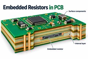
You may also like