MOSFET pinout identifies which physical connections belong to the gate, drain and source. These terminal names stay familiar across many devices, but their pin numbers and positions can change with the part number and package. Reading the correct view matters: a connection that appears on the left in a front view may appear on the right when the component is turned over.
For boards using MOSFETs, correct pin mapping supports both reliable connections and accurate component placement. EBest Circuit provides PCB fabrication, SMT and through-hole assembly, and DFM support for customer designs. To discuss manufacturing and assembly for your MOSFET-based board, contact sales@bestpcbs.com.
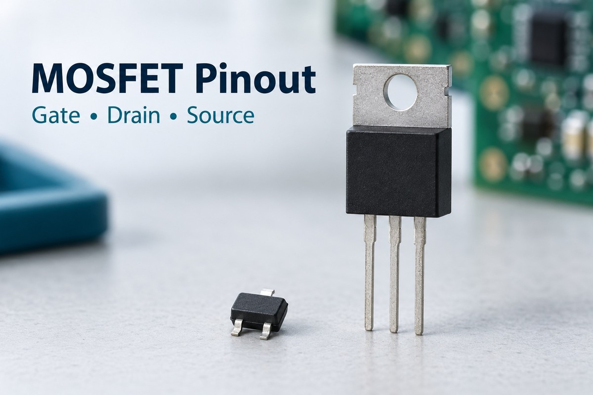
What Do the Three MOSFET Pins Do?
The gate controls the conducting channel between the drain and source. In a typical discrete MOSFET, these three terminal functions are labeled G, D and S, even when the package has more than three physical connections.
| Terminal | Function | What it means in a circuit |
|---|---|---|
| Gate (G) | Controls channel conduction through the gate-to-source voltage, VGS | The drive voltage is referenced to the source, which is not necessarily ground. |
| Drain (D) | One end of the controlled current path | Its connection must match the intended circuit and body-diode orientation. |
| Source (S) | The other end of the controlled current path and the reference for VGS | Source voltage determines the gate voltage needed to control the channel. |
For an enhancement-mode N-channel MOSFET, a sufficiently positive gate-to-source voltage turns the channel on. For an enhancement-mode P-channel device, the required polarity is negative. The threshold voltage marks the start of conduction under specified test conditions; it is not the voltage that guarantees low on-resistance.
The insulated gate behaves capacitively. It needs charging and discharging during switching, even though steady-state gate current is very small. This also explains why a floating gate can produce confusing multimeter readings.
Terminal names and pin numbers describe different things. “Gate” describes an electrical function; “pin 1” identifies a physical connection in a particular package drawing. Pin 1 is not universally the gate.
How to Read a MOSFET Pinout Diagram
A MOSFET pinout diagram becomes useful only when its viewing direction matches the way you are looking at the component. Begin with the full part number and package variant, then read the view label and pin numbering together.
- Front view: Often used for upright through-hole packages. Follow the drawing’s indicated face and lead direction before interpreting left-to-right order.
- Top view: Looks down onto the component body. Pin 1 may be identified by a dot, chamfer or another feature defined in the package drawing.
- Bottom view: Looks toward the underside or solder connections. Copying this arrangement directly into a top-view sketch can reverse the apparent positions.
Match numbered connections to the pin-function table rather than inferring their functions from the outline alone. A schematic symbol shows electrical relationships; its visual arrangement does not establish the physical pin order.
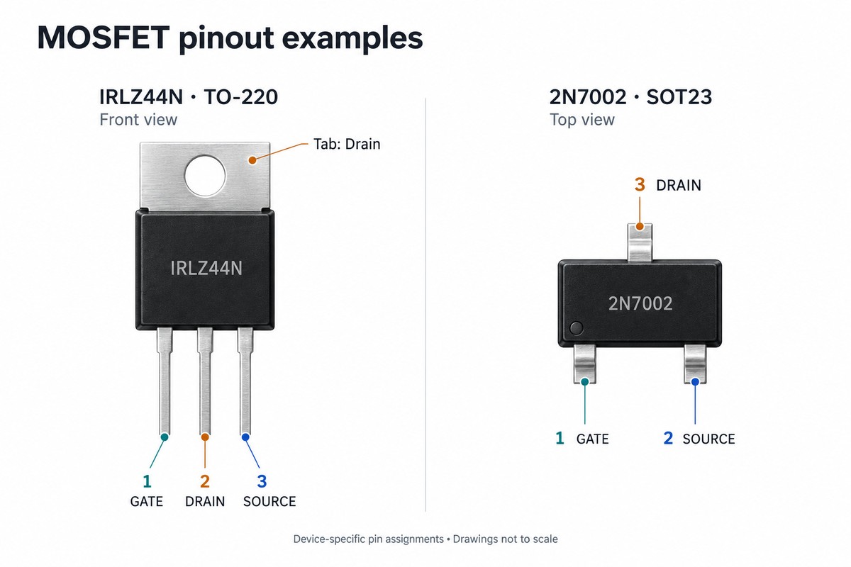
For example, the IRLZ44N in its TO-220 package has pin assignments 1 = Gate, 2 = Drain and 3 = Source. That numbered assignment remains the same when you rotate the device, but the apparent left-to-right order changes. Remembering “G-D-S” without remembering the viewing direction loses essential information.
The pin diagram and recommended PCB land pattern also serve different purposes. The first identifies connections; the second describes the copper pads used to mount the package. Both are needed when translating the component into a PCB footprint.
MOSFET Pin Configuration in Common Packages
Package size and shape do not define one universal MOSFET pin configuration. The following examples show why the exact device matters.
| Device and manufacturer | Package | Connection assignment |
|---|---|---|
| IRLZ44N, Infineon | TO-220 | Pin 1 = G; pin 2 = D; pin 3 = S; metal tab = D |
| 2N7002, Nexperia | SOT23 | Pin 1 = G; pin 2 = S; pin 3 = D |
| CSD17302Q5A, Texas Instruments | SON, 5 mm × 6 mm | Pins 1–3 = S; pin 4 = G; pins 5–8 = D; exposed pad = D |
The two three-lead examples already show a key difference: pin 2 is the drain on the IRLZ44N, but the source on the 2N7002. Applying a familiar three-pin sequence to a different device can therefore swap its power connections.
A small SOT23 device also cannot be read as a straight row of three pins: two leads sit on one side and the third sits opposite them. Its outline and numbering must be interpreted together.
In a leadless power package, some connections lie underneath the body. A top photograph alone cannot show the complete solder interface. The exposed pad may carry an electrical connection as well as conduct heat, so treating it as an electrically neutral heatsink area can create a PCB error.
These examples are specific device assignments, not rules for every TO-220, SOT23 or SON MOSFET. Likewise, an eight-pin package can contain one transistor or multiple transistors, depending on the part number.
Why Do Some MOSFETs Have More Than Three Pins?
More physical pins do not necessarily mean more independently controlled terminals. Power MOSFET packages often provide several connections to the same source or drain, creating parallel paths between the die and the PCB. Larger metal connections also help conduct heat away from the device.
An exposed pad is another physical connection that may share a source or drain net. Its electrical identity comes from the device’s pin information, not from its size or central position.
Some four-pin power MOSFETs have a Kelvin source connection. This provides a separate source reference for the gate driver, while the main source lead carries load current. Separating these paths reduces the influence of voltage developed across the shared source inductance during rapid current changes. Although both connections reach the source internally, their PCB routing serves different purposes.
The body, or bulk, terminal is a separate concept. MOSFET device theory describes gate, drain, source and body; many discrete devices connect body to source internally. A four-pin Kelvin-source package should therefore not be assumed to expose an independent body terminal.
How to Identify MOSFET Pins with a Multimeter
A multimeter can help distinguish terminals on a suitable discrete MOSFET, but it cannot reliably identify every unknown package. The method below applies to a conventional, isolated, enhancement-mode silicon MOSFET with an intrinsic body diode. Integrated protection, multiple transistors and unusual internal connections can change the readings.
Prepare the device. Disconnect power, discharge stored energy and isolate the component from other circuit paths. Use ESD precautions and a meter whose test voltage is suitable for the device. Confirm the meter’s probe polarity in diode mode.
Locate the likely gate. On a device without internal gate-protection paths, the gate should show very high resistance to both remaining terminals in either polarity, after charging effects settle. This is an identification clue, not proof: protection structures and damage can produce different results.
Identify the drain-source diode direction. Once a likely gate is identified, keep it connected to the candidate source so that VGS remains zero during each diode test. For a known channel type, the expected forward direction is:
| Channel type | Positive probe | Negative probe | Expected indication with channel off |
|---|---|---|---|
| N-channel | Source | Drain | Forward body-diode reading |
| P-channel | Drain | Source | Forward body-diode reading |
With the probes reversed, the device should normally block at the meter’s test voltage. The forward reading varies with the device, temperature and meter test current; one fixed voltage is not a universal pass criterion.
If the channel type is unknown, diode direction alone cannot uniquely establish both the channel type and the source/drain labels. Part markings and the corresponding datasheet remain important.
Account for gate charge and surrounding circuitry. A meter can charge the gate and turn the channel on, causing conduction that obscures the body-diode result. Gate-to-source discharge removes that stored charge on an isolated enhancement-mode device. On an assembled board, resistors, drivers and parallel semiconductors may create additional current paths.
These measurements support identification and basic troubleshooting. They do not establish rated-voltage performance, switching behavior or on-resistance under operating load.
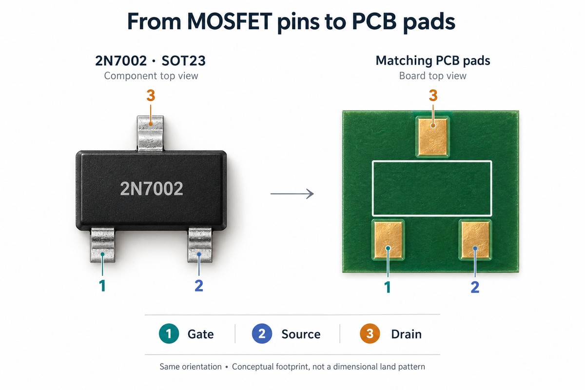
How MOSFET Pin Numbers Map to PCB Footprint Pads
A PCB connects a MOSFET correctly when the schematic pin numbers correspond to the physical terminal numbers represented by the footprint pads. Matching the package dimensions alone is insufficient.
For the Nexperia 2N7002 example, the mapping is:
| Schematic terminal | Device pin | Corresponding footprint pad |
|---|---|---|
| Gate | 1 | 1 |
| Source | 2 | 2 |
| Drain | 3 | 3 |
If a symbol instead assigns drain to pin 2 and source to pin 3, the device may still fit the footprint perfectly. The board can even pass connectivity checks against that incorrect library mapping, yet connect the transistor incorrectly. This is why a footprint’s name or 3D appearance cannot establish electrical compatibility.
For packages with repeated source or drain terminals, every required connection must reach the intended net. The exposed pad must also have the correct electrical assignment. CAD libraries may represent shared connections differently, but the resulting physical connections must agree with the device.
Orientation is equally important during assembly. The footprint’s pin-1 reference, component placement rotation and actual package marking need to describe the same orientation. An otherwise correct pad mapping will not compensate for a rotated component.
FAQs About MOSFET Pinout
Can the drain and source be swapped?
Not as a general replacement rule. An enhanced channel can conduct in either direction under suitable conditions, but the body diode and gate-to-source reference make drain and source behave differently in a circuit. Reverse channel conduction does not make the pins interchangeable.
Do N-channel and P-channel MOSFETs always have different pin orders?
No. Channel type describes electrical behavior, not a mandatory package pin order. Two devices may share the same arrangement while requiring opposite gate-drive polarity.
Is a MOSFET source always connected to ground?
No. That is common in an N-channel low-side switch, but the source can sit at another voltage in other circuit arrangements. Gate drive is determined relative to the source.
Can a short SMD marking uniquely identify a MOSFET?
Not always. Short codes can be reused across manufacturers or device families. Package dimensions, manufacturer identification and the complete marking help distinguish possible matches.
Does a matching pinout make two MOSFETs interchangeable?
No. Voltage rating, gate-drive requirements, on-resistance, switching characteristics, thermal behavior and package dimensions must also suit the circuit. Matching pins establish only part of the compatibility.
For PCB fabrication and assembly of your MOSFET-based design, contact EBest Circuit at sales@bestpcbs.com to discuss the board, package and MOSFET pinout requirements.