





An SSOP package, or Shrink Small Outline Package, is a surface-mount IC package with gull-wing leads on two sides. It gives designers a compact, leaded package whose solder joints remain visible around the body.
SSOP is a package family, not one fixed mechanical outline. Two parts described as SSOP may use different body widths, lead spans, pitches, heights, and PCB land patterns, so the exact package code and manufacturer’s drawing must guide footprint design and assembly.
What Is SSOP Package?
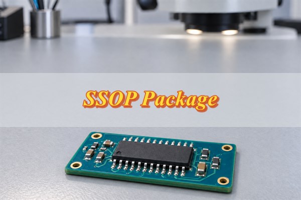
SSOP stands for Shrink Small Outline Package, a compact surface-mount IC package with gull-wing leads arranged along two opposite sides. Compared with a standard SOIC of similar pin count, an SSOP generally uses a narrower body and finer lead spacing, reducing PCB area while keeping the solder joints exposed for optical inspection and rework.
SSOP describes a package family rather than one interchangeable outline. Confirm the exact manufacturer’s package code and drawing before choosing a PCB footprint because body width, lead pitch, overall span, height, and land-pattern requirements can differ. The practical tradeoff is greater board density with less assembly margin, so stencil design, placement accuracy, and solder-bridge control need closer attention.
What Are the Standard SSOP Package Dimensions?
There is no single set of SSOP package dimensions for every device. The same SSOP label covers multiple JEDEC outlines, body widths, heights, lead counts, and pitches. Use the package code on the exact component datasheet before selecting or creating a footprint.
The examples below from the NXP SSOP package index show how dimensions can vary within one manufacturer’s package family. The body column reports package length × body width × the height value listed by NXP, which may be nominal or maximum depending on the outline.
| Package Example | Pitch | Body (mm) |
| SSOP16, SOT338-1 | 0.65 mm | 6.2 × 5.3 × 2.0 |
| SSOP20, SOT339-1 | 0.65 mm | 7.2 × 5.3 × 2.0 |
| SSOP24, SOT340-1 | 0.65 mm | 8.2 × 5.3 × 2.0 |
| SSOP28, SOT341-1 | 0.65 mm | 10.2 × 5.3 × 2.0 |
| SSOP16, SOT519-1 | 0.635 mm | 4.9 × 3.9 × 1.73 |
| SSOP48, SOT370-1 | 0.635 mm | 15.9 × 7.5 × 2.8 |
These examples explain why SSOP-16 package dimensions or SSOP-20 package dimensions cannot be inferred from pin count alone. A 16-pin SSOP package can belong to a 5.3 mm-wide, 0.65 mm family or a 3.9 mm-wide, 0.635 mm family. Likewise, an SSOP-28 package should be checked by its package drawing rather than by an unqualified library name.
What Lead Pitch Does an SSOP Package Use?
A 0.65 mm lead pitch is common, but it is not universal. Official manufacturer package libraries also list 0.635 mm and 0.64 mm SSOP families, so the pitch must come from the exact package drawing or orderable-part datasheet.
Pitch is the center-to-center distance between adjacent leads. It controls pad spacing, solder-mask geometry, routing escape, stencil behavior, placement tolerance, and the optical resolution needed to detect bridges. Do not assume that a 0.65 mm footprint is compatible with a 0.635 mm package because the difference looks small; the offset accumulates across the lead row.
Confirm the pitch together with body width, lead count, overall lead span, lead width, lead length, and package height. Use that complete set of dimensions, not the pitch alone, to choose or build the PCB land pattern.
How Should You Design an SSOP PCB Footprint?
Build or select the footprint from the exact package code and its recommended land pattern. Component lead dimensions describe the part; they are not the same as the PCB pad dimensions needed to solder it.
- Confirm the exact package code: Start with the manufacturer’s part number, package suffix, pin count, and drawing code. A library name such as “SSOP-20” is not specific enough on its own.
- Check pitch and lead geometry: Read the specified pitch and the dimensional limits for lead width and length, body width and length, overall lead span, standoff, and coplanarity. A nominal body size alone does not show where every lead can land.
- Use the recommended land pattern: Prefer the component manufacturer’s current recommendation when one is available. For example, TI’s DB0028A drawing shows 0.45 × 1.85 mm lands on 0.65 mm pitch for that specific 28-lead outline, not for every SSOP-28 package.
- Check solder mask and paste openings: Confirm that the fabricator can hold the intended mask web and that stencil apertures suit the paste and assembly process. Excess paste can increase bridging, while too little paste can produce opens or weak joints.
- Verify pin 1 and component orientation: Align the footprint marker, silkscreen, courtyard, centroid rotation, and assembly drawing. Leave enough access around both lead rows for optical inspection and rework.
Never assume that two SSOP devices with the same pin count can share a footprint. Compare the complete drawing and recommended land pattern before reusing a library part.
What Is the Difference Between SOIC and SSOP Packages?
SSOP is usually the better choice when board area is tight, while SOIC generally offers more assembly and rework margin. The table compares the points that most often affect package selection; exact dimensions and performance still depend on the orderable device and its package drawing.
| What Users Care About | SOIC | SSOP |
|---|---|---|
| PCB area | Usually needs more board area for a similar lead count | Usually uses less board area for a similar lead count |
| Common lead pitch | Often 1.27 mm | Often 0.65, 0.635, or 0.64 mm |
| Assembly margin | Wider lead spacing gives more print and placement margin | Tighter spacing needs closer stencil, placement, and reflow control |
| Prototyping and hand soldering | Generally easier to place and solder manually | Feasible with suitable tools, magnification, and operator control |
| Inspection and rework | Exposed leads are easier to see and access | Exposed leads remain visible, but tighter spacing makes bridges and rework more demanding |
| Footprint compatibility | Not interchangeable with SSOP without checking the exact drawing and land pattern | Needs its own checked land pattern rather than an assumed SOIC footprint |
SOIC is often easier to prototype, inspect, and rework when board area is available. SSOP is useful when density matters and the assembly process can control the finer pitch. Neither is a drop-in substitute for the other, even when the pin count and electrical function appear to match. The SOIC package guide provides additional SOIC-specific detail.
What Is the Difference Between SSOP and TSSOP Packages?
TSSOP is a thinner small-outline package family and is often more compact than a comparable SSOP, but the names alone do not prove footprint compatibility. In TI’s 20-pin package comparison, the DB SSOP has a 2.00 mm maximum height, while the PW TSSOP has a 1.20 mm maximum and occupies less footprint area. That example illustrates the family difference; it does not define every SSOP or TSSOP.
Pitch is not a reliable shortcut because both families contain multiple outlines. NXP listings, for example, include TSSOP packages at 0.65 mm and 0.5 mm pitch, while its SSOP listings include 0.65 mm and 0.635 mm examples. Before changing packages, compare pitch, body width and length, lead span, lead dimensions, height, pinout, and the recommended land pattern from the exact device drawings.
The same pin count or device family does not make an SSOP and TSSOP mechanically interchangeable. Treat a package change as a PCB footprint check, not as a name-based substitution.
Where Are SSOP Packages Commonly Used?
SSOP packages are common where a dual-row leaded IC must fit into limited board space while keeping its joints optically accessible. The package appears across many device classes; it is not tied to a single circuit function.
- Logic and I/O: Buffers, latches, bus-interface devices, and I/O expanders are often offered in this compact leaded format.
- Data conversion: ADCs, DACs, and mixed-signal ICs may use SSOP when the layout needs moderate pin density and visible leads.
- Interfaces and communications: Transceivers, line drivers, and serial-interface devices are common candidates when routing space is limited but optical inspection still matters.
- Analog and control: Op-amps, sensor interfaces, controllers, and clock devices are available in SSOP options when their pin count and thermal needs fit the outline.
- Compact equipment: Industrial controls, consumer electronics, audio/video products, and communication hardware use SSOP when the smaller mounting area justifies the finer-pitch assembly process.
In practice, the exact device and mechanical outline should drive the decision. An application label by itself is not a reason to choose SSOP.
What Should You Consider When Selecting an SSOP Package?
Select the electrical device first, then verify that its exact SSOP option fits the board, assembly process, inspection plan, and supply strategy. Package size cannot compensate for an incorrect function, rating, or lifecycle choice.
- Does the IC meet the electrical requirement? Confirm function, pinout, ratings, speed, accuracy, interfaces, temperature range, and any thermal limits for the real board conditions.
- Does the exact outline fit the available PCB space? Check the package suffix, lead count, body size, lead span, height, courtyard, and routing access rather than comparing body width alone.
- Can the PCB and SMT process handle the pitch? Match the pad, mask, stencil, placement, and reflow requirements to the fabricator and assembler’s capabilities.
- Can the package be inspected and reworked? Allow optical access to both lead rows and enough surrounding space for the planned inspection and rework tools.
- Will the exact package remain available? Check the component’s lifecycle, authorized supply options, and qualified alternatives early enough to avoid a late footprint change.
How Is an SSOP Package Soldered to a PCB?
Production SSOP assembly normally uses solder-paste printing, pick-and-place, controlled reflow, and inspection. Fine lead spacing makes print volume and lead-to-pad alignment more sensitive than they are for a wider-pitch package, but there is no universal SSOP temperature profile.
- Print the solder paste: Align the stencil apertures with the pads and control deposit volume. Too much paste raises bridge risk; missing or incomplete deposits raise open-joint risk.
- Place the component: Match pin 1 and align both lead rows with their pads. A placement offset can push one row toward bridging while leaving too little overlap on the other.
- Reflow the assembly: Set the profile from the solder alloy and paste guidance, PCB thermal mass, and the component’s temperature limit. Board construction and nearby components change heating behavior, so a package name cannot supply one universal profile.
- Inspect the joints: After reflow, check the exposed gull-wing leads for bridging, opens, misalignment, lifted leads, and poor wetting, then use electrical testing where product risk and test access justify it.
Footprint dimensions, package and board tolerances, placement accuracy, flatness, solder paste, and stencil behavior work together. A correct package drawing cannot compensate for the wrong land pattern or a shifted paste print.
What Assembly Problems Can Occur With SSOP Packages?
The most common SSOP assembly problems are bridges, opens, misalignment, lifted leads, poor wetting, and orientation errors. Start with what is visible, then check the process condition most likely to have produced it.
| Observation | Likely Cause | First Check |
| Solder bridge | Excess or shifted paste, placement offset, pad or mask mismatch | Paste deposits, stencil apertures, placement image, and pad spacing |
| Open or low-solder joint | Missing paste, poor transfer, bent lead, coplanarity error, or weak wetting | Paste deposit, lead plane, pad finish, profile, and visible wetting |
| Component skew | Unequal deposits, placement error, or asymmetric reflow forces | Pad symmetry, deposit balance, and pre-reflow placement |
| Lifted lead | Lead damage, poor coplanarity, handling stress, or pad-height variation | Incoming lead condition, seating plane, board flatness, and local joint gap |
| Poor wetting | Oxidation, contamination, unsuitable profile, or expired/incorrect material | Lead and pad finish, paste condition, cleanliness, and reflow profile |
| Wrong orientation | Ambiguous marking or inconsistent library, CPL, feeder, and drawing data | Pin 1 on the part, footprint, placement data, and AOI model |
Do not repair the symptom before confirming the cause. Removing a bridge may restore continuity on one board, but a shifted stencil or incorrect footprint can repeat the same defect across the lot.
How Should SSOP Solder Joints Be Inspected?
Inspect SSOP joints with visual or automated optical methods first because the gull-wing leads and fillets are exposed. Judge the joints against the applicable product requirement and assembly standard rather than a generic online photograph.
- Confirm identity and orientation: Verify the part marking, package suffix, pin 1, polarity where applicable, and seating position before judging individual joints.
- Inspect the lead rows: Check lead-to-pad alignment, unintended connections, insufficient solder, lifted or damaged leads, visible wetting, and consistent fillet formation at the toe and heel regions that can be seen.
- Use AOI for repeatable coverage: Program the correct package geometry and joint criteria. AOI can compare every visible lead quickly, but lighting, library setup, board contrast, and obstructions affect its results.
- Apply X-ray only when justified: X-ray is not automatically required for an ordinary exposed-lead SSOP joint. Use it when a hidden feature, overlapping structure, adjacent bottom-terminated device, or failure investigation cannot be resolved optically.
- Add electrical testing where needed: Continuity, shorts, in-circuit, or functional testing can reveal failures that appearance alone cannot prove. Electrical testing complements solder-joint inspection; it does not replace it.
IPC-A-610 is widely used for electronic-assembly acceptance, but the applicable revision and class must come from the product or customer requirement. Do not infer pass limits from a photograph.
FAQs About SSOP Packaging
Q1: What do codes such as DB and DBQ mean on an SSOP listing?
A1: They are manufacturer-specific package designators, not interchangeable names for one outline. For example, two SSOP codes can indicate different body widths or lead pitches. Match the code on the orderable part number to the drawing in the same datasheet.
Q2: Can an SSOP IC plug directly into a solderless breadboard?
A2: No. SSOP is a surface-mount package, and its fine lead spacing does not match a standard 2.54 mm breadboard grid. For prototyping, solder the IC to a suitable SSOP-to-DIP adapter or use a purpose-built carrier board.
Q3: What should you check before buying an SSOP-to-DIP adapter?
A3: Match the adapter to the exact pin count, lead pitch, body width, lead span, pad layout, and pin 1 orientation. A board labeled only “SSOP-16” may not fit every 16-lead SSOP outline.
Q4: Does the SSOP name guarantee RoHS compliance?
A4: No. SSOP describes the package family, not the terminal finish or environmental status. Check the exact orderable part number, material declaration, and applicable compliance documentation.
Q5: How should moisture-sensitive SSOP parts be stored before reflow?
A5: Follow the moisture-sensitivity label and the component manufacturer’s handling instructions. Keep unopened parts in their specified moisture-barrier packaging. After opening the bag, observe the stated floor life and use controlled dry storage or baking only when the product instructions and applicable J-STD-033 requirements call for it.
Conclusion
The safest SSOP design starts with the exact orderable part, not a generic library name. Before PCB layout, confirm its pitch, body dimensions, lead geometry, package code, and recommended land pattern. That work gives printing, placement, soldering, and inspection a sound starting point.
If your PCB uses SSOP or another fine-pitch SMT package, send the part number, datasheet, PCB files, BOM, quantity, and assembly requirements to sales@bestpcbs.com for review and quotation.
You may also like







Tags: pcb footprint, SMT assembly, solder joint inspection, SSOP Package