Top robotics 3D vision illuminator PCB manufacturers in Germany support lighting hardware that helps cameras capture stable depth data on reflective, dark, textured, or fast-moving objects. Choosing a supplier is not simply a matter of finding a company that can produce an aluminum PCB: the board must carry the LED load, remove heat, preserve optical consistency, fit the mechanical assembly, and arrive in time for camera and robot validation.
This guide helps German buyers assess manufacturers, prices, lead times, thermal capabilities, and sourcing routes for an illuminator PCB project. Buyers who also need a China manufacturing option can work with EBest Circuit, founded in 2006 and supported by 160 employees, more than 20 years of PCB and PCBA experience, 1,800+ customers across 40 countries, and a reported 97% on-time delivery rate. Its service combines PCB fabrication, component sourcing, PCBA, and testing. Send your Gerber files, BOM, target quantity, and required delivery date to sales@bestpcbs.com for an initial engineering review.
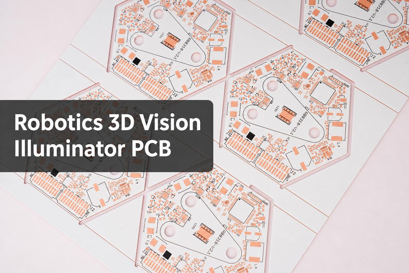
What Is a Robotics 3D Vision Illuminator PCB?
A 3D vision illuminator PCB is the circuit board that supports and drives the light source used by a robotic vision system. Depending on the sensing method, the illuminator may project infrared flood light, a structured pattern, a line, or synchronized pulses. The camera records the reflected light so that the vision system can calculate depth, locate parts, inspect surfaces, or guide a robot.
The PCB may look simple because LEDs dominate the visible side of the assembly, but its performance affects the complete optical system. Uneven LED current can create inconsistent brightness. Poor heat spreading can shift wavelength, reduce light output, shorten LED life, or distort calibration. Mechanical error can move the emitting surface away from the intended optical axis.
A buyer should therefore define the illuminator as an electro-optical assembly rather than as a generic LED board. Important inputs include:
- illumination wavelength and optical power;
- continuous, strobed, or pulsed operating mode;
- LED quantity, package, current, and forward voltage;
- required thermal resistance and maximum junction temperature;
- board outline, mounting holes, connector position, and height restrictions;
- driver topology, synchronization signals, and protection circuits;
- camera distance, field of view, enclosure, lens, diffuser, or projector interface;
- operating temperature, vibration, contamination, and service-life targets.
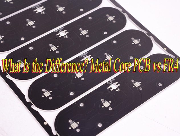
MCPCB is often suitable when the main challenge is removing heat from a compact LED array. A more complex illuminator may instead need a multilayer FR-4 board, a hybrid construction, or separate LED and control boards. The correct choice depends on the thermal path, signal requirements, component density, and mechanical design.
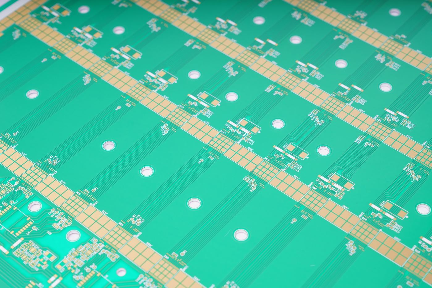
Top 3D Vision Illuminator PCB Manufacturers in Germany
The following companies are worth evaluating for thermal, high-reliability, prototype, or advanced PCB requirements in Germany. Their available services fit parts of an illuminator PCB project, but buyers should still confirm the MCPCB construction, PCBA scope, optical testing, available capacity, and production location for each quotation.
CONTAG AG, Berlin: CONTAG manufactures IMS and metal-core PCBs for LED, industrial, automotive, energy, and other thermally demanding applications. It also offers multilayer, HDI-SBU, high-frequency, flex, and rigid-flex boards. It is a strong candidate when an illuminator requires thermal engineering support, a fast German prototype, or a hybrid solution rather than a basic one-layer aluminum board.
Unimicron Germany GmbH, Geldern: Unimicron Germany offers multilayer boards up to 24 layers, HDI, high-frequency technology, metal-inlay solutions, IMS/heatsink technology, and other heat-management options. The company serves industrial and robotics applications, making it relevant when an illuminator combines power, control, communication, and thermal functions.
Becker & Müller Schaltungsdruck GmbH, Steinach: Becker & Müller provides in-house German production for prototypes and small batches and keeps IMS, FR-4, high-Tg, HF, and flex materials in stock. Its express service covers one- and two-sided boards, multilayers, and rigid-flex products. Buyers should ask which delivery option applies to the selected IMS material and stack-up.
Hotoprint Elektronik: Hotoprint manufactures PCBs in Germany, including multilayers up to 12 layers, flexible, rigid-flex, semiflex, and aluminum boards. Prototype and express services can begin from three working days, although the actual delivery date depends on the final MCPCB specification.
Leiton GmbH, Berlin: Leiton offers aluminum and copper IMS boards, German prototype production, an online calculator, and custom quotation support. Its Copper-IMS guide lists different lead-time options by layer count and shows which constructions require a direct enquiry.
This shortlist should begin a technical comparison, not end it. Some German companies focus mainly on bare PCBs, while a robotics buyer may need component sourcing, LED bin management, SMT assembly, programming, and functional testing. Ask each supplier to state exactly which operations are included and where they will be performed.
3D Vision Illuminator PCB Prices in Germany: What Buyers Should Compare
There is no reliable standard market price for a custom 3D vision illuminator PCB. Two boards with the same outline can have very different costs because price depends on material, panel utilization, copper weight, thermal dielectric, layer count, surface finish, tolerances, testing, quantity, and delivery speed.
For MCPCB prototypes, the main price drivers normally include:
- aluminum versus copper base;
- standard versus high-performance thermal dielectric;
- one-layer, two-layer, or multilayer IMS construction;
- board thickness and copper weight;
- routed outline, slots, countersinks, or tight mechanical tolerances;
- white solder mask, special marking, ENIG, or another nonstandard finish;
- electrical test, documentation, and expedited manufacturing;
- assembly quantity, LED package, placement density, and test coverage.
The lowest bare-board price is not always the lowest project cost. A cheaper board can become expensive if it needs a separate assembler, additional incoming inspection, repeated engineering communication, or rework after thermal testing. Conversely, paying a German prototype premium may be justified when local engineering contact or a very short iteration loop prevents a delayed robot trial.
Request quotations with the same manufacturing package and commercial assumptions. Each RFQ should specify quantity, panelization responsibility, material, copper, surface finish, test scope, tooling, delivery term, destination, and whether freight and tax are included. If PCBA is required, compare the BOM price, approved component sources, alternates, setup charges, programming, functional testing, and packaging separately.
A practical comparison uses at least three totals: prototype cost, landed cost, and cost of the next production quantity. This prevents an attractive sample price from hiding an unsuitable scale-up model.
What Lead Times Do German Manufacturers Offer for 3D Vision Illuminator MCPCBs?
German manufacturers publish useful benchmarks, but buyers must distinguish manufacturing time from delivery to the project site. The clock may begin only after data approval, material confirmation, DFM closure, and order release.
Leiton’s Copper-IMS technology document dated May 26, 2025, provides the clearest layer-specific public reference:
| Copper-IMS construction | Online calculation | Standard on explicit enquiry |
|---|---|---|
| 1 layer | 12 working days | 5 working days |
| 2 layers | Not available | From 4 working days |
| 4-6 layers | Not available | From 5 working days |
These are Leiton’s manufacturing options for Copper-IMS boards. They are not universal German market lead times and do not automatically include assembly or shipping.
Eurocircuits lists five working days for bare boards and ten working days for assembled boards in its one-layer aluminum IMS pool. Because its PCB and assembly services are handled by factories in Germany and Hungary, buyers who require production specifically in Germany should confirm the assigned plant.
For project planning, separate the schedule into five parts:
- DFM review and clarification;
- special-material or component procurement;
- bare-board fabrication;
- assembly, programming, and functional testing;
- packing and transport to the German destination.
An advertised four- or five-day build does not help if a selected LED has a six-week procurement lead time. Send the complete BOM and approved-alternate policy early, and ask the supplier to state the ready-to-ship date rather than only the fabrication cycle.
Germany vs China for Robotics 3D Vision Illuminator PCB Manufacturing
Germany and China should not be compared through a single price or speed claim. The better choice depends on the development stage, specification stability, order quantity, communication needs, supply chain, and required manufacturing scope.
| Buyer priority | Germany | China |
|---|---|---|
| Local iteration | Strong fit | Remote review required |
| Integrated PCBA | Supplier-dependent | Commonly available |
| Repeat-volume cost | Quote-dependent | Often competitive |
| Transport | Shorter regional route | Add freight and customs |
| Best use | Urgent local prototypes | Integrated builds and scaling |
A sensible sourcing strategy may use German manufacturing for an urgent local iteration and an approved China partner for integrated PCBA or repeat volume. Compare both options using the same material, stack-up, tolerances, surface finish, inspection scope, Incoterm, and delivery destination. If two sources will be used, approve the same golden sample before transfer.
Which MCPCB Process Capabilities Does EBest Circuit Offer for Robotics 3D Vision Illuminators?
For illuminator projects, EBest Circuit supports the following metal-base PCB production ranges:
| Item | Standard capability | Special capability |
|---|---|---|
| Thermal conductivity | 1-3 W/(m·K) | 3-8 W/(m·K), subject to material confirmation |
| Board construction | Single-sided, double-sided, single-sided two-circuit-layer aluminum/copper base | Single-sided four-layer, subject to review |
| Thermoelectric separation | Copper-base PCB | Copper-aluminum composite construction |
| Inner-layer copper | 0.5-3 oz | 4 oz or above, subject to review |
| Outer-layer copper | 1-3 oz | Above 3 oz, subject to review |
| Processing thickness | 0.8-3.0 mm | 4.0 or 5.0 mm by material order; bendable aluminum: 0.4-1.0 mm |
| Maximum aluminum-board size | 480 × 1180 mm | Single-sided aluminum: 1600 × 480 mm |
Final capability depends on the complete files, material availability, and quantity.
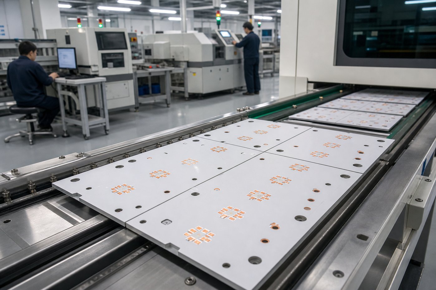
What Lead Times Does EBest Circuit Offer for Robotics 3D Vision Illuminator PCBs?
For standard MCPCB prototypes below one square meter, buyers can use the following fabrication times as an initial planning reference. The confirmed schedule depends on the released specification and current capacity.
| MCPCB layers | Normal service | Fastest service |
|---|---|---|
| 1 layer | 4 days | 24 hours |
| 2 layers | 14 days | 168 hours |
| 4 layers | 21 days | Confirm before ordering |
These timings apply to standard MCPCB prototypes with a total order area below one square meter. The standard specification uses conventional aluminum material, 0.8-2.0 mm board thickness, 0.5 oz or 2 oz copper, lead-free HASL, white solder mask, black silkscreen, and nominal thermal conductivity of 0.8 W/(m·K).
High-conductivity materials, thermoelectric-separation copper-base PCBs, OSP, special copper weights, unusual thicknesses, tight tolerances, and nonstandard panel requirements need a project-specific schedule. Production timing begins after the manufacturing data, material choice, technical questions, and commercial terms are confirmed.
The table covers bare-board production only. Component purchasing, PCBA, functional testing, packing, international freight, customs clearance, and delivery within Germany must be added separately. If the project deadline is fixed, send the files and required arrival date to sales@bestpcbs.com so EBest Circuit can check current capacity and provide a realistic ready-to-ship schedule.
EBest Circuit Engineering Case: Building a Robotics 3D Vision Illuminator PCB
In a robotics 3D vision system, the illuminator must project repeatable light while the camera captures depth information. If heat builds up unevenly beneath the LED array, brightness can drift across the field of view and make optical calibration less stable. The PCB therefore acts as part of the lighting system, not just as a carrier for LEDs.
For one German illuminator project, EBest Circuit manufactured 180 pieces of a single-sided, two-circuit-layer thermoelectric-separation copper-base PCB. Its direct thermal path moved heat from the LED mounting area into the 1.5 mm copper base, while the isolated circuit layer carried power to the emitters. The specified 3 W/(m·K) material and 1 oz / 1 oz copper were selected to balance heat removal, current distribution, and the required 1.6 mm ±10% finished thickness.
The confirmed production specification was:
- 1.5 mm copper base;
- 1 oz / 1 oz copper;
- thermal conductivity of 3 W/(m·K);
- finished board thickness of 1.6 mm ±10%;
- white solder mask and black silkscreen;
- OSP surface finish;
- delivery according to the customer’s panel drawing, with each individual board retaining its specified process rails.
White solder mask kept the LED side visually clean, black legend made polarity and assembly marks easy to identify, and OSP provided a flat surface for LED soldering. The boards were delivered in the customer’s released panel format with the required process rails, allowing the panels to enter LED assembly without repanelization.
Before production, the customer approved the final board configuration and panel format. The completed 180-piece lot was supplied with the requested COC and electrical test report. The German team therefore received one consistent board build for LED assembly and later camera-and-illuminator validation, without having to reconcile different thermal, mechanical, and panel specifications after delivery.
Why Choose EBest Circuit for 3D Vision Illuminator PCB Manufacturing?
EBest Circuit is a China-based PCB and PCBA manufacturing partner serving German and international buyers. Founded in 2006, the company has more than 20 years of industry experience, 160 employees, 1,800+ customers across 40 countries, and a reported 97% on-time delivery rate. It is most relevant when the project needs more than a bare-board price.
Technical support around the buyer: One sales contact is supported by three technical team members. DFM review, BOM optimization, and process-fit suggestions are available from engineers with long PCB and PCBA experience.
One project scope from board to test: PCB fabrication, component sourcing, PCBA, and customer-defined testing can be coordinated together, reducing handoffs between unrelated suppliers.
Prototype and low-volume support: Engineering samples and small batches help teams verify thermal behavior, mechanical fit, assembly, and optical performance before scaling.
Factory and supply-chain coverage: In-house PCB and PCBA resources are supported by more than 1,000 supply-chain partners, helping coordinate materials, components, quality controls, and delivery.
Traceability and quality systems: The digital workshop can trace material and product batches, production cycles, and progress. Available quality certifications include ISO 9001, ISO 13485, IATF 16949, and AS9100D.
A German manufacturer may still be preferable when physical production in Germany or immediate local iteration is mandatory. EBest Circuit is a stronger candidate when the buyer values integrated China sourcing, technical support, coordinated PCBA, traceability, and a route from prototypes to repeat production.
What Should You Send EBest Circuit for a 3D Vision Illuminator PCB Quote?
A first quotation does not need a perfect document package. To let EBest Circuit understand the project and identify missing information, start with five essentials:
- your Gerber or ODB++ data, plus the board outline;
- the LED or PCBA BOM if assembly is required;
- prototype and expected production quantities;
- known thermal targets, such as base material, conductivity, copper weight, or heatsink interface;
- the German delivery location and the date the boards or assemblies are needed.
If your files are not complete yet, that is fine. Send what you have, and the engineering team will identify the few details needed next to evaluate price, manufacturability, thermal performance, and lead time. You do not need to prepare the full production package before requesting an initial review.
Email the available files to sales@bestpcbs.com and state that the request is for a robotics 3D vision illuminator PCB. EBest Circuit will review the current design, explain any information still needed, and prepare the quotation around your actual development stage.
FAQs About Robotics 3D Vision Illuminator PCB
Should a 3D vision illuminator use an aluminum or copper-base PCB?
Aluminum MCPCB is often suitable for cost-controlled LED heat spreading. Copper-base and thermoelectric-separation constructions can provide a more direct thermal path for higher heat density or tighter thermal targets. The right choice depends on LED power, pulse conditions, dielectric performance, mechanical structure, and the heatsink interface.
Can German manufacturers provide fast MCPCB prototypes?
Yes. Some German suppliers offer express or short prototype services. Leiton lists a five-working-day option for a one-layer Copper-IMS construction by direct enquiry, while more complex constructions require confirmation. Always check when the production clock begins and whether assembly and transport are included.
What should buyers compare besides the quoted PCB price?
Compare the metal base, dielectric, thermal conductivity, copper weight, board thickness, surface finish, tolerances, electrical test, documentation, tooling, panel delivery format, freight, and tax. For PCBA, also compare component sources, assembly setup, programming, functional testing, and approved alternatives.
Does EBest Circuit manufacture thermoelectric-separation copper-base PCBs?
Yes. EBest Circuit manufactures thermoelectric-separation copper-base PCBs. One completed German customer order used a single-sided, two-circuit-layer construction with a 1.5 mm copper base, 1 oz / 1 oz copper, 3 W/(m·K) thermal conductivity, OSP, and a finished thickness of 1.6 mm ±10%.
How can a German buyer reduce risk when sourcing an illuminator PCB from China?
Release a complete manufacturing package, approve the production data before fabrication, define acceptable materials and substitutions, agree on inspection and test reports, confirm the shipping term, and approve the pilot or golden sample before repeat production. These controls make the comparison more reliable than selecting a supplier by unit price alone.
Have a robotics 3D vision illuminator PCB ready for review? Email the available files, quantity, thermal requirements, and German delivery target to sales@bestpcbs.com. EBest Circuit will check the design, clarify the key manufacturing decisions, and respond with a quotation and project-specific schedule.
You may also like



Tags: 3D vision illuminator PCB, Metal Core PCB, Robotics PCB