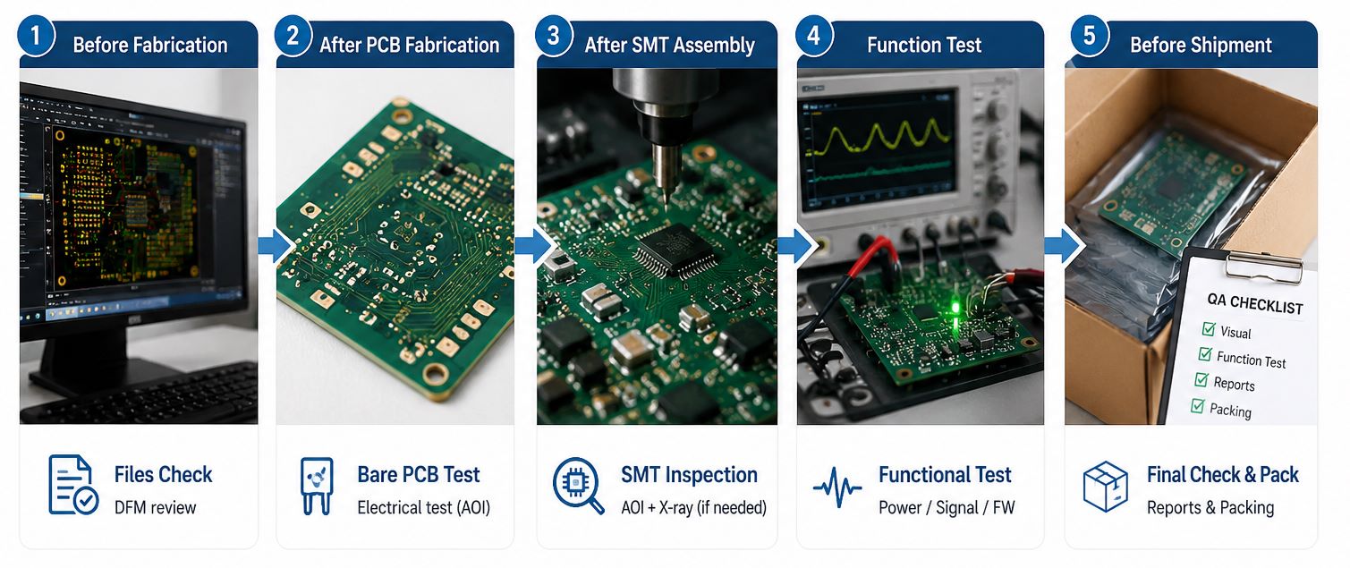
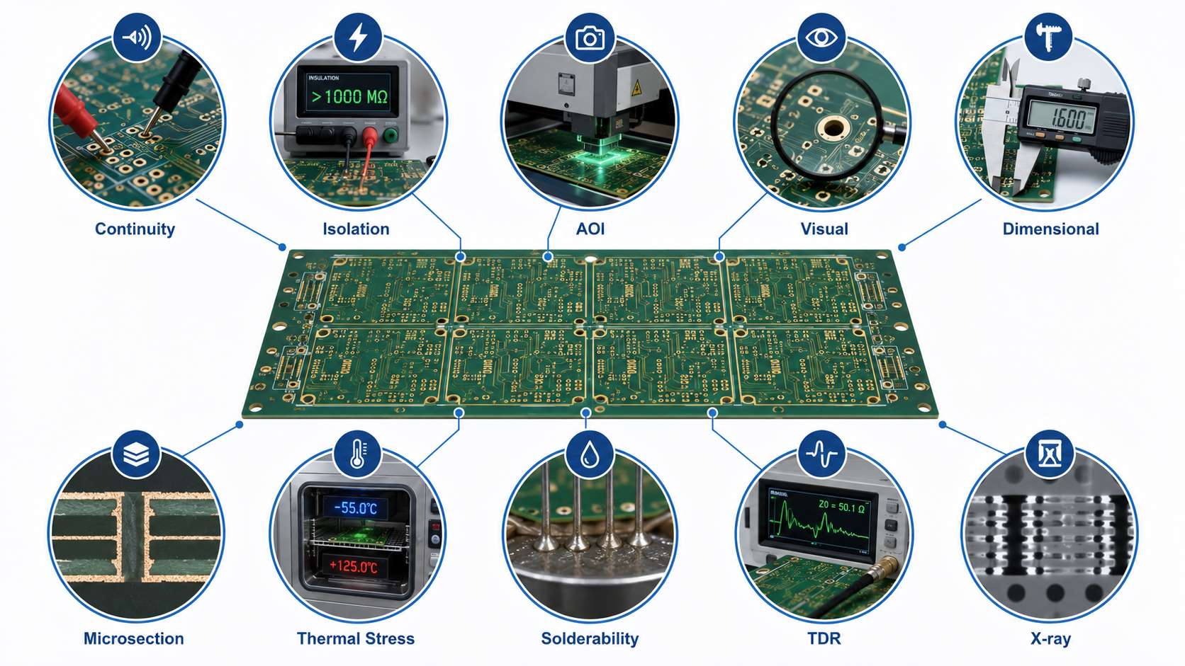
J-STD-003 addresses the solderability of bare printed circuit boards: whether the exposed surfaces intended for soldering can be wetted by molten solder. For your PCB project, that matters before components reach the assembly line. At EBest Circuit (Best Technology), we connect PCB fabrication and assembly support so that the board finish, component layout and soldering process are considered together.
What Is J-STD-003?
IPC J-STD-003 (also written IPC J STD 003 or J STD 003) is the solderability test standard for printed boards. Its subject is the board’s exposed conductors, attachment lands and plated-through holes, rather than component leads or completed solder joints.
Solderability testing helps separate a surface-wetting problem from an assembly-process problem. A satisfactory bare-board result does not prove that every joint will form correctly during production: solder paste deposition, component placement and the thermal profile remain separate parts of assembly quality.
Why Can a PCB Look Clean but Solder Poorly?
A clean-looking pad is not necessarily a readily wettable pad. Thin oxidation or contamination can interfere with the solder-to-metal interface without producing an obvious defect in an ordinary board photograph.
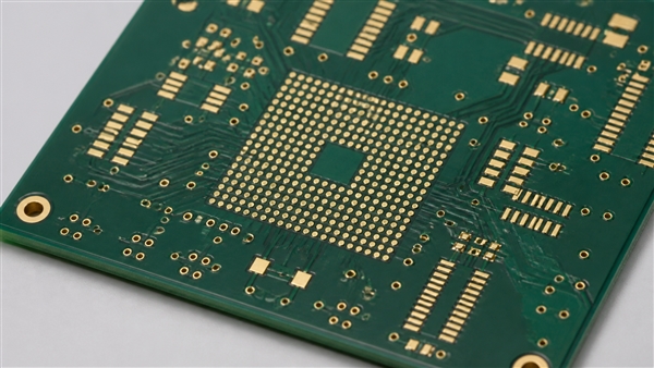
On our FR4 printed circuit boards, the solderable features include both surface-mount pads and connection points for through-hole parts. If solder withdraws from a pad, the resulting connection can be incomplete even though the copper circuit passes an electrical continuity test. Continuity and wettability answer different questions.
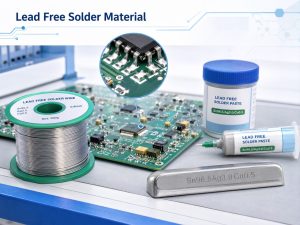
Appearance also depends on the solder alloy. Lead-free solder does not necessarily spread or look like tin-lead solder, so a comparison based only on shininess can be misleading. The important distinction is whether the intended metal surface has been wetted under the applicable test conditions.
Which Solderability Test Methods Are Used?
J-STD-003D includes visual evaluation methods and wetting-force measurement. The method must suit the board features being assessed.
Method family
Main evaluation
Edge dip
Wetting of exposed surface conductors
Surface-mount simulation
Wetting of surface-mount lands
Wave solder or solder float
Solderability of plated-through-hole features
Wetting balance
Wetting behavior recorded as force over time
For a board carrying both fine-pitch components and connectors, a surface-pad observation cannot answer every question about the holes. Likewise, a test on an unrelated reference board cannot establish the condition of your production lot. Representative material and the agreed evaluation method are essential to a useful result.
What Does a Wetting Balance Test Measure?
A wetting balance test records the force acting on a specimen as it contacts molten solder. The force-time response shows how wetting develops, adding information that a photograph taken after cooling cannot provide.
The response reflects surface tension, buoyancy and the developing solder meniscus. Test temperature, alloy, flux and specimen geometry affect the signal; curves obtained under different conditions are not automatically comparable. The illustration shows the measurement principle, not a measured result or a pass/fail limit.
For a difficult-to-solder pad, this measurement can help investigate delayed or weak wetting. It does not identify the root cause by itself, and it does not replace examination of the finish or the actual assembly process.
How Do Nonwetting and Dewetting Differ?
Nonwetting means solder has not formed the intended wetted interface. Dewetting describes solder withdrawing after initially covering an area, leaving an uneven coating. Both can reduce useful solder coverage, but they describe different behavior.
Observation
What it suggests
What it does not prove
Solder beads beside an uncovered pad
Possible nonwetting of that surface
That the PCB finish is the sole cause
Irregular solder islands after coverage recedes
Possible dewetting
A specific contamination source without further analysis
Smooth-looking solder on only part of the feature
Incomplete coverage still needs evaluation
Acceptance based on appearance alone
For an assembly defect, the PCB pad and the component termination should be distinguished. A board can have satisfactory solderability while a component lead has a separate surface problem. Adding more heat or flux without identifying the affected interface can damage the assembly rather than resolve the cause.
How Does PCB Surface Finish Affect Solderability?
The surface finish protects exposed copper and establishes the surface presented to the soldering process. ENIG, OSP, immersion silver, immersion tin and HASL use different protection systems, so the finish name alone cannot describe every assembly constraint.
Finish
Relevance to assembly
Project consideration
ENIG
Flat nickel-gold finish for component lands
Finish integrity and the planned soldering sequence
OSP
Organic protection over copper without a raised solder coating
Handling, storage and cumulative thermal exposure
Immersion silver or tin
Thin metallic protection on exposed copper
Packaging and finish-specific assembly conditions
HASL or lead-free HASL
Solder coating on exposed features
Pad planarity and alloy compatibility
For our HDI boards, fine-pitch pad geometry makes surface planarity and solder-paste deposition particularly relevant. A readily wettable finish cannot compensate for a stencil opening that delivers too little paste. Our finish options include ENIG, ENEPIG, OSP, immersion silver, immersion tin and lead-free HASL; we match the available construction to your board and assembly requirements.
Can Storage and Repeated Heating Change the Result?
Yes. The condition of a solderable surface can change between fabrication and assembly. Packaging, handling and thermal exposure therefore matter alongside the original finish selection.
A double-sided assembly may expose the second-side pads to heat before they are soldered. A later selective-soldering operation adds another thermal stage. These histories differ from soldering a fresh, unheated specimen, and their effect depends on the finish and process.
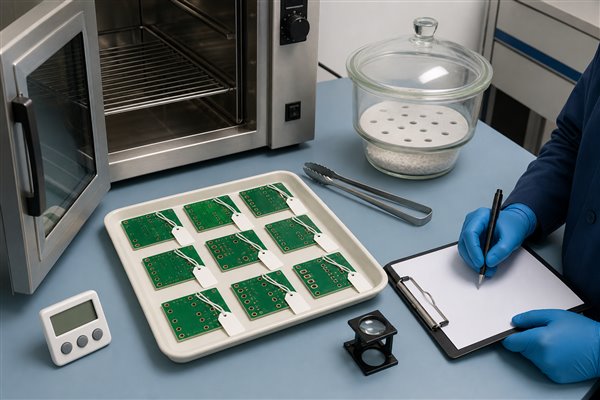
For boards held in storage, the production date alone is not a complete description of their condition. Whether the original packaging stayed intact and whether surfaces were exposed to contamination are also relevant. Baking should not be treated as a universal way to restore solderability: a moisture-removal step cannot simply reverse oxidation or damaged surface chemistry.
Is J-STD-003 Class 3 the Same as Coating Durability?
No. J-STD-003 Class 3 concerns the product classification; coating durability is a separate rating. A higher product class does not automatically specify an aging treatment.
In J-STD-003D, coating-durability notation differs between Pb-containing and Pb-free finishes. Category 2 or Category 3 terminology must not be exchanged blindly with the lettered categories for another finish system. Your specified revision and finish determine the applicable requirements.
What Is the J-STD-003 Latest Revision?
The J STD 003 latest revision listed when this article was checked in September 2026 is J-STD-003D. Older J-STD-003B and J-STD-003C references still appear in drawings and search results; they should not be treated as interchangeable editions.
If an existing design calls for an earlier revision, changing its acceptance basis is an engineering decision, not just a document-name update. We work from the agreed fabrication requirements rather than silently substituting a newer edition.
How Is J-STD-003 Different from J-STD-002 and J-STD-001?
The main difference is what is being evaluated: the bare board, the component connection surface, or the assembled soldered connection. The related standards are complementary, not substitutes.
Standard
Primary subject
J-STD-003
Printed-board solderability
J-STD-002
Solderability of component leads, terminations and related connection surfaces
J-STD-001
Requirements for soldered electrical and electronic assemblies
J-STD-004
Soldering flux requirements
J-STD-005 / J-STD-006
Solder paste / electronic-grade solder alloys and related forms
For example, a connector joint joins a board barrel to a component pin. Evaluating the barrel does not establish the pin’s solderability, while evaluating both surfaces still leaves the production soldering process to be controlled. This is why one bare-board test result cannot stand in for complete assembly acceptance.
How Do We Connect Bare-Board Quality with PCB Assembly?
We provide PCB fabrication and PCB assembly services, including SMT, through-hole and mixed assembly. This lets us consider the solderable board surface together with the components and the planned assembly sequence.
Our FR4 manufacturing capability extends to 32 layers, with the final construction subject to engineering review. For a multilayer controller with dense surface-mount parts and through-hole connectors, the board stack-up, pad finish and thermal demands all affect how fabrication and assembly fit together. We review these requirements as a connected PCB project, not as an isolated finish choice.
Discuss your J-STD-003 requirement with our engineering team at sales@bestpcbs.com. We can review the fabrication drawing, surface finish and assembly plan, and confirm the applicable project requirements before production. Any dedicated test method, sampling arrangement or report requirement must be agreed for that project.
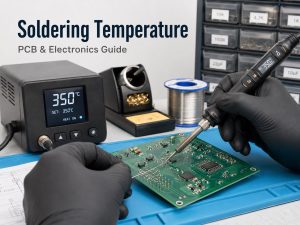
Choosing the right soldering temperature is not as simple as setting an iron to one number and using it for every joint. For most electronics work, a soldering iron tip is commonly set somewhere around 315–350°C (599–662°F) for leaded solder and 340–370°C (644–698°F) for common lead-free solder. These are practical starting ranges rather than universal limits.
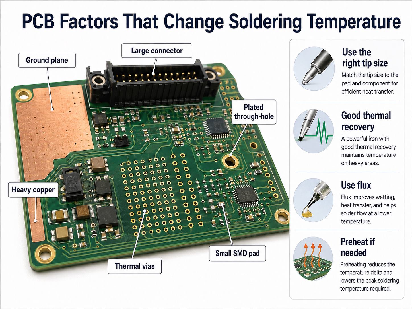
The correct setting also depends on solder alloy, PCB copper area, tip geometry, component size, flux activity, and how quickly the soldering station can replace lost heat. A small SMD pad may solder cleanly near the lower end of the range, while a connector tied to a large ground plane may need a larger tip, preheating, or a modest temperature increase.
What Is the Best Soldering Temperature for Electronics?
For general electronics soldering, about 320–350°C is a useful starting range for leaded solder, while 340–370°C is more typical for lead-free solder.
The temperature should be high enough to heat the pad, component lead, and solder quickly, but not so high that flux burns away before the joint forms.
A practical starting point is:
Fine electronic wiring or small pads: 300–330°C
General PCB work with leaded solder: 320–350°C
General PCB work with lead-free solder: 340–370°C
Large connectors or high-copper areas: often near the upper end of the range, preferably with a larger tip or PCB preheating
The best soldering temperature is therefore the lowest setting that can bring the entire joint to soldering temperature within a short, controlled contact time.
If the iron must remain on the joint for a long time, simply using a lower temperature is not necessarily gentler. Extended heating can transfer more total energy into the PCB and component than a slightly hotter tip used briefly.
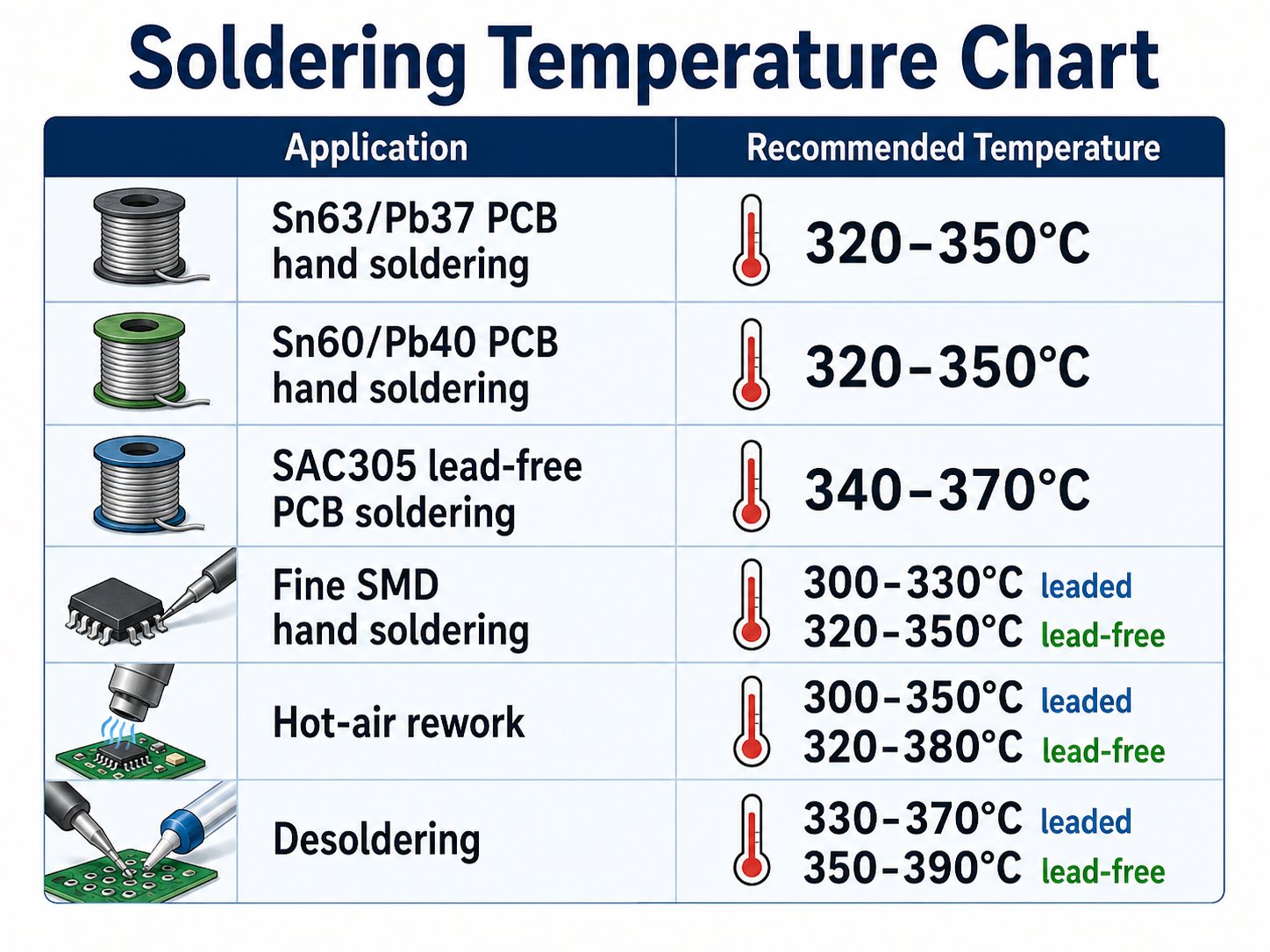
Soldering Temperature Chart for PCB and Electronics
The following soldering temperature chart provides practical starting values for common electronics work.
Application
Solder / Process
Melting or Liquidus Temperature
Practical Starting Setting
General PCB hand soldering
Sn63/Pb37
183°C
320–350°C
General PCB hand soldering
Sn60/Pb40
About 183–190°C
320–350°C
Lead-free PCB soldering
SAC305
About 217–220°C
340–370°C
Fine SMD hand soldering
Leaded
About 183°C
300–330°C
Fine SMD hand soldering
Lead-free
About 217–220°C
320–350°C
Large PCB connector
Leaded
About 183–190°C
340–370°C*
Large PCB connector
Lead-free
About 217–220°C
350–380°C*
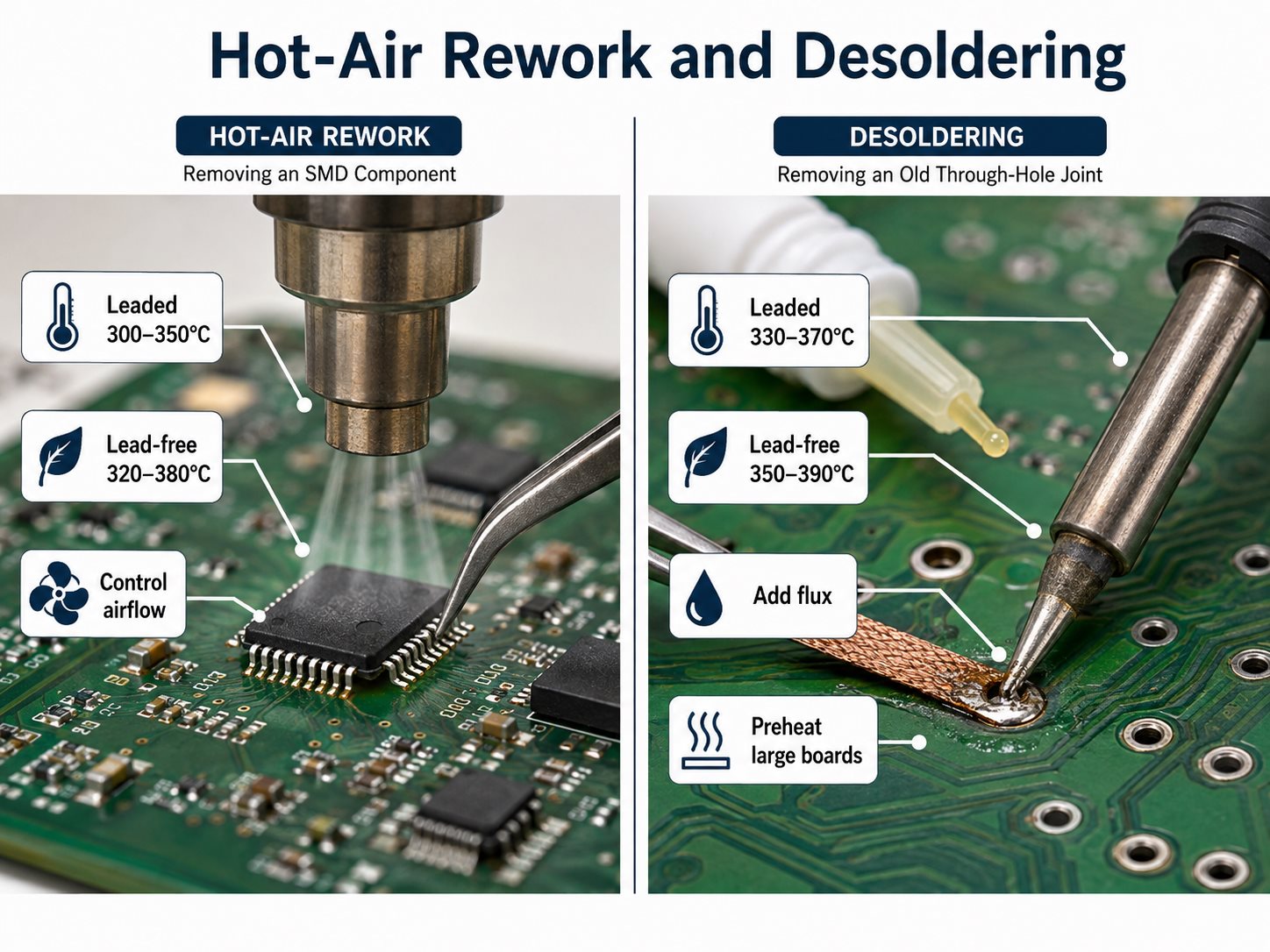
Leaded hot-air rework
Process dependent
—
About 300–350°C display setting*
Lead-free hot-air rework
Process dependent
—
About 320–380°C display setting*
Leaded desoldering
SnPb
About 183–190°C
330–370°C*
Lead-free desoldering
SAC-type alloy
About 217–220°C
350–390°C*
*These values depend strongly on thermal mass, equipment calibration, nozzle or tip size, airflow, and preheating.
The table should be treated as a setup reference rather than a process specification. The actual solder joint temperature is different from the temperature shown on the soldering station.
Why Is Soldering Iron Temperature Higher Than the Solder Melting Point?
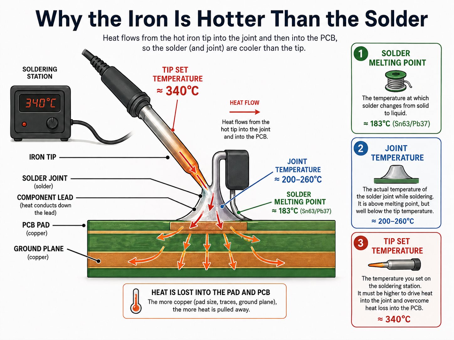
A soldering iron is normally set far above the solder’s melting point because heat must travel from the heater through the tip and into the complete joint.
For example, Sn63/Pb37 solder melts at 183°C, but setting an iron to 183°C would usually provide very little thermal margin. As soon as the tip touches a copper pad, heat begins flowing into:
the copper track,
plated through-hole barrel,
component lead,
nearby copper planes,
and the PCB laminate.
The tip surface can cool substantially during this transfer.
This is why melting temperature and soldering iron temperature are not interchangeable measurements.
Three temperatures are especially easy to confuse:
Solder melting temperature: where the alloy changes state.
Joint temperature: the temperature actually reached by the pad, lead, and solder.
Tip set temperature: the value selected on the soldering station.
A good soldering station compensates quickly when the tip loses heat. A weak station may show 350°C on the display yet struggle on a large ground connection because its heater cannot restore tip temperature fast enough.
What Soldering Temperature Should You Use for 60/40 and 63/37 Solder?
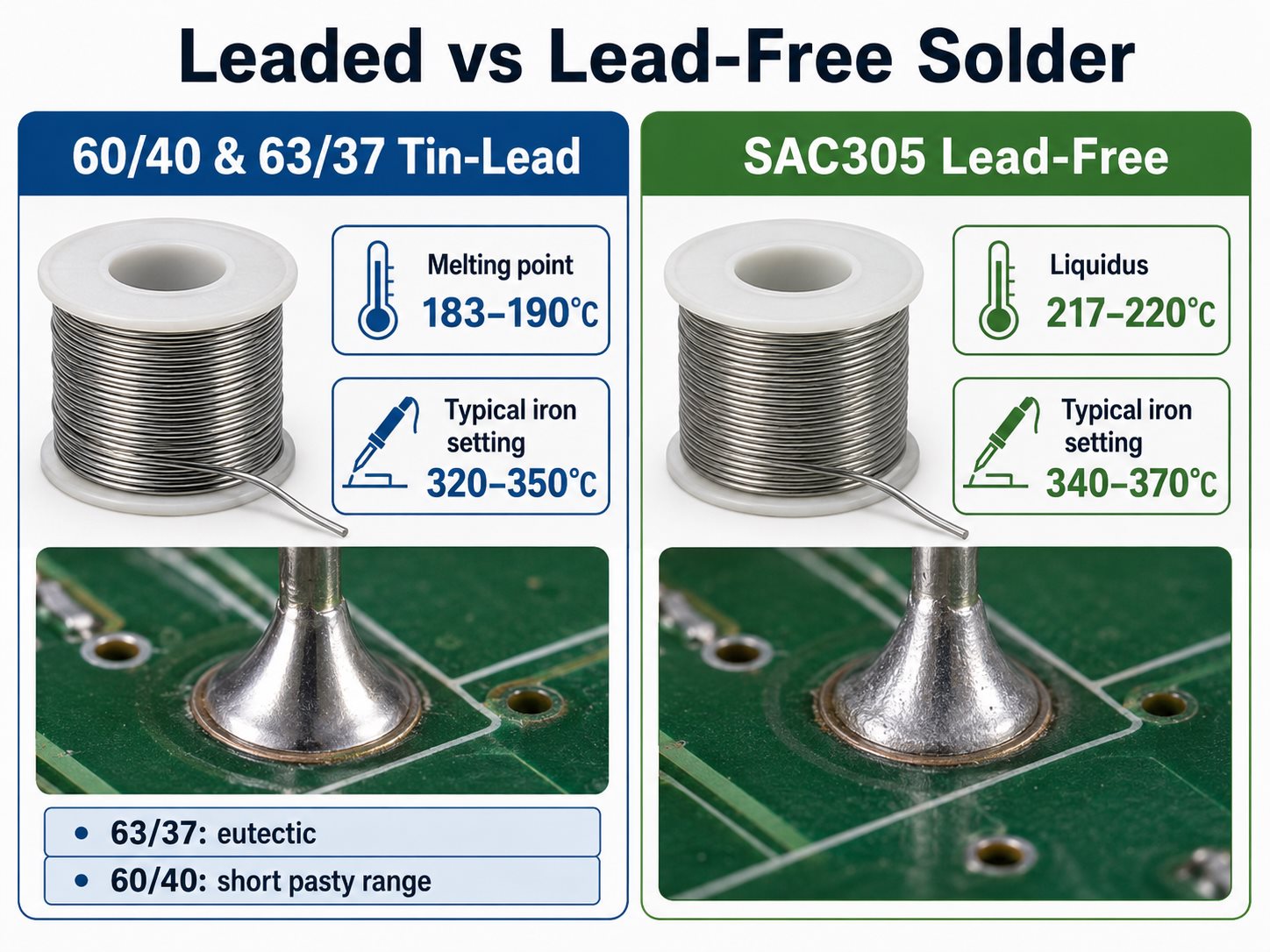
For 60/40 and 63/37 tin-lead solder, approximately 320–350°C is a practical hand-soldering starting range for normal PCB work.
The two alloys behave slightly differently.
Sn63/Pb37 is eutectic. It changes from solid to liquid at approximately 183°C without a significant pasty range. This makes the joint relatively easy to form and inspect during hand soldering.
Sn60/Pb40 begins melting at approximately 183°C and becomes fully liquid at around 190°C. It passes through a short plastic or pasty range during cooling.
For both alloys:
Small pads can normally use the lower end of the temperature range.
Larger terminals may require 340–350°C or slightly more.
Large ground planes should first be addressed with a larger tip or preheater rather than excessive temperature.
Good flux activity can reduce the time required to achieve complete wetting.
The difference between 60/40 and 63/37 is important, but PCB thermal mass usually has a greater effect on the required iron setting.
What Is the Best Soldering Temperature for Lead-Free Solder?
For common lead-free electronics solder such as SAC305, 340–370°C is a practical starting range for hand soldering.
Lead-free solder typically has a higher melting temperature than traditional SnPb solder. SAC305, for example, has a liquidus temperature around 217–220°C.
However, its higher working temperature does not mean every lead-free joint should automatically be soldered at 380°C or 400°C.
A better approach is to start around 340–350°C and increase only when the joint cannot reach temperature quickly enough.
Lead-free soldering also benefits from:
an appropriately sized chisel or bevel tip,
a station with good thermal recovery,
active flux,
clean and well-tinned tip surfaces,
and PCB preheating for large thermal masses.
Lead-free processes can oxidize tips faster, so continuously increasing temperature to compensate for a poorly wetted or oxidized tip usually makes the situation worse.
What Soldering Iron Temperature Should You Use for PCB Work?
For most PCB hand soldering, about 320–350°C for SnPb solder and 340–370°C for lead-free solder provides a useful starting window.
The PCB construction determines how much heat the joint absorbs.
A small pad on a standard two-layer FR-4 board may reach soldering temperature almost immediately. The same component lead connected to a multilayer ground plane can pull heat away from the tip much faster.
Pay particular attention to:
Ground and power planes: internal copper spreads heat away from the joint.
Large plated through-holes: the barrel conducts heat through the board thickness.
Large connectors: metal housings and thick pins act as heat sinks.
Thermal vias: arrays of vias can transfer heat into internal or opposite-side copper.
Metal-core boards: heat can leave the soldering area rapidly.
When a PCB joint is difficult to solder, using a larger tip with better contact area is often more effective than immediately turning the station hotter.
What Is the Proper SMD Soldering Temperature?
For small SMD hand soldering, about 300–330°C for leaded solder and 320–350°C for lead-free solder is often sufficient when the tip size and flux are appropriate.
Small components have little thermal mass, so they normally do not require the same thermal input as a large connector.
For packages such as 0402, 0603, SOIC, or fine-pitch IC leads, temperature control matters because the pad area is small and repeated heating can weaken the pad-to-laminate bond.
For cleaner SMD work:
Use a tip that matches the pad geometry.
Apply flux before touching the joint.
Keep contact time short.
Avoid pressing the tip into the pad.
Allow the joint to cool before repeated rework.
Use hot air or controlled reflow methods when a package cannot be heated evenly with an iron.
A high temperature is not automatically faster if the tip is too small to transfer heat efficiently.
What Hot Air Soldering Temperature Should You Use for PCB Rework?
For PCB hot-air rework, roughly 300–350°C for leaded assemblies and 320–380°C for lead-free assemblies can be used as initial station settings, but airflow and PCB preheating are equally important.
A hot-air station does not behave like a soldering iron. The displayed temperature is the heater or calibrated air temperature, not necessarily the temperature at the solder joint.
Actual heating depends on:
nozzle diameter,
airflow,
nozzle-to-board distance,
component size,
board thickness,
copper distribution,
surrounding components,
and whether the PCB is preheated.
A thick multilayer PCB may require a higher displayed air temperature than a thin board, even when the target solder joint temperature is similar.
For large BGAs, QFNs, shielded modules, or high-copper boards, preheating the PCB reduces the temperature difference between the rework area and the rest of the board. This generally allows gentler top-side heating and reduces local thermal stress.
What Desoldering Temperature Should You Use?
For desoldering, about 330–370°C for leaded joints and 350–390°C for lead-free joints is a reasonable starting range, depending on board construction and the removal method.
Old solder can be more difficult to remove because of oxidation, contamination, or poor remaining flux activity.
Before raising the temperature, try:
applying fresh flux,
adding a small amount of fresh solder,
using a wider desoldering tip,
improving contact with the joint,
preheating large multilayer boards,
or using a powered desoldering tool for plated through-holes.
Adding fresh solder may seem counterintuitive, but it introduces active flux and improves heat transfer into an old joint.
Extra care is required on plated through-holes. Excessive temperature combined with prolonged heating can damage pad adhesion or the connection between the hole barrel and internal copper layers.
What Factors Change the Proper Soldering Temperature?
The proper soldering temperature is primarily determined by how efficiently heat moves from the tool into the solder joint.
The most important variables are:
Solder alloy: lead-free alloys generally require higher process temperatures than SnPb alloys.
Copper area: large pads, planes, and heavy copper remove heat rapidly.
Tip geometry: a larger contact surface transfers energy more efficiently.
Station power and recovery: higher heater capacity helps maintain tip temperature under load.
Flux condition: active flux improves wetting and reduces the time needed to form the joint.
Component thermal mass: connectors, switches, shields, and large terminals absorb more heat.
PCB thickness: thick multilayer boards usually require more thermal energy.
Preheating: raising the overall PCB temperature can reduce the heat demanded from the soldering tool.
Contact time: temperature and dwell time must be considered together.
A station temperature therefore cannot be selected from solder alloy alone. Two assemblies using SAC305 may require noticeably different settings because one has small SMD pads while the other has a large connector tied to a power plane.
How Can You Tell If the Soldering Temperature Is Too High or Too Low?
The condition of the joint often shows whether the soldering temperature or heat-transfer setup needs adjustment.
Temperature Too Low / Heat Transfer Too Weak
Temperature Too High / Heating Too Aggressive
Solder does not wet the pad easily
Flux burns or smokes excessively
Joint looks dull, uneven, or incomplete
Tip oxidizes quickly
Solder forms a ball instead of spreading
PCB surface discolors
Long contact time is required
Pads may loosen or lift
Large joints refuse to flow
Plastic connectors may deform
Excessive pressure is needed with the iron
Components experience unnecessary thermal stress
A cold-looking joint does not always mean the temperature setting is too low. An oxidized tip, insufficient flux, a very small tip, or a large ground plane can produce similar symptoms.
Likewise, a joint that takes too long at 350°C may be improved by switching from a fine conical tip to a larger chisel tip instead of increasing the iron to 400°C.
FAQs About Soldering Temperature
Is 350°C too hot for PCB soldering?
No. Around 350°C is a common working temperature for many PCB soldering operations, particularly lead-free work or joints with moderate thermal mass. For small heat-sensitive pads, a lower setting may be more appropriate.
What is the normal soldering temperature for electronics?
A typical starting range is approximately 320–350°C for leaded solder and 340–370°C for lead-free solder. The final setting should be adjusted according to joint size, tip geometry, copper area, and contact time.
What temperature should I use for 60/40 solder?
For normal PCB hand soldering with Sn60/Pb40, start around 320–350°C. The alloy melts over approximately 183–190°C, but the iron must be hotter to transfer sufficient heat into the complete joint.
What temperature should I use for lead-free solder?
For common lead-free solder such as SAC305, around 340–370°C is a practical hand-soldering range. Large copper areas may require more thermal capacity, but a larger tip or preheater should usually be considered before using substantially higher temperatures.
Why won’t solder melt even when my iron is hot?
The tip may be oxidized, too small, poorly wetted, or unable to transfer enough heat into the joint. Large ground planes and connectors can also draw heat away faster than the soldering station can replace it.
Can too much heat lift PCB pads?
Yes. Excessive temperature, prolonged contact, repeated rework, and mechanical force can weaken pad adhesion and increase the risk of pad lifting. Controlled temperature, suitable tip geometry, flux, and short contact time reduce this risk.
How Can EBest Circuit Support Your PCB Assembly Project?
If you are preparing a PCB or PCBA project and need support with soldering process requirements, assembly manufacturability, or production planning, send your Gerber files, BOM, and assembly requirements tosales@bestpcbs.com. Our engineering team can review the project before production and help identify process conditions that may affect solder-joint quality, component reliability, or assembly yield.
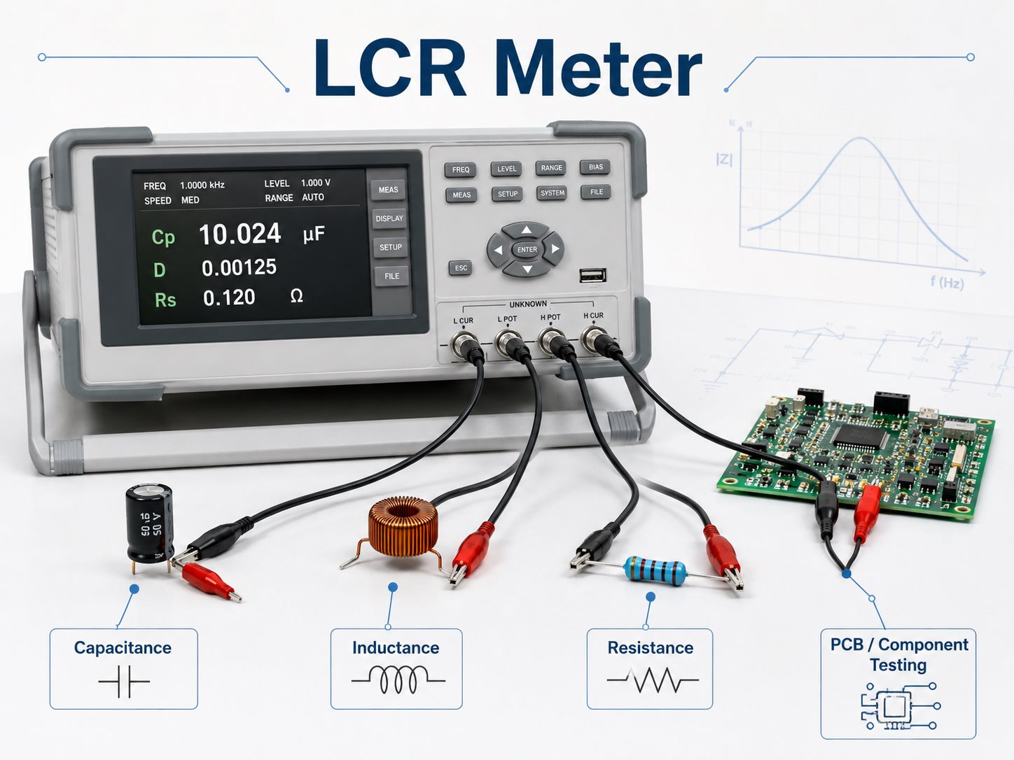
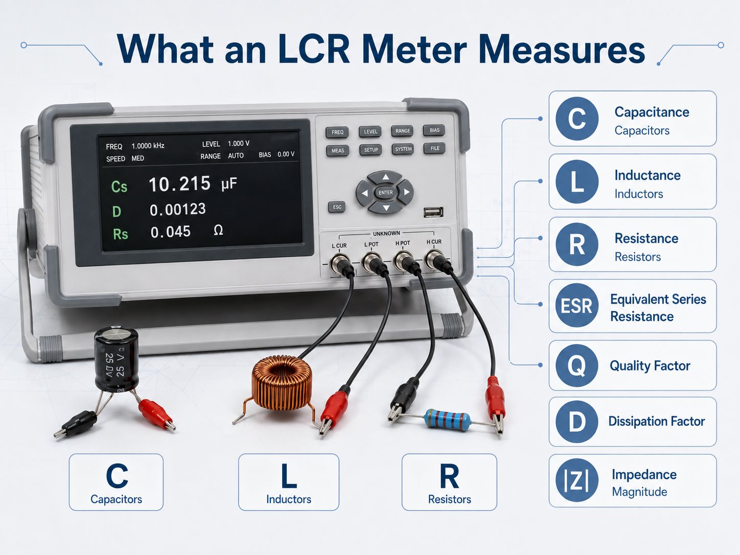
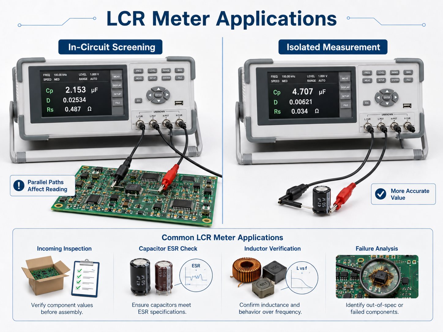
An LCR meter measures the electrical behavior of resistors, capacitors, inductors, coils, and other passive components under an AC test signal. Unlike a basic multimeter, it can show not only resistance or capacitance, but also impedance, ESR, Q factor, dissipation, and phase-related parameters.
That matters because real components are not ideal. A capacitor has resistance and parasitic inductance. An inductor has winding resistance and stray capacitance. Their measured values can change with frequency, fixture setup, temperature, and even the surrounding PCB circuit.
This guide explains how an LCR meter works, how to choose the right measurement settings, and how to use it for component and PCB testing.
What Is an LCR Meter?
An LCR meter is an electronic instrument used to measure inductance (L), capacitance (C), and resistance (R).
The name comes from its three main parameters:
L — Inductance, measured in henries (H)
C — Capacitance, measured in farads (F)
R — Resistance, measured in ohms (Ω)
A digital LCR meter normally measures these parameters by applying a controlled AC signal rather than relying only on DC measurement.
This makes it useful for checking components whose electrical behavior changes with frequency, including:
ceramic and electrolytic capacitors;
inductors and chokes;
transformer windings;
precision resistors;
PCB coils and planar inductors.
For basic component identification, a simple handheld unit may be enough. More demanding laboratory or production measurements usually require tighter accuracy, controlled fixtures, and a wider test-frequency range.
What Does an LCR Meter Measure Besides L, C, and R?
L, C, and R are only the starting point. Many LCR meters also calculate secondary parameters that show how much loss or parasitic behavior a component has.
Parameter
Meaning
Typical Use
L
Inductance
Inductors, coils
C
Capacitance
Capacitors
R
Resistance
Resistors, winding resistance
Z
Impedance
Overall AC behavior
ESR
Equivalent series resistance
Capacitor loss
Q
Quality factor
Inductor performance
D
Dissipation factor
Capacitor loss
θ
Phase angle
Reactive behavior
For example, two capacitors may both measure close to 100 µF, yet one may have much higher ESR. In a power circuit, that difference can affect ripple, heating, and stability even though the capacitance reading looks acceptable.
Q factor is commonly used for inductors. It compares reactive behavior with resistive loss at a specified frequency. Dissipation factor performs a similar role for capacitors.
Because these values are frequency-dependent, an ESR or Q reading is much more useful when the test frequency is also recorded.
How Does an LCR Meter Work?
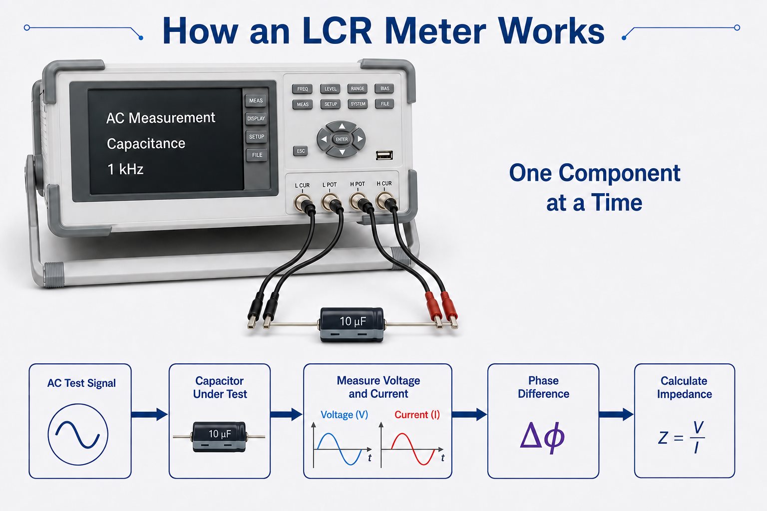
An LCR meter applies a known AC signal to the device under test and measures how the component responds.
The measurement sequence is roughly:
Generate an AC test signal.
Apply it to the component.
Measure voltage and current.
Determine the phase difference between them.
Calculate complex impedance.
Convert the result into L, C, R, ESR, Q, D, or another selected parameter.
The AC signal is important because capacitors and inductors respond differently as frequency changes.
For a capacitor: Xc = 1 / (2πfC)
For an inductor: XL = 2πfL
As frequency rises, capacitive reactance falls while inductive reactance rises.
A more precise benchtop LCR meter may also use automatic balancing bridge techniques and four-terminal-pair connections. These methods reduce errors caused by test leads, contact resistance, and fixture parasitics.
Why Does Test Frequency Matter in LCR Measurements?
The same component can produce different LCR readings at different frequencies.
This is normal. Real components contain parasitic elements that become more or less significant as frequency changes.
Typical examples include:
Large electrolytic capacitors are often characterized at relatively low frequencies.
Small ceramic capacitors may be measured at 1 kHz or higher, depending on the specification.
Power inductors are commonly tested differently from small RF inductors.
An RF inductor can change behavior significantly as the test frequency approaches self-resonance.
A capacitor, for example, does not consist of capacitance alone. Its equivalent circuit also includes ESR and parasitic inductance. At low and moderate frequencies, capacitance may dominate. At sufficiently high frequencies, parasitic inductance becomes much more important.
For component acceptance testing, the best practice is simple:
Use the measurement frequency stated in the component datasheet or applicable test specification.
If the test is for troubleshooting rather than formal verification, choose a frequency relevant to the application and keep it consistent when comparing suspect and known-good components.
What Is the Difference Between Series and Parallel Measurement Modes?
Series and parallel modes are equivalent circuit models used to represent the losses in a real component.
Common settings include:
Cs — series capacitance
Cp — parallel capacitance
Ls — series inductance
Lp — parallel inductance
Rs — series resistance
Rp — parallel resistance
They do not mean that the physical component changes internally. The meter is simply expressing the same impedance using a different mathematical model.
As a practical rule:
Lower-impedance devices are often represented with a series model.
Higher-impedance devices are often represented with a parallel model.
The correct setting depends on the device, frequency, and test specification.
This becomes important when checking lossy capacitors or inductors. Cs and Cp, or Ls and Lp, may not give identical numerical results. If a datasheet specifies one equivalent model, use that same model during verification.
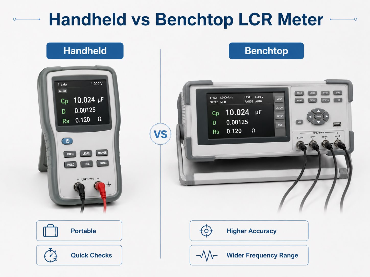
Handheld vs Benchtop LCR Meter: What Is the Difference?
The main difference is not simply portability. It is the amount of control the instrument gives over the measurement.
Feature
Handheld LCR Meter
Benchtop LCR Meter
Portability
High
Low
Frequency range
Usually narrower
Usually wider
Accuracy
General-purpose
Higher precision
Fixtures
Basic
More options
Bias capability
Limited
More common
Automation
Limited
Often supported
Typical use
Repair, field work
R&D, QC, production
A handheld LCR meter is useful for:
maintenance;
component sorting;
quick incoming checks;
general troubleshooting.
A benchtop unit is more appropriate when a test requires:
tighter tolerances;
repeatable fixtures;
multiple test frequencies;
DC bias;
automated data collection;
production pass/fail limits.
The right choice depends on what needs to be measured, not on whether one instrument has more features.
LCR Meter vs Multimeter: What Is the Difference?
A multimeter is designed for general electrical troubleshooting. An LCR meter is designed to characterize passive components under controlled AC conditions.
A typical multimeter measures:
AC/DC voltage;
current;
resistance;
continuity;
diode behavior.
Some models also provide basic capacitance or frequency functions.
An LCR meter can usually measure:
inductance;
capacitance;
resistance;
impedance;
ESR;
Q factor;
dissipation factor;
phase angle.
It also allows the user to select test frequency and, on many models, the equivalent circuit.
For checking whether a 1 kΩ resistor is open, a multimeter is sufficient.
For determining whether an inductor still meets its inductance and Q requirements, or whether a capacitor has excessive ESR, an LCR meter gives much more useful information.
How to Use an LCR Meter?
A reliable LCR measurement depends on both the instrument settings and the test setup.
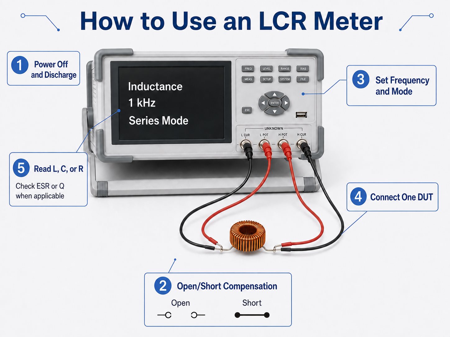
A practical workflow is:
Power off the circuit. Passive LCR measurements should not normally be made on an energized circuit.
Discharge capacitors. Stored charge can distort the reading or damage the meter input.
Choose the correct fixture. SMD tweezers work well for small chip components. Kelvin clips or dedicated fixtures improve repeatability for low-impedance measurements.
Perform open and short compensation. This reduces errors from leads, fixtures, stray capacitance, and residual impedance.
Select the main parameter. Choose L, C, R, Z, or automatic detection if supported.
Set the test frequency. Match the datasheet condition when verifying a rated value.
Choose series or parallel mode. Use the mode specified for the component whenever possible.
Connect the component securely. Poor contact can cause unstable or inflated readings.
Read the secondary parameter as well. Capacitance plus ESR, or inductance plus Q, is often more informative than the primary value alone.
Compare under the same conditions. Frequency, fixture, temperature, and circuit model should remain consistent between measurements.
For repeated inspection, document the meter settings in the test instruction. Otherwise two operators can test the same component and obtain different results simply because they used different frequencies or modes.
Can You Measure Components Directly on a PCB with an LCR Meter?
Yes, but an in-circuit reading may include the electrical effect of other components connected around the part.
This is especially common with:
capacitors connected in parallel on a power rail;
resistors forming parallel current paths;
transformer or inductor windings connected to other circuitry;
semiconductor junctions;
passive filter networks.
Suppose several capacitors share the same supply rail. Measuring one capacitor without removing it may effectively measure part of the entire network rather than that single component.
In-circuit LCR measurements are still useful for quick screening. A technician may compare a suspect PCB with a known-good board and look for a major difference.
For an accurate standalone value, it may be necessary to:
lift one terminal;
remove the component;
isolate the surrounding circuit;
test the part in a dedicated fixture.
A strange in-circuit reading should therefore be treated as a diagnostic clue, not immediate proof that the component has failed.
What Causes Incorrect LCR Meter Readings?
Many incorrect readings come from the setup rather than the component itself.
Common causes include:
Wrong test frequency — the component is being measured under conditions different from its datasheet rating.
Wrong equivalent model — Cs/Cp or Ls/Lp selection changes the reported value.
No open/short compensation — lead and fixture parasitics become part of the result.
Poor contact — oxidized leads or unstable clips add resistance.
Long test leads — extra inductance and capacitance become significant.
In-circuit paths — nearby components alter the measured impedance.
Temperature change — many passive components have measurable temperature coefficients.
DC bias effects — some ceramic capacitors lose effective capacitance under applied bias.
Contamination — moisture, flux residue, or dirt can affect high-impedance and low-capacitance measurements.
Operating near the meter limits — accuracy usually falls when the component value is close to the instrument’s practical measurement range.
Fixture parasitics deserve particular attention when measuring very small capacitance or inductance. A few picofarads of stray capacitance may be negligible when measuring microfarads, but very significant when the DUT itself is only a few picofarads.
Low-resistance and low-inductance measurements similarly benefit from Kelvin or four-wire techniques because ordinary test-lead resistance can become comparable to the device being measured.
How Are LCR Meters Used in PCB and PCBA Testing?
LCR meters are useful in PCB and PCBA work when a simple resistance or continuity check does not provide enough information.
Typical applications include:
Incoming component inspection — verifying resistor, capacitor, and inductor values before assembly.
Capacitor troubleshooting — checking capacitance, ESR, or dissipation in unstable power circuits.
Inductor and coil verification — measuring inductance, winding resistance, and Q.
Transformer checks — comparing winding parameters with approved samples.
Alternative-part verification — confirming that a substitute passive component matches the required electrical behavior.
First-article troubleshooting — checking suspect components against BOM or datasheet requirements.
Failure analysis — identifying parameter drift after thermal or electrical stress.
Printed coil testing — measuring PCB inductors, planar coils, and similar structures after fabrication.
The measurement procedure should define more than a nominal component value.
For production or quality inspection, useful test requirements normally include:
test frequency;
allowable tolerance;
fixture type;
series or parallel mode;
secondary parameter limits where relevant.
For PCB coils, transformers, RF structures, and precision analog circuits, these conditions are especially important because parasitic behavior is part of the real electrical performance.
FAQs About LCR Meters
What does LCR stand for on a meter? LCR stands for inductance, capacitance, and resistance. These are the three primary passive-component parameters measured by the instrument.
Can an LCR meter measure ESR? Yes, many digital LCR meters can measure or calculate equivalent series resistance. ESR is commonly used when evaluating capacitor loss.
Why does capacitance change when I change the test frequency? Real capacitors contain ESR, dielectric losses, and parasitic inductance. Their combined impedance changes with frequency, so the calculated capacitance may also change.
Is an LCR meter better than a multimeter for testing capacitors? For detailed capacitor characterization, usually yes. An LCR meter can measure capacitance together with ESR, dissipation, and frequency-dependent behavior that a basic multimeter cannot show.
Can I test a capacitor without removing it from the PCB? You can perform an in-circuit screening test, but parallel components may influence the reading. Isolate or remove the capacitor when an accurate standalone value is required.
What frequency should I use on an LCR meter? Use the frequency specified in the component datasheet when checking compliance with a rated value. For troubleshooting, use a frequency appropriate to the application and keep it consistent between comparisons.
How Can EBest Circuit Support Your PCB and PCBA Project?
If you need PCB or PCBA manufacturing support involving passive-component verification, printed coils, electrical testing, or assembly troubleshooting, send your Gerber files, BOM, and test requirements to sales@bestpcbs.com.
Electronic equipment can remain useful long after one of its circuit boards begins to age or fail. A damaged relay, degraded capacitor, corroded connector, cracked solder joint, or localized PCB defect does not always justify replacing the complete assembly.
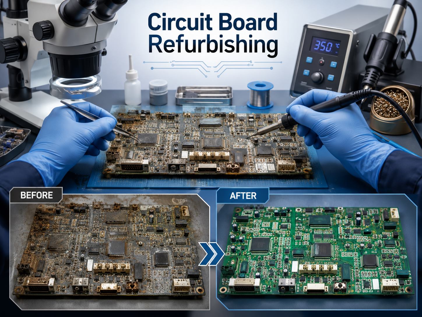
Circuit board refurbishing restores an aged, damaged, or failed electronic board to a usable and verified condition. Depending on the board, the work may involve troubleshooting, cleaning, component replacement, solder rework, conductor repair, and functional testing.
It is particularly relevant to industrial electronics, legacy equipment, discontinued assemblies, and high-value boards where direct replacement may be difficult or uneconomical.
What Is Circuit Board Refurbishing?
Circuit board refurbishing is a broader restoration process than simply replacing one failed part.
Although the term “circuit board” is sometimes used for a bare PCB, refurbishment usually applies to a populated assembly containing components, connectors, solder joints, and interconnections.
Typical work can include:
replacing failed or degraded components;
repairing cracked or defective solder joints;
restoring damaged pads, traces, or vias;
cleaning corrosion and contamination;
repairing connectors and contacts;
removing and replacing damaged conformal coating;
checking areas affected by overheating;
testing the board after rework.
The objective is to restore the board to a condition where its required functions can be verified, not to make an old assembly physically identical to a newly manufactured one.
What Is the Difference Between Circuit Board Refurbishing and PCB Repair?
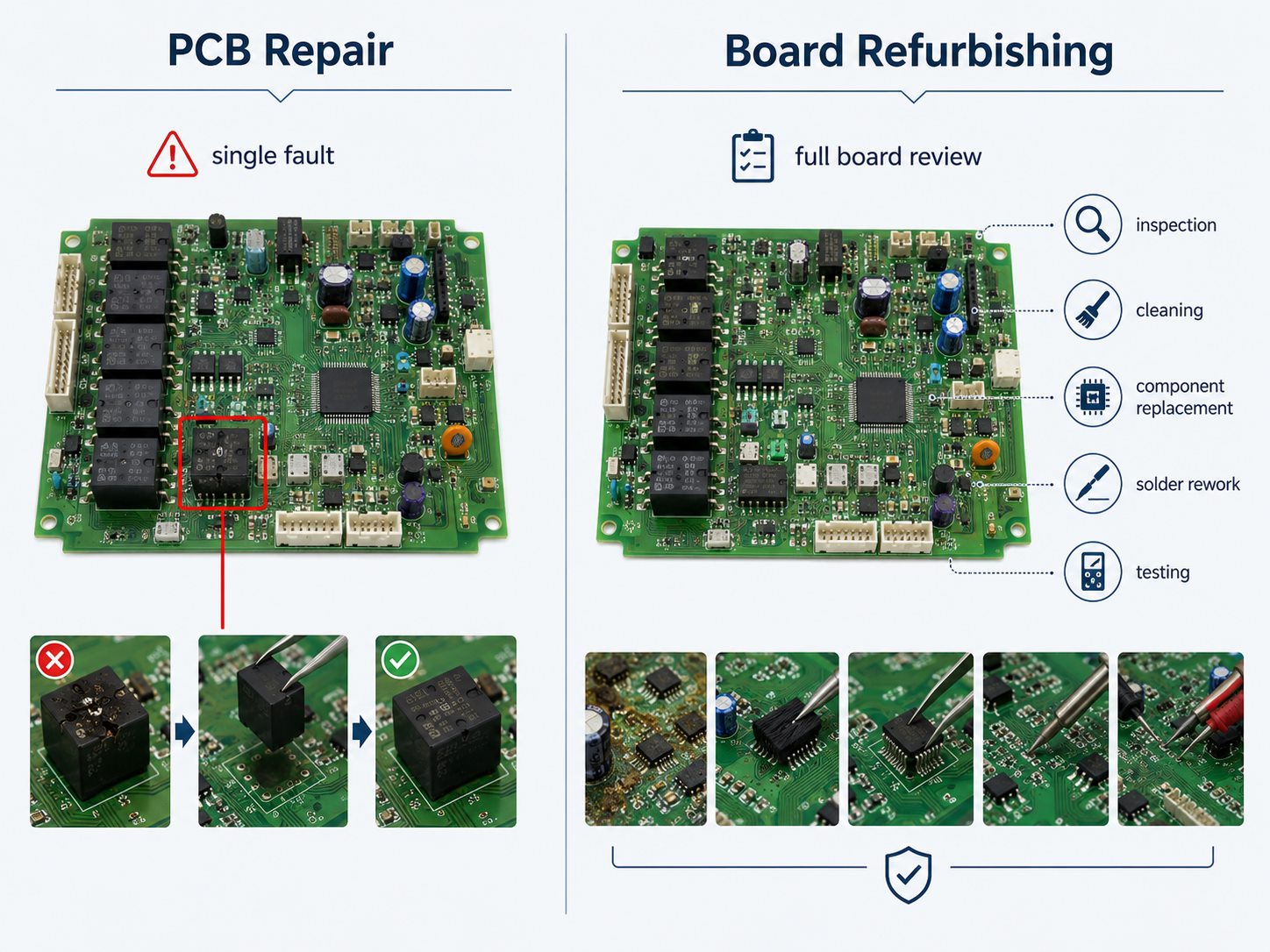
PCB repair normally targets a known fault, while circuit board refurbishing evaluates the board more broadly before returning it to service.
PCB Repair
Circuit Board Refurbishing
Usually starts with a specific fault
May start with failure, age, or deterioration
Focuses on the failed area
Looks at the wider board condition
Often replaces one defective part
May replace failed and selected aging parts
Main goal is fault correction
Main goal is restoring serviceability
Testing may focus on the repaired circuit
Testing may cover a wider range of board functions
For example, replacing a failed relay and checking its output is a repair. If the same board is also inspected for heat damage, deteriorated capacitors, connector corrosion, weak solder joints, and other age-related problems before being functionally tested, the work is closer to refurbishment.
Which Circuit Boards Are Good Candidates for Refurbishing?
Boards are generally worth evaluating when they are expensive, difficult to replace, or installed in equipment that still has useful service life.
Common candidates include:
industrial control boards;
PLC and automation electronics;
motor-drive boards;
power-control assemblies;
machine-tool electronics;
legacy instrumentation;
discontinued OEM boards;
proprietary low-volume assemblies;
equipment with long spare-part lead times.
The best candidates usually have localized faults and a mechanically sound PCB substrate.
Schematics, a BOM, service documentation, firmware information, a known-good board, or an existing test procedure can also make diagnosis much more practical.
What Problems Can Circuit Board Refurbishing Correct?
Refurbishment is most suitable for defects that can be isolated and repaired without rebuilding large portions of the PCB.
Common examples include:
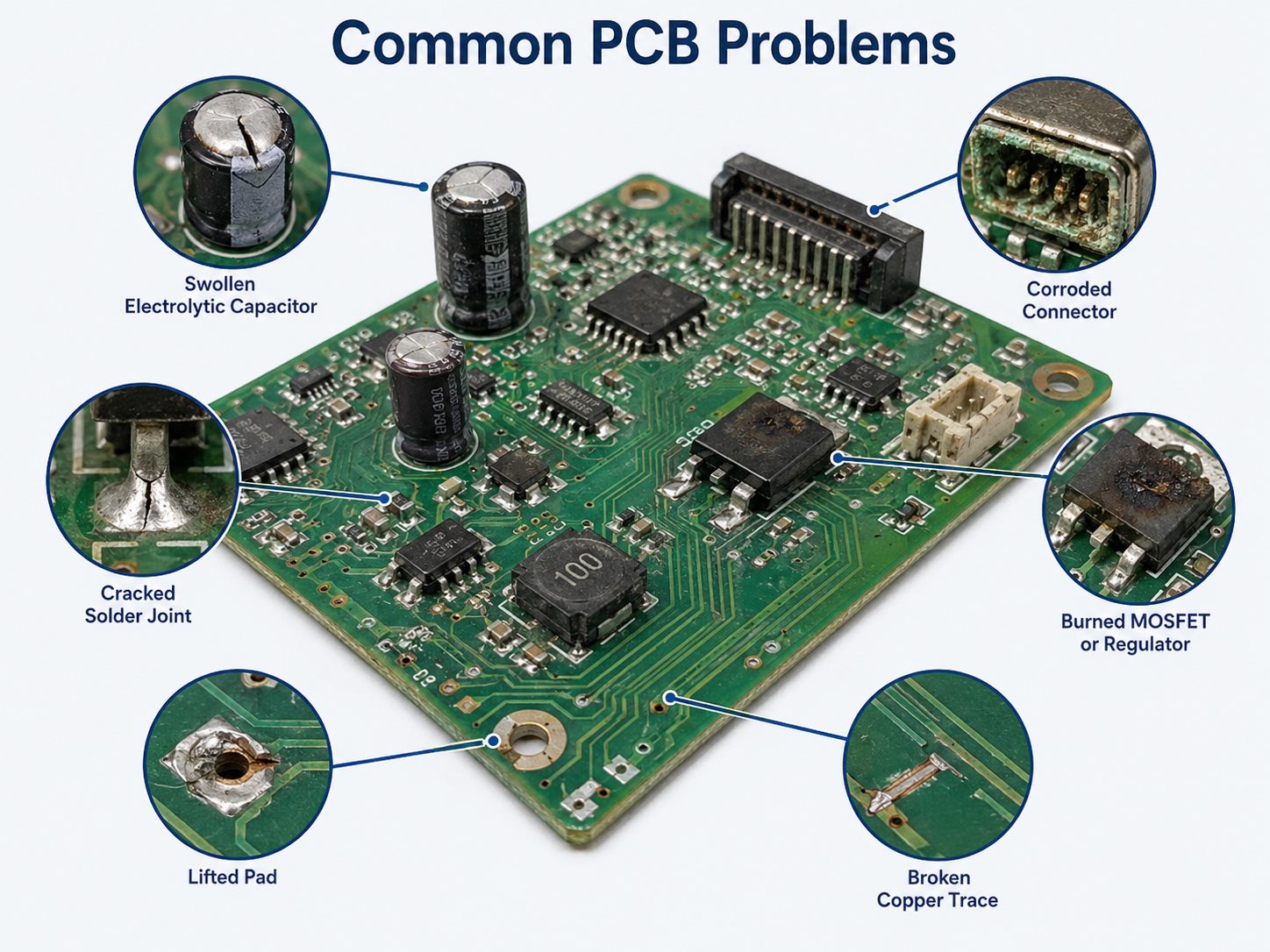
high-ESR or failed electrolytic capacitors;
worn relays;
oxidized or damaged connectors;
cracked solder joints;
failed MOSFETs, IGBTs, regulators, or diodes;
overheated resistors;
lifted pads;
broken copper traces;
damaged plated-through holes;
localized corrosion;
deteriorated conformal coating;
contamination from dust, moisture, or residues.
The visible failure is not always the root cause. A burned MOSFET may have failed because of a damaged gate-drive circuit, excessive load, or another power-stage problem.
Corrosion also needs careful assessment. Surface corrosion near a connector may be manageable, while corrosion beneath packages or inside vias can be much harder to restore reliably.
How Is a Circuit Board Refurbished?
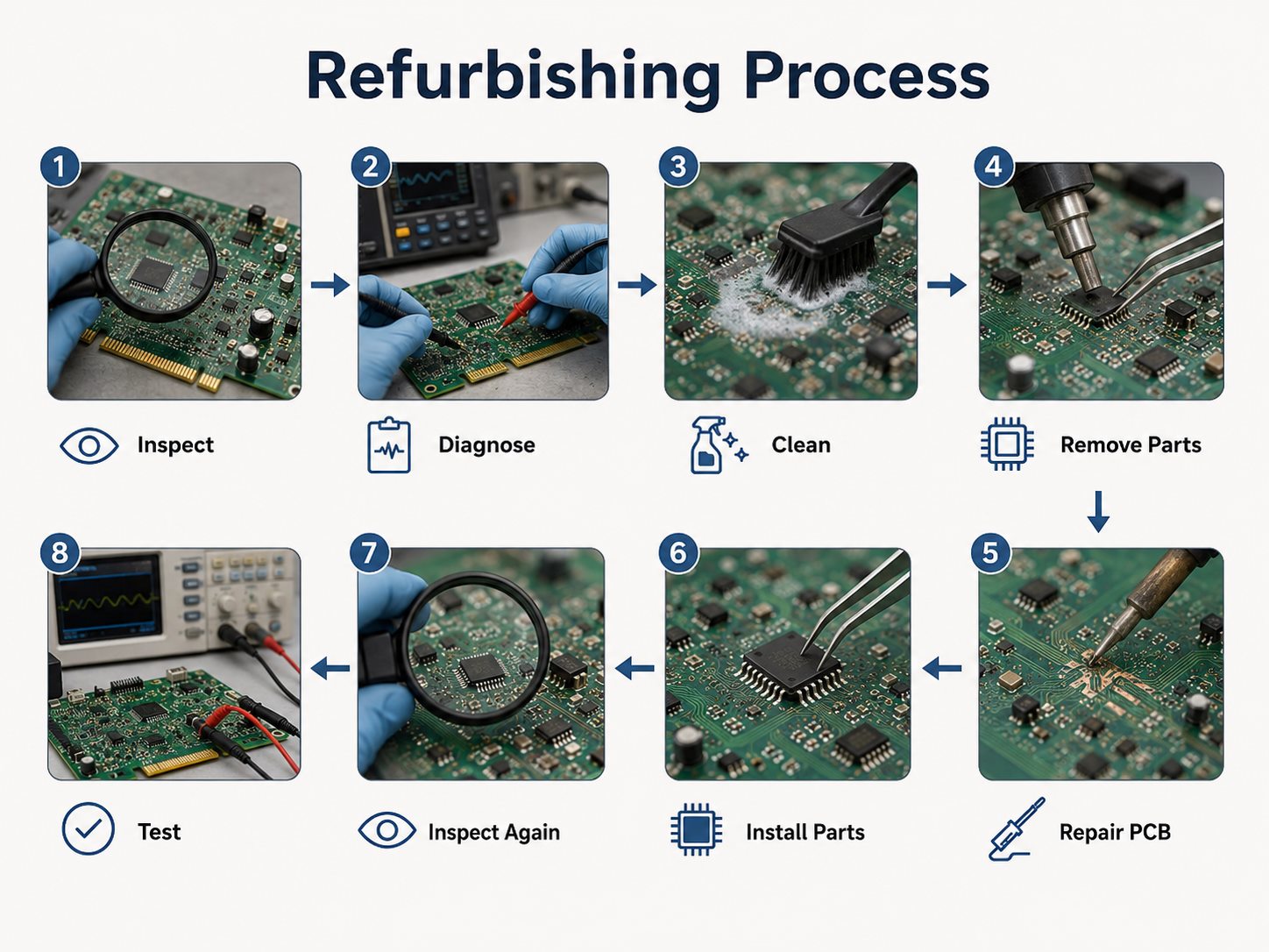
A typical refurbishment process moves from diagnosis to controlled rework and then verification.
1. Review the fault history
Record the board model, symptoms, operating conditions, previous repairs, and when the failure occurs. Intermittent, temperature-related, and load-related faults can point to different failure mechanisms.
2. Inspect the board
Visual and microscopic inspection may reveal:
burned components;
cracked joints;
corrosion;
damaged connectors;
swollen capacitors;
lifted pads;
coating damage;
previous poor-quality rework.
3. Diagnose the electrical fault
Testing may include continuity checks, resistance measurements, power-rail analysis, signal tracing, diode-mode measurements, and comparison with a known-good board.
4. Clean contaminated areas
Flux residue, dust, oils, and corrosion products may interfere with inspection or electrical performance. Proper cleaning of PCB assemblies after soldering helps technicians expose defects and remove residues. Cleaning materials must be compatible with the PCB, plastics, labels, coatings, and components.
5. Remove defective components
Removal technique depends on the package. A through-hole relay, small resistor, QFN, and BGA each require different tools and thermal control.
6. Repair PCB damage
Localized board restoration may include:
pad repair;
trace repair;
via repair;
conductor reinforcement;
solder-mask restoration;
limited laminate repair.
7. Install replacement parts
Replacement components must match the required electrical ratings, package, polarity, thermal capability, and circuit function.
8. Inspect and test
The reworked area is inspected before the board moves to electrical and functional verification.
Which Components Are Commonly Replaced During Refurbishing?
Components exposed to mechanical wear, heat, or gradual electrical degradation usually receive the most attention.
For basic work, a circuit board repair kit and suitable circuit board repair tools may cover through-hole components, but fine-pitch PCB refurbishment and PCB restoration require controlled heating, inspection, and test equipment.
Frequently evaluated parts include:
electrolytic capacitors;
relays;
connectors;
MOSFETs and IGBTs;
rectifiers;
voltage regulators;
optocouplers;
heat-stressed resistors;
damaged ICs.
Electrolytic capacitors are commonly checked because capacitance, ESR, leakage, and temperature exposure can change over time.
Relays may still actuate mechanically even when their contacts have become resistive or unreliable under load. Connectors can develop similar intermittent faults through oxidation, vibration, or repeated mating cycles.
Parts should not be replaced only because the board is old. Unnecessary rework adds thermal cycles and handling stress to the PCB.
How Are BGA and SMD Components Reworked During PCB Refurbishment?
Fine-pitch SMD and BGA refurbishment requires tighter process control than conventional through-hole repair.
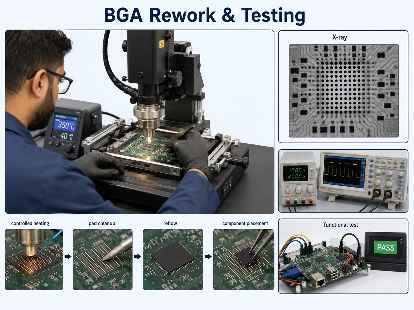
A BGA rework may involve:
confirming that the device or solder interface is defective;
protecting nearby components;
controlling top and bottom heating;
removing the package without lifting pads;
cleaning and inspecting the land pattern;
repairing damaged pads if necessary;
reballing or preparing the replacement component;
aligning and reflowing the device;
inspecting hidden joints by X-ray.
Poor thermal control can warp the PCB, damage laminate, lift pads, or overheat adjacent components.
QFN packages create a similar inspection challenge because part of the solder interface sits beneath the component and cannot be fully checked optically.
How Is a Refurbished Circuit Board Tested?
Testing should confirm that the original fault has been corrected without introducing another defect. A documented PCB inspection step also helps verify workmanship before functional testing.
Depending on the assembly, verification may include:
visual and microscopic inspection;
continuity and resistance checks;
short-circuit checks before power-up;
controlled power-up with current limiting;
voltage-rail verification;
signal and I/O testing;
communication testing;
relay or actuator operation;
functional testing;
load testing;
X-ray inspection for hidden joints;
thermal inspection.
Functional testing is particularly important. Confirming a 5 V rail, for example, does not prove that an industrial controller can read sensors, communicate with another device, drive its outputs, and remain stable under load.
When Is a Circuit Board Not Worth Refurbishing?
Refurbishment becomes difficult to justify when damage is widespread, structural, or impossible to verify after repair.
Warning signs include:
severe laminate carbonization;
extensive delamination;
major internal-layer damage;
widespread corrosion;
badly damaged BGA pad fields;
repeated previous repairs in the same area;
large areas affected by overheating;
unavailable proprietary ICs;
inaccessible firmware or programmed devices;
safety-critical boards without an approved repair route;
refurbishment cost close to the cost of replacement.
Carbonized PCB material deserves particular caution because it can become electrically conductive. Covering a burned area with coating or epoxy does not necessarily restore its original insulation properties.
Repeated heating can also weaken pads, plated-through holes, and laminate adhesion.
Circuit Board Refurbishing vs Replacement: Which Should You Choose?
Refurbishment usually makes the most sense when the board is valuable, difficult to replace, and affected by a localized fault that can be properly tested afterward.
Situation
More Practical Choice
OEM board is discontinued
Refurbish
Replacement lead time is long
Refurbish
High-value industrial board
Evaluate refurbishment
Failure is localized
Repair or refurbish
Extensive laminate damage
Replace
New board is inexpensive and available
Replace
Critical IC is unavailable
Replacement may be necessary
Functional testing is impossible
Further engineering evaluation
Several areas have repeatedly failed
Consider replacement
The comparison should include more than the price of the board. Downtime, machine qualification, software compatibility, installation work, spare-part availability, and equipment lifecycle can materially change the economics.
What Standards Apply to Circuit Board Rework and Refurbishment?
IPC-7711/7721 is one of the main references for electronic assembly rework, modification, and repair. It covers procedures associated with component removal and installation as well as land, conductor, laminate, and coating repair.
Other relevant standards can include:
J-STD-001 — requirements for soldered electrical and electronic assemblies;
IPC-A-610 — acceptance criteria for electronic assemblies.
The applicable requirement depends on the product, customer specification, assembly class, and industry.
Medical, aerospace, automotive, military, and other controlled applications may impose additional limits on permitted repairs and required documentation.
What Information Should You Provide for Circuit Board Refurbishing?
Clear fault information can reduce diagnostic time and help technicians reproduce the problem.
Useful materials include:
photos of both sides of the board;
PCB or assembly part number;
equipment model;
detailed fault symptoms;
operating voltage;
schematics;
BOM;
PCB drawings or Gerber files;
firmware information;
previous repair history;
known damaged components;
expected I/O behavior;
test procedures;
a known-good board for comparison.
A description such as “the board does not work” provides little diagnostic value.
A more useful report would be:
“The 24 V input is present, but the 5 V rail falls to 1.8 V after about 20 seconds and U17 becomes unusually hot.”
For intermittent faults, temperature, vibration, load, startup conditions, and operating duration can also help narrow down the cause.
FAQs About Circuit Board Refurbishing
Can an old circuit board be refurbished?
Yes. Older boards can often be refurbished when the PCB remains structurally sound, replacement components are available, and operation can be properly verified after repair.
Can a corroded circuit board be refurbished?
Localized surface corrosion may be repairable. Severe corrosion beneath components, inside vias, or across internal conductors can make restoration much more difficult.
How long can a refurbished circuit board last?
There is no fixed service-life figure. Remaining life depends on the original board condition, component age, operating temperature, electrical load, environment, and quality of the repair.
Is circuit board refurbishing cheaper than replacement?
It often can be for expensive, discontinued, or proprietary assemblies. For low-cost boards that remain readily available, replacement may be more economical.
Can obsolete circuit boards be refurbished?
Yes. Discontinued industrial boards are common refurbishment candidates, although obsolete components, programmed devices, missing documentation, and limited test access can complicate the work.
Can multilayer PCBs and BGA assemblies be refurbished?
Yes, if the damage is repairable and suitable equipment is available. Multilayer conductor damage and hidden-joint packages generally require more specialized rework and inspection than simple component replacement.
What Is the Best Next Step for an Aging Circuit Board?
Start with the board’s fault history, physical condition, replacement availability, and test access. Choose circuit board refurbishment when the defect is localized and the repaired functions can be verified; choose replacement when damage is structural, widespread, or cannot be tested reliably.
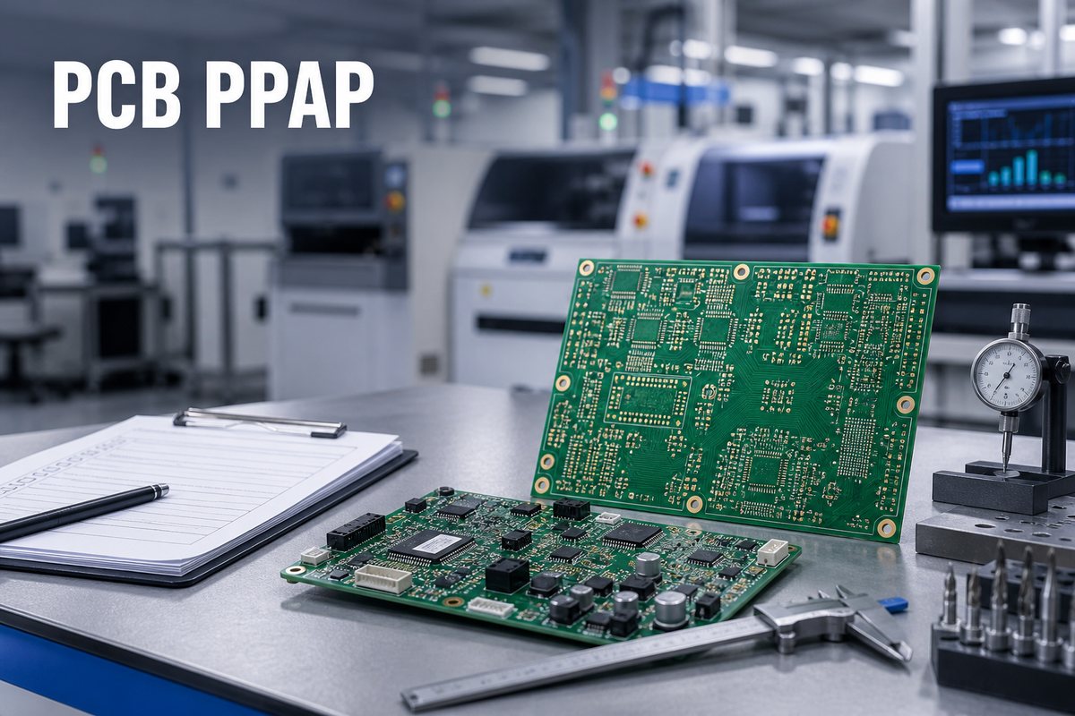
PCB PPAP applies the production part approval process PPAP to a PCB or PCBA so buyers can approve more than a sample that happens to pass inspection. The submission should show that the agreed board revision, materials, manufacturing process, inspection plan and production records can repeatedly meet the customer’s requirements. If the required evidence is not defined before quotation, approval can be delayed by missing documents, unplanned testing, unclear responsibilities or a production change that was never submitted for review.
EBest Circuit (Best Technology) helps customers connect PPAP requirements with PCB fabrication, component sourcing, PCBA assembly, testing and traceability. In the first half of 2026, our engineering team delivered 18 completed PPAP reports, giving customers structured production evidence for PCB approval and traceability. This practical experience helps customers define the required submission before production, keep manufacturing evidence connected to the correct revision and move from approval samples to repeat orders with fewer documentation gaps.
What Is the Production Part Approval Process PPAP?
The production part approval process PPAP is used to confirm that a supplier understands the engineering design record and specification requirements and that the planned production process can consistently make conforming parts under actual production conditions.
For a PCB or PCBA buyer, PPAP is therefore not just a folder of forms. It is a decision package used to answer whether the supplied part is ready for production approval.
A useful PCB PPAP submission should help the customer confirm:
The correct PCB, BOM and assembly revisions were used.
Materials, components and approved sources match the agreed requirements.
The production process is defined and controlled.
Measurements and test results meet the acceptance criteria.
Samples came from a representative production process.
Material, process and inspection records can be traced to the delivered batch.
Future changes will be reviewed before they affect approved production.
The customer or authorized approval organization decides whether the submission is approved. The PCB or PCBA supplier prepares the manufacturing evidence within its agreed scope; it does not replace the customer’s product-design responsibility, system validation or final approval authority.
What Must PCB PPAP Prove Before Production?
PCB PPAP must connect the approved product definition to a repeatable manufacturing process. A visually acceptable sample is not enough if the supplier cannot show which revision, material lot, process settings and inspection results produced it.
Before production approval, buyers should be able to answer five questions:
Was the correct product built? The Gerber data, drawing, stack-up, BOM, CPL, firmware or programming instructions and other controlled files must use the approved revision.
Were the correct materials and components used? Laminate, copper weight, surface finish, solder mask, components and approved substitutions must match the agreed specification.
Can the manufacturing process repeat the result? Fabrication, stencil, SMT, through-hole, reflow, wave soldering, coating, programming and testing requirements must be translated into controlled production instructions where applicable.
Does the product meet the measurable requirements? Dimensional, electrical, soldering, cleanliness, functional or reliability results should be matched to the customer’s acceptance criteria.
Can the evidence be traced? The supplier should be able to connect the sample and report to the relevant order, material batch, production route and inspection record.
This is why PPAP should be discussed before the approval build. Adding a special study, customer form, third-party test or traceability requirement after production may require new samples or a repeat production run.
Which PPAP Documents Should Come From Your PCB Supplier?
The AIAG PPAP framework contains 18 potential elements, but that does not mean every PCB supplier automatically owns every element or that every submission requires the same package. The customer should define the required level, customer-specific forms and responsibility for each item.
The most practical approach is to separate customer-controlled inputs from supplier manufacturing evidence.
Responsibility
Typical information or evidence
Customer or design owner
Approved drawing and design record, revision, specifications, special characteristics, application requirements, acceptance criteria and customer-specific forms
PCB/PCBA supplier
Process flow, manufacturing instructions, applicable PFMEA and control plan, material records, dimensional results, electrical or assembly inspection results, initial samples and batch traceability within the agreed scope
Customer and supplier to confirm
Part Submission Warrant ownership, MSA or capability studies, laboratory requirements, IMDS submission, component sub-tier evidence, master sample, checking aids and retention period
For an efficient quotation, ask the supplier to identify each requested item as:
Included in the quoted PPAP scope.
Available from an existing manufacturing record.
Requiring a dedicated production study or sample run.
Requiring an approved external laboratory or sub-tier supplier.
Supplied or approved by the customer.
Not applicable to the PCB or PCBA project.
This prevents a common commercial problem: both parties agree to “PPAP,” but the customer expects a complete customer-specific package while the quotation covers only samples and basic inspection reports.
How Do PPAP Levels Change What Your Supplier Submits?
The PPAP submission level controls what is sent to the customer and what must remain available for review. It does not change the underlying obligation to manufacture the approved part consistently.
PPAP level
General submission expectation
Level 1
Part Submission Warrant only
Level 2
Warrant, product samples and limited supporting data
Level 3
Warrant, product samples and complete supporting data
Level 4
Warrant and other requirements defined by the customer
Level 5
Warrant, samples and complete supporting data available for review at the supplier’s manufacturing location
Level 3 is frequently requested in automotive supply chains, but it should not be treated as the automatic requirement for every PCB or PCBA. The customer must specify the submission level and any customer-specific additions.
Before accepting a level, confirm:
The exact document list and form revision.
Whether evidence is submitted, retained or reviewed on site.
The required sample quantity and production-run conditions.
Which special characteristics require capability evidence.
Whether sub-tier PCB, component or laboratory records are required.
The target submission date and review cycle.
A clear level definition makes the supplier’s quotation more accurate and reduces the risk of discovering additional work immediately before approval.
PPAP vs FAI: What Is Different for PCB Approval?
PPAP and first article inspection both use measured evidence, but they answer different questions.
Approval method
Main question
FAI
Does the first manufactured item conform to the drawing and specified characteristics?
PPAP
Can the defined production process repeatedly manufacture conforming parts and maintain the required evidence?
An FAI report may be part of the evidence used during PCB qualification, but dimensional conformity alone does not establish the full production-control picture expected from PPAP.
PCB PPAP may extend beyond FAI by connecting the results to:
Process flow and production controls.
Material and component traceability.
Risk analysis and control planning where required.
Measurement-system or process-capability evidence for specified characteristics.
Sample origin and representative production conditions.
Change notification and resubmission requirements.
The customer should still define whether it needs FAI, PPAP or both. Treating the terms as interchangeable can leave important evidence missing from the approval package.
When Do PCB Changes Require a New PPAP Submission?
An approved sample does not give unrestricted permission to change the product or process. A change may alter electrical performance, reliability, solderability, fit, traceability or long-term repeatability even when the finished board looks similar.
Changes that should be reviewed against the customer’s PPAP rules include:
PCB drawing, Gerber, stack-up or specification revision.
Laminate, copper, solder mask, surface finish or other material change.
BOM revision or component substitution.
Change of an approved material or component source.
New tooling, stencil, fixture or manufacturing equipment.
Significant change to fabrication, assembly, coating, programming or test methods.
Transfer to another production line, factory or sub-tier supplier.
Restart after an extended production interruption.
Correction following a nonconformance that changes the approved process.
The existence of a change does not automatically determine the required submission level. The supplier should notify the customer with enough information for the customer to decide whether approval, limited evidence or a complete resubmission is required.
For PCB and PCBA programs, revision control is especially important because one commercial part number may involve several connected files. Gerber data, BOM, CPL, assembly drawings, test instructions and firmware references must remain aligned.
What Should Be Confirmed Before a PCB PPAP Quote?
A PCB PPAP quotation should make the approval work visible. Quoting only the board or assembly price leaves both parties exposed to extra samples, testing fees, engineering time and schedule changes later.
Send the following information with the RFQ:
Approved Gerber data, drawing and revision.
BOM and CPL for PCBA projects.
Required PPAP level and customer-specific checklist.
Sample quantity and expected production-run quantity.
Special characteristics and acceptance limits.
Required dimensional, electrical, functional or reliability tests.
Required forms, language and file format.
IMDS, material declaration or sub-tier evidence requirements.
Required laboratory accreditation, if applicable.
Submission date and planned production-approval date.
Change-notification and document-retention requirements.
The supplier’s quotation should then clarify:
Which PPAP documents are included.
Which tests are performed internally or externally.
Whether a dedicated production run is required.
Sample, tooling, fixture and laboratory charges.
Expected preparation and review schedule.
Information still required from the customer.
This gives the buyer a usable approval plan instead of a low initial price followed by unplanned documentation charges and delayed production.
How Does EBest Support PCB PPAP Evidence?
EBest Circuit (Best Technology) supports PCB fabrication, component sourcing, PCBA assembly, inspection and customer-defined testing coordination through one project path. Our IATF 16949 quality-management capability and engineering experience provide a practical foundation for automotive and other controlled-production projects.
Our engineering department completed 18 PPAP reports in the first half of 2026. During the same period, the team also prepared IQ, OQ and PQ reports for five products, created 332 new SMT programs and maintained 489 product and process records in MES. These are not presented as identical PPAP packages; they demonstrate active experience in converting customer requirements into controlled manufacturing and supporting records.
Depending on the confirmed project scope, EBest can coordinate:
Pre-production review of PCB, BOM, CPL, drawings and special requirements.
DFM review and engineering questions before the approval build.
Process flow, manufacturing instructions, SOPs and control records.
First-article and trial-production issue review.
Material, order and product-batch traceability through MES.
Incoming, in-process and outgoing inspection records.
Electrical, AOI, X-ray, functional or other agreed testing.
Component sourcing and approved-substitution control.
PCB fabrication, PCBA assembly and repeat production.
Our MES records can connect incoming materials, warehouse activity, production stages, inspection and shipment to the relevant order or product record. This helps customers investigate a question without separating the approval sample from the manufacturing history that produced it.
For each new project, EBest first reviews the customer’s requested PPAP level, document list, special characteristics and testing requirements. We then identify what can be supplied from our manufacturing scope, what requires a dedicated study or third party, and what must come from the customer. This prevents a certification or approval promise from being made before the evidence has been defined.
FAQs About Production Part Approval Process PPAP
Is PPAP required for every PCB or PCBA?
No. PPAP is commonly associated with automotive and other controlled supply chains, but the customer determines whether it is required. Many industrial, medical or high-reliability buyers may request similar evidence without using the complete AIAG PPAP format.
Is PCB PPAP a separate AIAG standard?
No. PCB PPAP is the production part approval process applied to a PCB or PCBA supplied part. The applicable submission requirements still come from the customer’s PPAP manual and customer-specific requirements.
Is Level 3 PPAP always required for automotive PCBs?
No. Level 3 is frequently requested, but it is not a universal default for every program. The customer must define the submission level and any additional documents.
What is a Part Submission Warrant?
The Part Submission Warrant, or PSW, summarizes the submitted part and records the supplier’s declaration that the applicable PPAP requirements have been met. The required format and signature responsibility should be confirmed with the customer.
Can an FAI report replace PPAP?
Not automatically. FAI primarily confirms that an initial item meets specified characteristics. PPAP addresses the broader ability of the production process to make conforming parts consistently. The customer decides whether FAI, PPAP or both are required.
Does a BOM substitution require PPAP resubmission?
It may. A component substitution can affect fit, function, reliability, compliance, sourcing approval and test results. The proposed change should be submitted to the customer before use, and the customer should decide the required approval evidence.
How early should PPAP requirements be discussed?
They should be defined before quotation and before the approval build. Early confirmation allows the supplier to include the correct samples, production conditions, studies, records, third-party tests and schedule.
Can EBest provide a complete Level 3 PPAP package?
EBest has practical PPAP-report experience, including 18 reports completed in the first half of 2026. However, the exact package depends on the customer’s checklist, product scope and responsibility allocation. We review every requested element before confirming the deliverables.
Need manufacturing evidence that stays connected to your approved PCB revision and repeat production? Send your Gerber files, drawings, BOM/CPL, PPAP level, document checklist, sample quantity and testing requirements to sales@bestpcbs.com. EBest Circuit will review the requested scope and help you prepare a clear quotation and approval plan for your PCB PPAP project.
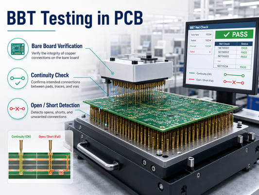
BBT testing in PCB manufacturing is used to verify whether the copper network is correctly connected before the boards move into assembly. By detecting open circuits, short circuits, and unwanted electrical connections, BBT helps prevent defective boards from entering PCBA production.
For PCB projects that require stable quality control, EBest Circuit supports bare PCB manufacturing and PCBA assembly with electrical testing, AOI inspection, X-ray inspection, and traceable quality processes. Customers can provide Gerber files, layer information, copper thickness, surface finish requirements, and production quantities to receive an engineering review and quotation guidance through sales@bestpcbs.com.
What Is BBT Testing in PCB?
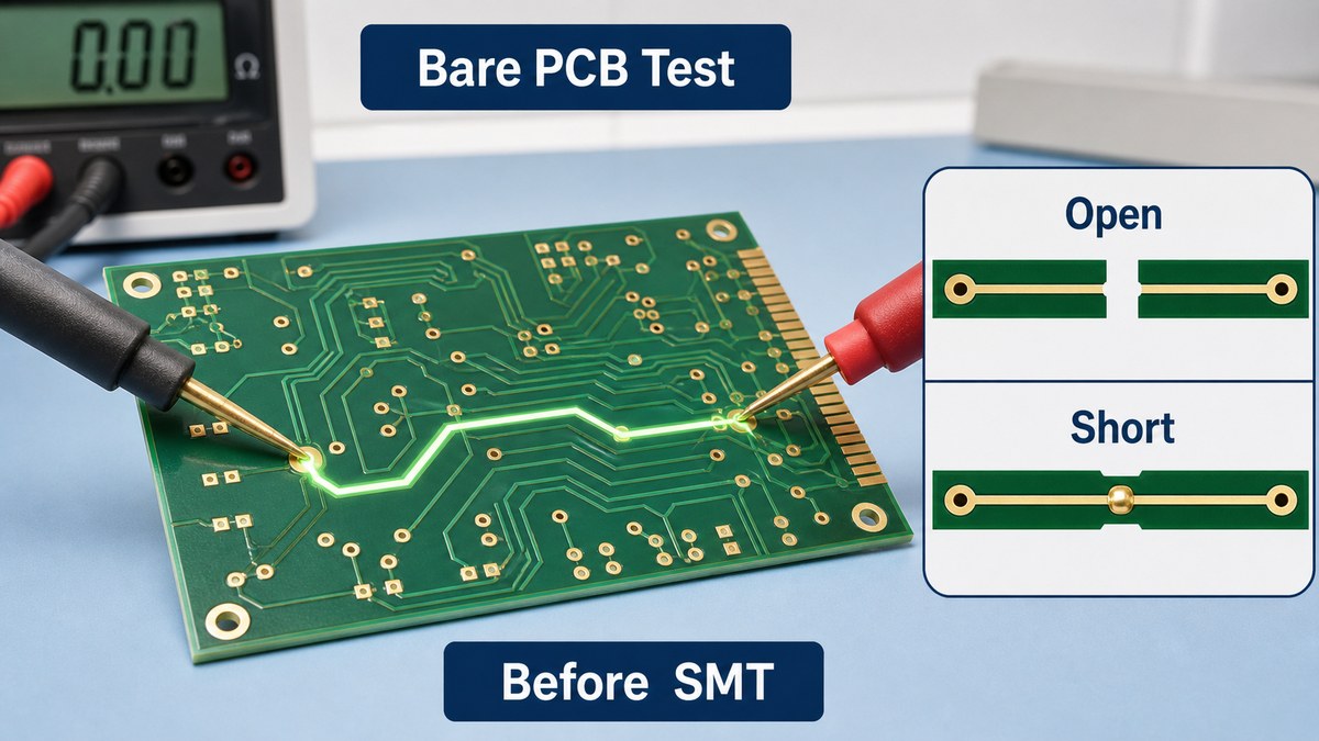
BBT testing stands for Bare Board Testing. It is a form of bare board PCB testing performed on a completed PCB before components are assembled. The purpose is to confirm that all designed conductive paths match the PCB data and that there are no unwanted electrical failures.
During BBT testing, test probes contact specific points on the PCB surface, and the system checks whether each circuit connection meets the expected electrical conditions.
A typical BBT system verifies:
Open circuits caused by broken traces or incomplete plating
Short circuits between adjacent copper paths
Incorrect connections caused by manufacturing defects
Continuity problems in multilayer PCB structures
Unlike visual inspections such as AOI, BBT does not inspect the physical appearance of traces. It verifies the actual electrical performance of the finished board.
For multilayer, HDI, fine-pitch, and high-density PCB designs, BBT becomes especially valuable because many defects cannot be reliably identified through visual inspection alone.
Why Is BBT Testing Required for PCB Manufacturing?
PCB manufacturing involves multiple processes that can affect electrical connections, including imaging, etching, lamination, drilling, and copper plating. Even small process variations can create electrical failures that are difficult to detect without testing.
BBT testing is required because it provides a final electrical verification before PCB assembly.
Common reasons manufacturers perform BBT include:
Purpose
Engineering Value
Detect open circuits
Prevents broken signal or power paths
Detect shorts
Avoids unexpected current paths and board failure
Verify circuit continuity
Confirms the PCB matches the original design
Improve assembly yield
Reduces defective boards reaching SMT production
For customers purchasing assembled boards, detecting PCB defects before component placement is usually more cost-effective. A faulty bare board can cause additional losses from component usage, assembly labor, and functional testing.
How Does BBT Testing Work?
The BBT testing process compares the manufactured PCB against the original electrical design data, usually generated from Gerber or ODB++ files.
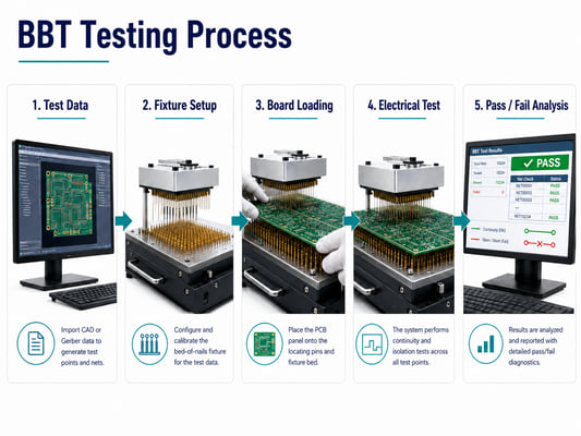
The general workflow includes the following steps:
Test data preparation The PCB test system imports design files and identifies electrical nets, test points, and expected connections.
Test fixture preparation A fixture with test probes is created according to the PCB structure. Each probe contacts specific pads or vias on the board.
PCB loading and positioning The bare PCB is placed into the testing equipment with accurate alignment.
Electrical measurement The tester applies electrical signals to verify continuity and isolation between different circuits.
Result evaluation The system compares measured results with the design database and identifies defective locations if failures occur.
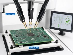
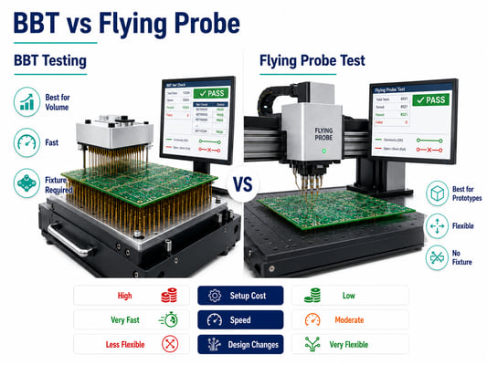
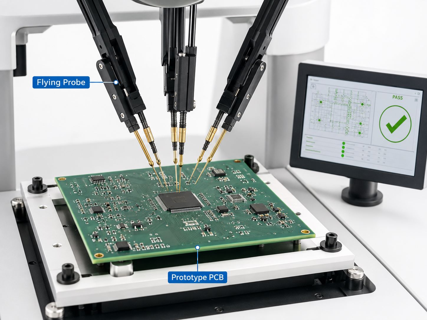
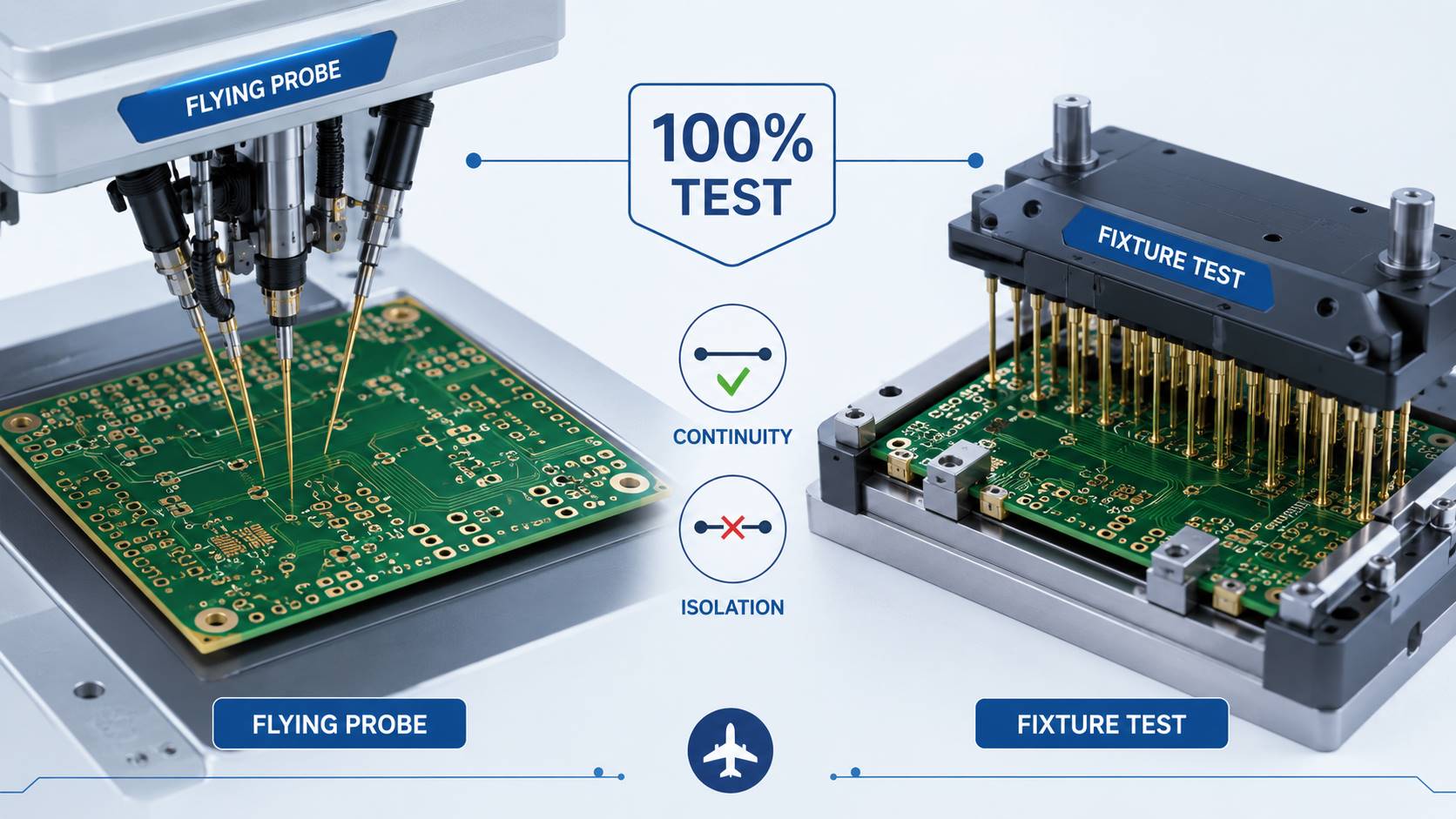
For high-volume production, fixture-based BBT is widely used because it offers fast testing speed and repeatable results. For prototypes or low-volume orders, manufacturers may choose flying probe testing because it avoids fixture costs.
What Is the BBT Testing Procedure in PCB Manufacturing?
A PCB BBT test normally starts after the PCB fabrication process is completed. The exact sequence may vary depending on the factory process flow and customer requirements.
A typical procedure includes:
Step
Operation
Purpose
1
Import PCB test data
Define electrical networks
2
Prepare testing fixture
Ensure probe contact accuracy
3
Load PCB panels
Position boards for testing
4
Perform electrical test
Check continuity and insulation
5
Analyze test results
Separate qualified and failed boards
Before testing begins, manufacturers usually confirm:
Correct Gerber or ODB++ data
PCB revision consistency
Test point accessibility
Required test coverage level
For complex multilayer PCBs, proper test preparation is important because insufficient test points or incorrect data mapping can reduce testing effectiveness.
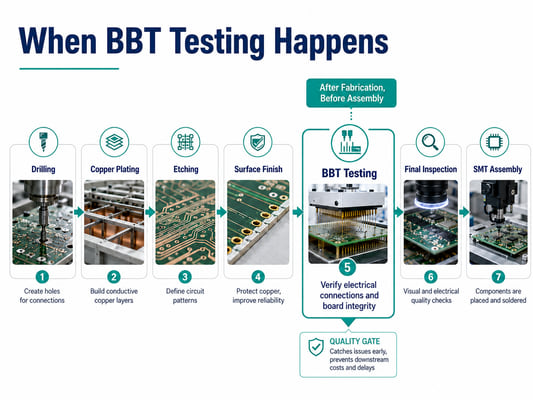
When Does BBT Testing Start During PCB Production?
BBT testing starts after PCB fabrication is completed and before PCB assembly begins.
BBT testing focuses on electrical failures that affect PCB functionality. It is especially effective for identifying hidden connection problems inside complex PCB structures.
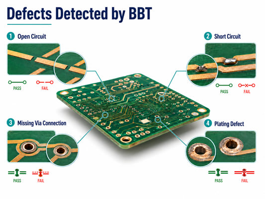
Common defects detected by BBT include:
Open circuits caused by broken copper traces
Short circuits between different electrical nets
Missing connections between layers
Incorrect via connections
Plating-related continuity problems
However, BBT does not replace every inspection method. For example:
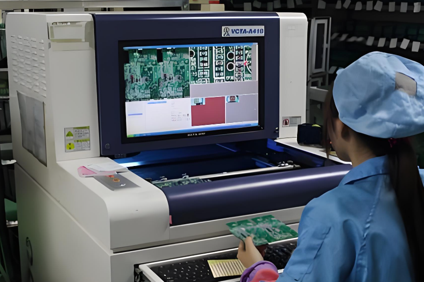
AOI checks physical defects such as trace shape, solder mask issues, and missing copper patterns.
X-ray inspection checks internal structures such as hidden solder joints or vias.
BBT confirms electrical connectivity.
A reliable PCB quality system usually combines multiple inspection methods based on product requirements.
What Types of PCB Require BBT Testing?
Most professional PCB manufacturers recommend electrical testing for boards where reliability and circuit density are important.
Common applications include:
Multilayer PCBs
HDI PCBs
High-frequency RF PCBs
Automotive electronics
Medical equipment boards
Industrial control systems
Power electronics PCBs
The need for BBT depends mainly on:
PCB complexity
Production quantity
Reliability requirements
Cost of failure after assembly
For simple single-sided boards with low-risk applications, customers may use different inspection strategies. However, for multilayer boards used in critical electronics, BBT is generally considered a standard quality step.
How Much Does PCB BBT Testing Cost?
The BBT testing cost is not a fixed amount because it depends on PCB design, production volume, and testing requirements.
The main factors affecting cost include:
Factor
Cost Impact
PCB size
Larger boards require larger fixtures and more testing resources
Layer count
Complex designs require more test points and verification
Production quantity
High volume reduces average testing cost
Fixture requirement
Custom fixtures increase initial setup cost
Test coverage
Higher coverage requires more testing time
For mass production, fixture-based BBT usually provides a lower cost per board because the testing speed is high.
For prototypes, low-volume orders, or frequent design changes, flying probe testing may be more practical because no dedicated fixture is required.
When requesting a quotation, customers should provide:
PCB dimensions
Layer count
Gerber or ODB++ files
Production quantity
Required test method
Expected delivery schedule
These details allow manufacturers to evaluate the most suitable testing solution.
Flying Probe Test vs BBT: What Is the Difference?
The choice between BBT and flying probe testing mainly depends on production volume, lead time, and cost structure.
Item
BBT Testing
Flying Probe Testing
Main application
Medium and high-volume production
Prototype and low-volume production
Fixture requirement
Requires dedicated fixture
No dedicated fixture needed
Testing speed
Faster for mass production
Slower due to probe movement
Initial setup cost
Higher
Lower
Design changes
Requires fixture updates
Easier for frequent changes
For customers producing thousands of PCBs, BBT is usually more economical because the fixture investment is distributed across many boards.
For prototypes or engineering samples where the design may change frequently, flying probe testing often provides better flexibility.
How Do PCB Manufacturers Ensure Reliable BBT Testing Results?
Reliable BBT testing depends on more than having testing equipment. The accuracy of the final result also depends on data preparation, equipment maintenance, and process control.
Important factors include:
Accurate test data generated from the latest PCB design revision
Proper fixture maintenance and probe condition checks
Controlled testing parameters
Clear failure analysis procedures
Production traceability
At EBest Circuit, PCB projects are supported by engineering review, fabrication control, and inspection processes including electrical testing, AOI, and PCBA verification. This helps customers evaluate manufacturing risks before moving into volume production.
For projects with tight reliability requirements, customers should confirm:
Testing standard
Test coverage requirement
Inspection reports needed
Traceability expectations
FAQs About BBT Testing in PCB
What does BBT stand for in PCB?
BBT stands for Bare Board Testing. It is an electrical test used to verify PCB connectivity before component assembly.
Is BBT testing included in PCB manufacturing?
Many PCB manufacturers include basic electrical testing as part of their production process, but customers should confirm whether BBT is included in the quotation.
What is the difference between BBT and flying probe testing?
BBT uses a dedicated fixture and is suitable for volume production, while flying probe testing uses moving probes and is more flexible for prototypes.
Can BBT testing detect PCB open and short circuits?
Yes. BBT is mainly used to detect open circuits, short circuits, and other electrical connection failures.
How long does PCB BBT testing take?
Testing time depends on PCB size, design complexity, test coverage, and production quantity. High-volume production usually benefits from faster fixture-based testing.
Conclusion
BBT testing in PCB manufacturing is an important electrical verification step that confirms whether a bare PCB meets the intended circuit design before assembly. Understanding the BBT testing process, testing procedure, timing, and cost factors helps engineers and purchasing teams choose the right manufacturing approach.
For PCB projects requiring reliable electrical performance, EBest Circuit provides PCB and PCBA manufacturing support with engineering communication, quality inspection, and production testing capability. Send your Gerber files, PCB specifications, and production requirements to sales@bestpcbs.com for engineering review and quotation support.
A solder float test PCB evaluation requires a production-representative coupon, controlled molten-solder exposure, and PTH inspection against an invoked acceptance specification. A record that says only “288°C for 10 seconds, pass” omits moisture conditioning, solder contact, exposure count, hole construction, section location, and the disposition criterion.
The test creates a steep temperature gradient from the solder-contact face into the laminate. Copper and the resin-glass system expand differently, so marginal barrel plating, corner geometry, internal-layer connections, and laminate interfaces can open or separate.
What Is a Solder Float Test for PCB?
A PCB solder float test places a prepared bare-board specimen on molten solder for a specified dwell so that the solder-contact face receives rapid conductive heating. For plated-through-hole thermal stress, the specimen is subsequently microsectioned. The section exposes the copper barrel, knee or corner regions, lands, resin, glass reinforcement, and inner-layer connections that cannot be judged from the exterior surface.
The mechanism is more severe than the temperature number alone suggests. The solder-facing copper heats first while the upper portion of the coupon lags. Through-thickness expansion of the laminate loads the comparatively low-expansion copper barrel in tension. At a plated-hole corner, the load is concentrated where barrel copper changes direction into the surface land. At an inner-layer junction, local resin geometry and copper continuity determine whether the connection remains intact.
IPC-TM-650 Method 2.6.8E is an established method for evaluating the ability of plated-through holes to withstand extreme heat encountered during assembly, rework, or repair. It is a test method, not a universal product acceptance table. The drawing, procurement specification, applicable IPC-6010-series performance specification, or customer requirement must still define the class, sampling, permitted conditions, and disposition criteria.
What Does a Solder Float Test Evaluate?
For structural thermal stress, the test evaluates whether plated-through holes, lands, internal connections, and surrounding laminate remain acceptable after the specified rapid heat exposure. It is most useful for revealing weaknesses that are dormant at room temperature but open when the laminate expands or when moisture becomes vapor.
The evidence can support four narrow decisions. First, did the tested barrel copper remain continuous? Second, did the copper-to-inner-layer connection remain intact? Third, did lands and foil remain attached without prohibited lifting or cracking? Fourth, did the laminate remain free from prohibited blistering, delamination, or other heat damage?
A pass does not establish component solder-joint reliability, field thermal-cycle life, or survival through every lead-free reflow profile. Solder float heating is one-sided and extremely rapid. Convection reflow heats the board from both sides through a time-temperature profile, while environmental cycling repeatedly changes the entire assembly temperature. These different temperature fields create different strain histories.
Required Decision
Relevant Evidence
Evidence Not Supplied
PTH survival after the invoked solder-float condition
Representative coupon, controlled exposure, and conforming microsection
Long-term field life
Surface-finish wetting
Wetting coverage and dewetting observations from a solderability method
Internal barrel integrity
Survival of the intended reflow process
Assembly simulation using the intended profile and number of excursions
Established by solder float alone
Reliability of assembled solder joints
Assembly-level cycling, monitoring, and failure analysis
Established by a bare-board coupon
Which Standards Apply to PCB Solder Float Testing?
The correct standard depends on whether the decision concerns PTH thermal integrity, flexible-material resistance, reflow simulation, or termination solderability. Using a solder pot does not make these methods interchangeable.
Document or Method
Controlled Scope
Engineering Use
IPC-TM-650 2.6.8E
Thermal stress of plated-through holes
Conditioning, solder-float exposure, and subsequent microsection evaluation
IPC-TM-650 2.6.27
Convection-reflow assembly simulation
Closer representation of an intended surface-mount reflow profile
IPC-TM-650 2.4.13F
Solder-float resistance of flexible printed wiring materials
Material evaluation within the method’s stated flexible-circuit scope
J-STD-003
Solderability of printed boards
Wetting acceptance for designated board terminations
Applicable performance or customer specification
Product acceptance
Class, sample quantity, allowed defects, and lot disposition
A test plan should state the document number, revision, condition, number of exposures, and acceptance document. Writing only “IPC solder float” leaves the laboratory to choose among different purposes and conditions. That ambiguity becomes especially serious when a supplier interprets the request as a wetting test while the customer expects a microsectioned PTH thermal-stress result.
Increasing the number of solder-float exposures does not reproduce a convection-reflow profile. Qualification must match the product’s heat-transfer mode, temperature history, and expected failure mechanism.
How Should PCB Samples Be Prepared Before a Solder Float Test?
Sample preparation must control moisture, confirm coupon representation, and document a defect-free baseline before the specimen touches solder. Otherwise, the laboratory cannot distinguish a manufacturing defect from conditioning damage or test handling.
For the referee procedure in IPC-TM-650 2.6.8E, specimens are dried for a minimum of six hours at 121–149°C and cooled in a desiccator. That conditioning removes uncontrolled moisture as a test variable. It should not be silently substituted when the purchase requirement calls for an as-received or moisture-preconditioned evaluation, because drying can suppress moisture-driven delamination that the customer intended to assess.
Match the coupon to the production board’s thickness, layer count, material designation, surface finish, finished and drilled hole diameters, copper weights, plating process, and inner-layer connection pattern. Record the material lot when available. High aspect-ratio holes, small finished diameters, heavy copper distribution, and resin-starved local constructions may experience more strain than an easier coupon.
Inspect and photograph the specimen before exposure. Reject or separately document pre-existing blisters, land damage, plugged holes, contamination, edge damage, or suspected delamination. If continuity monitoring is required, record the baseline resistance and measurement path. The laboratory should also identify which holes will be sectioned so that convenient, visually clean holes are not selected only after the test.
Apply the flux required by the method to the plated holes and relevant specimen surface. Flux quantity and coverage affect wetting and therefore the consistency of thermal contact. Excess residue can also conceal surface evidence. The preparation record should state the flux identification, lot or expiration control where required, application method, and any permitted preheat.
How Is a Solder Float Test for PCB Performed?
The procedure verifies bath condition, places the prepared specimen on a clean solder surface for the timed dwell, removes it without shock, cools it as specified, and transfers it to controlled inspection. Each step affects the actual thermal load.
Stabilize and verify the bath. Confirm the required solder composition and temperature at the specified measurement location. A controller display does not prove that the contact surface is within tolerance.
Prepare a clean contact surface. Remove dross as permitted by the procedure. Oxide or dross can hold part of the coupon above the liquid solder and create uneven heating.
Flux the specified areas. Use the required flux and application method. Do not add an unapproved preheat or extended activation time.
Start consistent contact. Lower the specimen flat onto the molten solder without forcing it below the surface. The timing reference must be consistent from specimen to specimen.
Control the dwell. IPC-TM-650 2.6.8E specifies a ten-second exposure with a +1/-0 second tolerance for its listed conditions. The invoked requirement controls the actual test.
Remove without mechanical damage. Do not bend, shake, scrape, or shock the specimen while the solder remains liquid. Mechanical loading at that moment can create damage that is not attributable to thermal stress alone.
Cool and repeat only as specified. Record cooling time and method between exposures. An unrecorded hot restart changes the starting temperature and accumulated strain.
Clean, inspect, and section. Preserve visible evidence before destructive preparation. Maintain traceability between the specimen, photographed surface, selected holes, and finished microsection.
The operator should record the actual bath temperature and dwell for each exposure, not only the nominal recipe. If a specimen rocks, traps gas, loses full contact, or is accidentally pushed into the bath, mark the run invalid and repeat with a new qualified specimen rather than averaging the event into a pass.
Which Parameters Control Solder Float Test Severity?
Severity is determined by the combined temperature, dwell, starting condition, contact quality, exposure count, cooling history, specimen geometry, and material response. Two laboratories can use the same nominal bath temperature and produce different stress when these other variables are uncontrolled.
Parameter
Effect on the Specimen
Control or Record
Bath temperature
Changes heat flux and peak temperature reached during the dwell
Actual value, tolerance, probe location, and verification time
Dwell time
Changes heat penetration and copper-laminate strain
Actual time for every exposure and timing reference
Starting temperature and moisture
Changes thermal gradient and vapor-pressure contribution
Drying, storage, desiccator cooling, and preconditioning history
Solder contact
Controls whether heating is uniform across the face
Dross removal, flat placement, flux coverage, and anomaly notes
Exposure count and cooling
Changes accumulated damage and recovery between events
Number of passes, interval, cooling method, and restart temperature
Coupon construction
Changes strain concentration and heat flow
Thickness, layer count, hole geometry, plating, copper distribution, and material
Method 2.6.8E lists Condition A at 288±5°C, Condition B at 260±5°C, and Condition C at 232±5°C. These are method conditions, not a menu from which the laboratory should pick the most convenient value. The procurement document must invoke the condition or provide the governing product requirement.
A higher temperature cannot compensate for poor process definition. A short exposure at 288°C and a longer exposure at 260°C do not necessarily create equivalent strain because the heating rate, peak temperature distribution, resin response, and interfacial stress differ. Equivalence requires validated correlation for the construction, not a simple temperature-time trade.
What PCB Defects Can a Solder Float Test Reveal?
The test can reveal thermally activated cracks and separations in the PTH structure, lands, internal connections, and laminate. The defect name alone is insufficient; location, orientation, extent, and connection to the functional conductor determine the risk.
Barrel cracking: a circumferential or partial crack through the plated copper wall. It may open under expansion and close again after cooling, so a room-temperature continuity check can miss it.
Corner or knee cracking: a crack at the transition from barrel copper to the surface land. The geometric change concentrates strain, particularly when copper thickness or local plating geometry is marginal.
Inner-layer connection separation: loss of intimate connection between the plated barrel and an internal copper feature. Sectioning must pass through the relevant connection; a nearby plane can miss the discontinuity.
Land lifting or land separation: upward movement or separation of a surface land from the laminate. Distinguish true thermally induced lifting from damage introduced during section preparation.
Foil cracking: cracking in surface or internal copper adjacent to the hole. Record whether the crack reaches a functional conductor.
Blistering: a localized raised area caused by separation or volatile pressure beneath a surface layer. Photograph it before grinding destroys the external evidence.
Delamination: separation between laminate plies or at another interface. Report its location, length, relationship to conductors, and whether it was present before exposure.
Resin recession or resin damage: changes around the hole wall that must be judged using the invoked specification and preparation quality rather than an improvised limit.
Failure morphology guides the investigation but does not prove a single root cause. Barrel or corner cracks may direct attention to plating thickness, copper ductility, hole preparation, geometry, and laminate expansion. Delamination may require review of moisture history, lamination bonding, resin distribution, material compatibility, and the validity of the exposure. A corrective action should not be assigned until the defect is confirmed in representative sections and correlated with manufacturing records.
How Should PCB Solder Float Test Results Be Inspected?
Inspect the specimen in a fixed sequence so each internal finding remains traceable to its pre-test condition and coupon location. Cleaning, cutting, or etching out of sequence can destroy evidence needed for disposition.
Preserve the surface condition. Photograph the specimen before cleaning or cutting. Record blistering, land movement, discoloration, surface damage, solder obstruction, and handling anomalies.
Repeat required electrical checks. Compare continuity or resistance with the baseline. Stable room-temperature continuity does not exclude a crack that opened only while hot.
Select holes without bias. Use locations defined by the test plan or a documented random method. Inspecting only the cleanest or worst-looking hole can distort the lot decision.
Cut near the hole centerline. An off-center section can exaggerate plating thickness, omit an inner-layer connection, or hide a partial barrel crack.
Examine the as-polished section. Check barrel and corner cracks, land separation, voids, laminate separation, and plating continuity before etching changes the contrast.
Microetch only when required. Use the etched condition to clarify copper interfaces and boundary detail; retain both views because etched and as-polished images are not interchangeable.
Confirm isolated findings. Prepare another plane or serially grind when a suspected defect appears in only one section. Do not assign a lot-wide root cause from one ambiguous feature.
Separate artifacts from defects. Check whether edge rounding, pullout, scratches, smearing, or overetching created the observed feature.
Document the disposition. Record the coupon and hole location, magnification, scale, defect orientation, image condition, and exact acceptance clause.
How Does the Solder Float Thermal Stress Test Differ from a Solderability Test?
Structural solder-float testing asks whether the PCB construction survives rapid heating; solderability testing asks whether specified metallic terminations wet with solder. Both can use molten solder, but they inspect different objects and produce different acceptance evidence.
Decision Element
Structural Solder Float
Solderability Test
Primary question
Did the PTH and laminate remain structurally acceptable?
Did the designated surface wet as required?
Primary observation
Microsectioned barrel, lands, interfaces, and laminate
Wetting coverage, nonwetting, and dewetting
Typical concern
Cracking, separation, blistering, or delamination
Oxidation, finish condition, contamination, or poor wetting
Applicable method family
Thermal-stress and product-performance requirements
J-STD-003 or another invoked solderability procedure
A board can wet well and still contain a thermally damaged barrel. It can also retain sound internal structure while an aged or contaminated surface finish wets poorly. If both risks matter, specify both tests and keep their sample preparation and acceptance records separate. A PCB solderability test should not be reported as PTH thermal-stress evidence.
How Does Solder Float Testing Differ from Thermal Cycling and Thermal Shock?
Select the method by heat-transfer mode, repetition, monitored object, and required reliability decision. Solder float is not a faster substitute for a chamber-based qualification.
Comparison
Solder Float
Thermal Cycling
Thermal Shock
Heat input
Rapid conductive heating from the solder-contact face
Controlled chamber heating and cooling of the whole specimen
Rapid transfer between hot and cold environments
Exposure pattern
One or more short method-defined dwells
Repeated ramps, dwells, and cycles
Repeated abrupt temperature transitions
Primary stress
Steep through-thickness gradient and PTH strain
Cyclic expansion and fatigue accumulation
High strain rate from rapid environmental change
Typical test object
Bare-board coupon or representative PCB specimen
Bare board or assembled product with monitoring
Board, assembly, material, or component as specified
Best use
PTH and laminate response to rapid assembly-like heat
Fatigue and intermittent opens over repeated temperature excursions
Resistance to abrupt temperature change
Key limitation
Does not reproduce a chamber profile or field cycling
Does not reproduce direct molten-solder contact
May be more abrupt than the intended operating environment
Use convection-reflow simulation when the intended assembly profile must be represented. Use a broader PCB thermal stress test plan when repeated environmental transitions, solder-joint fatigue, or monitored field reliability is the required decision.
What Should a PCB Solder Float Test Report Include?
A defensible report must allow another qualified laboratory to identify the same specimen, reproduce the exposure, inspect equivalent locations, and apply the same acceptance rule. A pass/fail certificate without this chain is weak procurement evidence.
Requirement: test method, revision, condition, applicable performance specification, class, customer deviations, sample quantity, and acceptance clause.
Specimen identity: part number and revision, panel or coupon identity, lot, material and construction, board thickness, layer count, hole type and size, and relevant plating information.
Conditioning: drying or moisture preconditioning, temperature and duration, storage after conditioning, desiccator use, and elapsed time before testing.
Bath controls: solder alloy, flux, bath setpoint and actual verification, measurement location, surface preparation, and equipment identification or calibration status as required.
Exposure record: actual dwell, number of passes, cooling interval and method, specimen orientation, contact anomalies, and operator observations.
Inspection evidence: pre- and post-test photographs, electrical results when required, section map, evaluated hole locations, as-polished and etched images, scale, magnification, and defect annotations.
Disposition: result for each specimen, exact acceptance clause, nonconformance description, reviewer, and authorization of the final report.
Procurement teams should reject ambiguous substitutions. If the purchase order invokes Condition A and microsection evaluation, a supplier should not close the requirement with a wetting photo, an unsectioned coupon, or a certificate that omits the actual condition. Any deviation should be approved before testing, not explained after a failed lot.
What Can Make Solder Float Test Results Misleading?
Results become misleading when coupon representation, moisture history, real bath contact, timing, cooling, or section selection differs from the stated test. These controls can produce false confidence or false rejection even when the nominal temperature is correct.
Unrepresentative coupons: easier holes or a different material construction can hide the production board’s highest-strain feature. Compare coupon design and panel location with the actual stackup.
Uncontrolled moisture: unknown storage may add vapor-pressure damage, while unapproved drying may remove the moisture sensitivity the requirement intended to test.
Temperature measured at the wrong location: the controller or a distant probe can be within tolerance while the specimen-contact region is not.
Dross or incomplete contact: part of the coupon may float above the liquid surface, reducing local heat input and producing a false pass.
Forced immersion or rocking: changing immersion depth or mechanically loading the coupon introduces a different exposure and possible handling damage.
Timing drift: starting the timer before full contact or stopping it after removal changes the real dwell. Record a consistent event definition.
Uncontrolled cooling: repeating while the specimen is still hot increases accumulated stress; excessive forced cooling can introduce a different thermal shock.
Mechanical shock while solder is liquid: bending or impact can create copper or land damage that the thermal method alone did not cause.
Convenience sectioning: inspecting only easy or visually clean holes can miss a localized failure. Predefine or randomly select the evaluated locations.
Preparation artifacts: off-center grinding, pullout, overetching, and poor edge retention can mimic or conceal defects. Confirm uncertain features in another preparation plane.
When a specimen fails, preserve the original coupon, photographs, bath records, and remaining unsectioned holes. Confirm the feature in additional locations, compare it with an unexposed baseline, and review the relevant manufacturing records. Only then separate a material or fabrication issue from an invalid test event or a nonrepresentative coupon.
FAQs About Solder Float Test PCB
Q1: What temperature should be specified for a PCB solder float test?
Use the temperature and tolerance invoked by the selected test method and product requirement. IPC-TM-650 2.6.8E lists Conditions A, B, and C at 288±5°C, 260±5°C, and 232±5°C respectively. The drawing or procurement document should identify the condition rather than leaving the laboratory to choose.
Q2: How hot is too hot for a PCB during solder float testing?
The exposure is too hot when the actual bath exceeds the invoked tolerance or when an unapproved condition is used for that construction. There is no universal PCB damage temperature because material system, thickness, moisture, hole geometry, dwell, and prior thermal history all affect the response.
Q3: What is a PCB test coupon?
It is a traceable test vehicle designed to represent specified production-board features. For solder-float PTH evaluation, it should contain the relevant hole sizes, plating, layer connections, material, and thickness. A coupon is not representative merely because it came from the same panel.
Q4: Should PCB testing be completed before soldering components?
Bare-board acceptance testing should be completed before assembly when required by the procurement plan. This prevents component value and assembly work from being added to a nonconforming board lot. Assembly-process simulation may still require separate samples and the intended reflow profile.
Q5: What problems can PCB delamination cause?
Delamination can reduce mechanical support, disturb conductor geometry, propagate toward plated holes, trap contaminants, or develop into an electrical reliability risk. Disposition depends on its interface, size, location, relationship to conductors, and the applicable acceptance specification.
Q6: Does the solder alloy’s melting temperature define the test temperature?
No. The invoked test condition defines the controlled bath temperature. The alloy must be appropriate for the method, but its melting range does not replace the specified temperature, tolerance, dwell, or acceptance requirement.
Q7: How should a PCB be inspected after a solder float test?
Preserve surface evidence first, complete required electrical checks, and then examine traceable microsections in the required as-polished and etched conditions. Record the evaluated holes, section plane, magnification, scale, defect location, and acceptance clause.
Q8: What standard controls PCB inspection after thermal stress?
The test method controls preparation and exposure, while the applicable product or customer specification normally controls acceptance. The report should cite both documents and their revisions so that the pass/fail basis is auditable.
Q9: Can solder float testing replace other PCB test methods?
No. It answers only the structural or solderability decision explicitly defined by the invoked procedure. Electrical test, reflow simulation, ionic cleanliness, insulation resistance, environmental cycling, and assembly-level reliability tests address different risks.
Q10: Is a solder float test suitable for every PCB construction?
Not automatically. Flexible materials, rigid boards, unusual laminates, thick constructions, microvias, and products with process-specific qualification needs may require different or additional methods. Select the test from the construction, assembly profile, failure mechanism, and governing specification.
Conclusion
A defensible result must connect representative hardware, controlled exposure, traceable inspection, and an applicable acceptance rule. A solder float test PCB evaluation cannot be reduced to temperature and dwell. Coupon geometry, moisture history, contact quality, cooling, section location, and defect interpretation determine whether the result can support a manufacturing or procurement decision.
For a PCB quotation or test-plan review, email sales@bestpcbs.com with the Gerber or ODB++ data, stackup, material requirement, board thickness, layer count, finished-hole range, copper requirements, surface finish, quantity, applicable specification, assembly profile, and required inspection or test documentation.
The best way to test prototype PCBs is to build a clear validation plan before production starts. A prototype is not only a sample board. It is the first proof that the files, stackup, components, assembly process, soldering quality, and product function are ready for the next build.
Prototype failure is expensive because the real cost is often time. A board that cannot be validated may delay firmware debugging, enclosure fitting, certification planning, pilot production, and customer delivery. EBest Circuit (Best Technology) supports PCB prototype board and PCBA projects with DFM review, PCB fabrication, component sourcing, SMT assembly, inspection, testing coordination, and engineering feedback. If you are preparing a turnkey prototype assembly project, send your Gerber files, BOM, stackup, assembly files, drawings, and test notes to sales@bestpcbs.com for engineering review before production.
Best Way to Test Prototype PCBs Before Production
The best way to test prototype PCBs is to check them in stages. Each stage removes a different type of uncertainty before the project moves forward.
Stage
What It Confirms
Risk If Skipped
Before fabrication
Files are manufacturable
Build delay or EQ after order release
After PCB fabrication
Copper network is correct
SMT cost added to a defective bare board
After SMT assembly
Parts and solder joints are acceptable
Prototype fails during bring-up
Before shipment
Required test and packing notes are complete
Board arrives but cannot be validated
A prototype test plan should not be vague. It should define:
which checks are done by the PCB factory
which checks are done after SMT assembly
which product-level tests require customer firmware or test fixtures
which reports are required before shipment
which findings should be fed back before the next build
Different defects appear at different stages. A bare PCB may pass electrical testing but still fail after assembly if a connector footprint is wrong. A PCBA may pass visual inspection but fail because one voltage rail is unstable. A BGA assembly may require X-ray because the solder joints are hidden under the package.
Prototype PCB Testing Checklist for First Build Validation
A strong prototype PCB testing checklist starts with the production files. The first build should answer a practical question: can this board be fabricated, assembled, inspected, and tested without unclear handoffs?
Files to prepare before quotation or production:
Gerber or ODB++ data
Drill files
Stackup or board thickness notes
Fabrication drawing
BOM
Pick-and-place file
Assembly drawing
Polarity notes
Impedance requirements
Test instructions
Items EBest Circuit reviews before production:
Item
What Should Be Confirmed
Stackup
Board thickness, copper weight, impedance needs
Drill file
PTH, NPTH, vias, slots, and tolerances
BOM
Part availability and package match
Polarity
Diodes, ICs, LEDs, capacitors, connectors
Test notes
Firmware, test jig, test points, pass/fail criteria
Confirming these items before production helps reduce rework, waiting time, and failed prototype validation.
Electrical Testing for Bare Prototype PCBs
For bare prototype PCBs, electrical testing checks the copper network before components are assembled. It is the first safety gate before SMT cost is added.
Electrical testing can help find:
open circuits
short circuits
wrong net connections
netlist mismatch
plating-related connection problems
process defects that may not be obvious visually
For prototype and small-to-medium volume boards, EBest Circuit can use flying probe testing to check open and short circuits. For medium and large volume production, universal electrical testing or fixture-based testing may be more suitable.
A prototype PCB should not move to assembly only because it “looks fine.” The copper network should be verified first.
Flying Probe Testing for Prototype PCB Fabrication
Flying probe testing is often suitable for prototype PCB fabrication because it does not require a custom test fixture. This is useful when the design may still change after the first build.
Situation
Why Flying Probe Fits
First prototype
No fixture cost before design is stable
Small quantity
Suitable for low-volume validation
Possible engineering change
Easier than rebuilding a fixture
Netlist verification
Helps find opens and shorts
Flying probe testing is especially useful when the customer needs a quick validation batch but does not want to invest in a test fixture too early. If the design later moves into repeat production, fixture-based testing can be reviewed.
AOI and X-Ray Checks After SMT Assembly
After SMT assembly, the main risk is no longer only the PCB copper network. The assembled board may fail because of soldering, placement, polarity, or hidden joint issues.
EBest Circuit’s SMT inspection flow may include:
incoming PCB and component review
baking when needed
solder paste printing
SPI before placement
component placement
reflow soldering
post-reflow inspection
AOI
X-ray when BGA or hidden joints require it
cleaning
programming or testing
final packing
SPI checks before placement:
solder paste volume
solder paste area
solder paste height
solder paste thickness
offset
bridging
insufficient paste
AOI checks after reflow:
missing parts
wrong parts
polarity errors
rotation
tombstoning
bridging
insufficient solder
lifted leads
visible solder defects
X-ray checks hidden joints:
BGA solder joints
voids
hidden solder bridges
wetting issues under packages
These inspection points catch different defects before they accumulate at final testing.
Functional Test for Prototype PCB Assembly
A functional test checks whether the assembled PCBA works in the intended application. It is different from bare board electrical testing.
Functional testing depends heavily on customer-provided information. Before production, the test scope should be clear.
The customer should provide:
test instructions
firmware or programming files
test points
expected voltage or current values
interface requirements
pass/fail criteria
test jig or fixture requirements, if needed
Functional testing may check:
Test Area
Example
Power-up
Startup behavior and current draw
Voltage rails
3.3V, 5V, or other required rails
Communication
USB, UART, CAN, Ethernet, wireless interface
Programming
MCU, memory, or IC programming
Customer fixture
Product-specific validation
When the test method is clear, EBest Circuit can coordinate functional testing as part of PCBA manufacturing. This is useful when a project needs PCB fabrication, component sourcing, SMT assembly, inspection, and test communication under one workflow.
Power, Signal, and Connector Checks on Prototype PCBs
Many prototype failures appear around power, signal, and connector areas. These areas should be reviewed early because they often affect bring-up, debugging, and enclosure validation.
Power checks should review:
startup behavior
voltage rails
current draw
regulator heating
high-current paths
thermal vias or copper area where needed
Signal checks may involve:
impedance
differential pairs
return paths
grounding
clock lines
connector routing
high-speed or RF-sensitive paths
Connector checks should confirm:
footprint match
orientation
board edge clearance
insertion direction
mechanical fit
solder joint strength
A board can be manufacturable but still difficult to assemble, test, or validate. Early DFM and assembly review help find these issues before they become production delays.
How EBest Circuit Controls Prototype PCB Quality During Manufacturing
EBest Circuit controls prototype PCB quality through staged checks instead of relying only on final inspection.
Stage
Control Point
Before production
DFM review, EQ questions, file confirmation
PCB fabrication
Stackup, drilling, plating, AOI, surface finish
Bare board
Flying probe or electrical testing
SMT preparation
BOM check, incoming inspection, baking when needed
SMT process
Solder paste printing, SPI, placement, reflow
After reflow
AOI, X-ray when needed, manual inspection
Final stage
Cleaning, programming/test, packing, reports if required
PCB inspection and measurement support may include:
flying probe testing
universal electrical testing
AOI
impedance testing
copper thickness testing
3D measurement
V-cut depth testing
hole diameter testing
micro-section analysis
PCBA process control may include:
SMT stencil printing
3D SPI
Yamaha placement
nitrogen reflow
3D AOI
X-ray inspection
functional testing
cleaning
final inspection
Prototype PCB quality is checked through the production path, not only at the shipping stage.
Prototype PCB Testing Case Study at EBest Circuit
A customer needed prototype PCBA for an electronic control product. The project looked straightforward, but it required careful coordination between PCB fabrication, BOM sourcing, SMT assembly, inspection, and final delivery.
Project details:
4-layer FR4 PCB
Tg130 material
1.6mm finished thickness, +/-10%
1oz copper on each layer
Black solder mask, white silkscreen
Lead-free HASL
Free panelization for fabrication
Components sourced by EBest Circuit
SMT assembly
Individual delivery after SMT
Main project risk: handoff
If PCB fabrication, component sourcing, SMT, and inspection were managed by separate suppliers, small build notes could be missed. For a prototype, those missed notes may delay bring-up or make the first build harder to evaluate.
EBest Circuit’s workflow:
reviewed the production files
confirmed the build requirements
arranged PCB fabrication
sourced the components
completed SMT assembly
inspected boards after reflow
packed assembled units individually
The same team kept the project notes visible from file review to final packing. This workflow made the first build easier to evaluate and helped the customer decide whether the project was ready for the next validation batch.
Why Choose EBest Circuit for Prototype PCB and PCBA Manufacturing?
EBest Circuit is a good fit when a prototype project needs more than bare PCB fabrication. For engineering teams, the value is in one coordinated workflow: PCB fabrication, component sourcing, SMT assembly, inspection, testing support, and production feedback.
What EBest Circuit helps control:
File and DFM risk Gerber files, stackup, drill data, panelization, BOM, polarity marks, assembly notes, and test requirements can be reviewed before production.
PCB manufacturing risk EBest Circuit supports FR4 PCB, HDI PCB, flex PCB, rigid-flex PCB, ceramic PCB, metal core PCB, high Tg PCB, heavy copper PCB, and impedance-controlled PCB manufacturing.
Component and assembly risk The team can coordinate component sourcing, SMT assembly, AOI, X-ray when required, functional test coordination, cleaning, packing, and production notes.
Quality and traceability risk EBest Circuit holds ISO9001, ISO13485, IATF16949, AS9100D, REACH, RoHS, and UL-related quality support, with process control and production traceability.
Prototype-to-small-batch risk After the first build, production feedback can help engineers decide whether the project is ready for another prototype, a small batch, or design adjustment.
This makes EBest Circuit suitable for prototype PCB and PCBA projects, from an early proto board build to a small validation batch, where technical details must stay visible from file review to final delivery.
FAQs about Testing Prototype PCBs
1. What is the best way to test prototype PCBs? The best way is to combine DFM review, bare board electrical testing, SMT inspection, AOI, X-ray when needed, functional testing, and engineering feedback before scaling production.
2. Is flying probe testing enough for prototype PCBs? Flying probe testing helps check opens and shorts on prototype PCBs. It does not replace SMT inspection or functional testing after assembly.
3. Do prototype PCB assemblies always need functional testing? Not always. If product-level validation is required, functional testing should be defined. The customer should provide firmware, test method, and pass/fail criteria.
4. When is X-ray needed for prototype PCB assembly? X-ray is usually needed for BGA, QFN, LGA, or other hidden solder joints. If all solder joints are visible, AOI and manual inspection may be enough.
5. What should I send before prototype PCB production? Send Gerber or ODB++ files, drill files, stackup, BOM, pick-and-place file, assembly drawing, test notes, firmware if needed, and any special inspection or packing requirements.
In closing, if you are not sure which tests your prototype PCB or PCBA needs, please send your Gerber files, BOM, stackup, assembly files, and test notes to sales@bestpcbs.com. EBest Circuit’s engineering team can review the manufacturing and testing path before production starts.
Aerospace PCB testing requirements are the inspection, verification, documentation, and traceability rules used to confirm that an aerospace printed circuit board can meet high-reliability expectations before it is accepted for use. This article explains the key standards, bare board tests, electrical testing rules, microsection and TDR requirements, aerospace PCB assembly tests, and supplier deliverables that buyers should understand before placing an order.
For many buyers, the difficult part is not knowing that aerospace PCBs should be “high reliability.” The difficult part is turning that idea into clear purchase requirements. If the RFQ only says “IPC Class 3” or “aerospace quality,” suppliers may quote differently, test differently, and deliver different levels of evidence.
Common problems usually start like this:
The supplier says “Class 3,” but the required standard stack is not clear.
The buyer asks for testing, but does not define 100% test or sampling.
Microsection, impedance, and X-ray requirements are discussed too late.
The PCBA supplier and bare board factory treat responsibilities differently.
The buyer receives only a CoC, with limited test data or traceability.
Environmental testing is assumed, but no one defines who owns it.
A material or process change happens without proper approval.
A better approach is to define aerospace PCB testing requirements as a complete acceptance package. It should include applicable standards, required tests, sampling rules, deliverable documents, traceability depth, change control, and nonconformance handling.
What Are Aerospace PCB Testing Requirements?
Aerospace PCB testing requirements are the rules used to verify whether a PCB is acceptable for aerospace, aviation, space, or defense-related electronics. They cover more than one test. They include design review, material verification, bare board inspection, electrical testing, assembly inspection, functional testing, environmental validation, and documentation.
In practical sourcing, aerospace PCB testing requirements usually answer these questions:
Which standards apply?
What class level is required?
What tests are mandatory?
Which tests can be risk-based?
Is electrical testing 100% or sampling?
Are microsection and impedance reports required?
Does the project need PCBA testing or system-level validation?
What documents must the supplier deliver?
How deep should traceability go?
What happens if a nonconformance is found?
This matters because aerospace PCBs are often used in products where failure is expensive, difficult to repair, or safety-related. These boards may work in vibration, thermal cycling, altitude change, humidity, long service life, and strict maintenance environments.
Aerospace PCB testing requirements should be clear enough that a supplier can quote, manufacture, test, document, and ship the product without guessing. If a requirement is important, it should be written into the RFQ, drawing notes, purchase order, inspection plan, or quality agreement.
A useful principle is simple: do not ask only for “aerospace quality.” Ask for measurable standards, test methods, report formats, and acceptance rules.
Why Do Aerospace PCBs Need Stricter Testing?
Aerospace PCBs need stricter testing because their working environment is more demanding than many commercial electronic products. A standard PCB may pass basic manufacturing inspection, but that does not automatically make it suitable for aerospace PCB applications.
Aerospace and defense PCB assemblies may face:
Wide temperature changes
Thermal cycling and thermal stress
Vibration and mechanical shock
Humidity and contamination risk
High altitude or low-pressure conditions
Long operating life
Dense routing and controlled impedance
High current or high-frequency signals
Limited repair access after installation
Strict audit and documentation requirements
The risk is not always visible. A board can look good on the surface but still have hidden defects such as weak hole-wall plating, microvia cracks, resin voids, poor solder joints, insufficient annular ring, poor impedance control, or unverified material substitution.
For buyers, the key point is this: aerospace PCB testing is not only about finding defects. It is about proving that the board was built, inspected, and documented under controlled conditions.
That is why aerospace printed circuit boards often require more than a final electrical pass. They may need material certificates, process records, cross-section data, impedance coupon results, X-ray evidence, first article inspection, and controlled change records.
A high reliability PCB for aerospace is not defined by one inspection step. It is defined by the full control chain from material selection to final test report.
Which Standards Apply to Aerospace PCBs?
Several standards may apply to aerospace PCBs, depending on whether the project is a bare board, an assembled PCBA, a space-grade board, a defense program, or part of certified airborne electronic hardware.
The buyer should avoid writing one vague sentence such as “must meet aerospace standards.” Instead, the required standards should be separated by scope.
Common standard areas include:
Scope
Commonly Used Standard or Requirement
Bare rigid PCB performance
IPC-6012, project class requirement
Space or military avionics rigid PCB
IPC-6012ES / IPC-6012FS if required
Bare board visual acceptability
IPC-A-600
PCBA workmanship
IPC-A-610 Class 3
Soldering process
J-STD-001 Class 3
Aerospace quality system
AS9100D
First article inspection
AS9102 when required
Environmental qualification
DO-160, MIL-STD-810, or project test plan
Military QML program
MIL-PRF-31032 when required
Airborne electronic hardware evidence
DO-254 / AC 20-152A context when applicable
Not every aerospace PCB project needs every standard. A ground support device, an aircraft cabin control board, a UAV power module, a space-grade PCB, and a defense radar assembly may have different requirements.
For buyers, the practical rule is:
Use IPC standards to define PCB and PCBA workmanship and acceptance.
Use AS9100D to evaluate the supplier’s aerospace quality management system.
Use AS9102 if first article inspection documentation is required.
Use DO-160 or MIL-STD-810 when environmental qualification is required.
Use MIL-PRF-31032 only when the program or customer specification requires that military QML framework.
Use DO-254 / AC 20-152A when the PCB or PCBA evidence must support airborne electronic hardware certification and configuration control.
DO-254 and AC 20-152A are not normal PCB fabrication standards. They become relevant when the board-level manufacturing evidence supports hardware verification, configuration baseline, and certification records for airborne systems.
A clear standard stack reduces confusion. It also helps suppliers quote correctly instead of assuming a lower test or documentation level.
IPC Class 3, Class 3A or IPC-6012ES?
IPC Class 3, Class 3A, and IPC-6012ES are often discussed together, but they are not the same thing. Buyers should not treat them as interchangeable labels.
A simple way to understand them is:
IPC Class 3 Used for high-performance electronic products where continued performance or performance-on-demand is critical.
IPC Class 3A / Class 3/A Used when the customer or project requires a higher avionics or mission-critical expectation beyond normal Class 3 wording. It should be clearly defined by the applicable IPC document and procurement specification.
IPC-6012ES / IPC-6012FS Addendum requirements for rigid printed boards used in space and military avionics applications. These add requirements or exceptions beyond normal IPC-6012 Class 3 requirements.
MIL-PRF-31032 A military performance specification tied to qualified printed board manufacturing programs when the contract requires it.
For a buyer, the safest wording is not “Class 3 only.” A better requirement should define:
The IPC standard revision
The product class
Any applicable addendum
Required tests
Required reports
Sampling or 100% inspection rules
Traceability and change control
Customer approval for deviations
A simple example of clearer wording is:
“Bare printed boards shall be manufactured and inspected to IPC-6012 Class 3 and IPC-A-600 Class 3, unless otherwise specified on the drawing. If the program requires space or military avionics requirements, IPC-6012ES or the applicable current addendum shall apply. Electrical testing, microsection, impedance verification, and deliverable reports shall follow the approved inspection plan.”
This wording is only a template. The final version should match the customer drawing, contract, program specification, and regulatory context.
The main point is simple: IPC Class 3 is often a starting point, not a complete aerospace PCB testing requirement by itself.
What Tests Are Required for Bare Boards?
Bare board testing focuses on the printed circuit board before component assembly. This is where the supplier verifies that the aerospace printed circuit board was fabricated correctly.
Common bare board tests include:
Continuity test Confirms that connected nets are electrically continuous.
Isolation test Confirms that separated nets are not shorted.
AOI inspection Checks opens, shorts, trace defects, annular ring issues, etching defects, and pattern errors.
Microsection inspection Checks plated-through holes, via structure, copper thickness, lamination quality, resin recession, cracks, and voids.
Thermal stress test Evaluates how plated holes and laminate structures survive soldering-related thermal stress.
Solderability test Confirms that the surface finish can accept solder properly.
Impedance test Uses coupons and TDR data to verify controlled impedance traces.
X-ray inspection May be used for hidden structures such as blind vias, buried vias, HDI features, or internal alignment concerns.
For aerospace PCBs, the key question is not only “Can you test it?” The better question is:
“How will each test be performed, recorded, sampled, and delivered?”
For example, continuity and isolation may need 100% testing. Microsection may be performed by lot or coupon. Impedance may be verified through coupon testing. X-ray may be defined for specific hidden structures or high-risk areas.
If the inspection plan is not defined before production, the buyer may receive a board that technically passed the supplier’s internal process but does not meet the buyer’s acceptance expectations.
Is 100% Electrical Testing Required?
For aerospace PCBs, 100% electrical testing is commonly expected for bare board continuity and isolation. This is because an open or short circuit can create immediate functional failure, and sampling only a few boards may miss a critical defect.
Electrical testing usually checks:
Net continuity
Net isolation
Opens
Shorts
Incorrect connections
High-resistance defects when detectable by the test method
Both flying probe and fixture-based testing can be used. The correct method depends on volume, board complexity, lead time, cost, and test coverage.
A simple comparison is:
Test Method
Best For
Buyer Concern
Flying probe
Prototype, small batch, complex low-volume boards
Slower for high volume
Bed-of-nails fixture
Medium to high volume
Fixture cost and setup time
Universal grid / fixture test
Repeat production
Coverage and fixture control
The important point is not whether the supplier uses flying probe or bed-of-nails. The important point is whether the test covers the required netlist and whether every production board is tested when required.
Buyers should avoid vague wording such as:
“Supplier shall perform electrical test.”
A stronger requirement is:
“Supplier shall perform 100% netlist-based electrical testing for continuity and isolation on all delivered bare boards. Test records shall be retained and made available upon request. Sampling-only electrical testing is not acceptable unless approved in writing.”
This is the kind of wording that prevents later disputes.
For aerospace PCB assembly, electrical testing becomes broader. It may include ICT, flying probe assembly test, functional test, programming, boundary scan, or system-level test depending on the product.
When Are Microsection and TDR Tests Needed?
Microsection and TDR tests are needed when hidden manufacturing quality or controlled impedance must be verified. These tests are especially important for high reliability PCB for aerospace projects because many critical defects are not visible from the surface.
Microsection Testing
Microsection, also called cross-section analysis, cuts through a board or coupon to inspect internal structures under magnification.
It can verify:
Hole-wall copper thickness
Plating quality
Barrel cracks
Via fill quality
Lamination defects
Resin voids
Inner layer registration
Copper wrap
Interconnect integrity
Microvia structure
Microsection is usually not performed on every production board because it is destructive. Instead, it is commonly performed on test coupons, production panels, selected samples, first article lots, or lots defined by the inspection plan.
Buyers should define:
When microsection is required
Which coupon or sample is used
What features must be measured
What photos must be delivered
What acceptance criteria applies
What happens if the result fails
TDR and Impedance Testing
TDR testing is used to verify controlled impedance. It is common for aerospace printed circuit boards used in high-speed digital, RF, radar, communication, sensor, avionics, or defense electronics.
TDR testing can confirm:
Single-ended impedance
Differential impedance
Coupon performance
Stack-up consistency
Transmission line control
A useful requirement may say:
“Controlled impedance shall be verified by TDR test on approved impedance coupons. Test data shall include target impedance, measured impedance, tolerance, coupon ID, lot number, and test date.”
TDR is not needed for every aerospace PCB. It is needed when the design includes controlled impedance requirements. If the drawing calls out 50Ω, 90Ω, 100Ω differential, or other controlled impedance values, the inspection plan should define how those values are verified.
In short, microsection proves hidden manufacturing quality. TDR proves controlled impedance performance. Both should be planned before production, not requested after boards are finished.
What Tests Apply to Aerospace PCB Assembly?
Aerospace PCB assembly testing applies after components are mounted. It is different from bare board testing. A PCB can pass fabrication inspection but still fail after soldering, cleaning, coating, programming, or functional operation.
Common aerospace PCB assembly tests and inspections include:
SPI Checks solder paste volume, area, height, and alignment before reflow.
X-ray inspection Used for BGA, QFN, bottom-terminated components, hidden joints, voids, and some high-reliability solder joints.
First article inspection Confirms that the first assembled unit matches the approved BOM, drawing, placement, polarity, and workmanship requirements.
ICT Checks assembled circuit electrical characteristics when test access is available.
Flying probe assembly test Useful for low-volume or prototype aerospace PCB assembly where fixtures are not practical.
Functional test Confirms that the PCBA performs the required electrical functions.
Programming and firmware verification Applies when the assembly includes programmable devices.
Burn-in or aging test May be used to screen early failures in selected projects.
Conformal coating inspection Checks coverage, thickness, bubbles, masking, and contamination risk when coating is required.
Cleanliness or contamination testing May be required for high-reliability or sensitive assemblies.
Aerospace & defense PCB assemblies often require tighter control of BOM, component sourcing, soldering profile, rework limits, operator training, and process records.
The buyer should define whether the supplier is responsible only for PCB manufacturing, or for full PCB assembly and manufacturing for defense and aerospace applications. This boundary changes the test plan, price, lead time, and deliverable documents.
For PCBA projects, “tested” should not be a general word. It should mean a defined test flow with clear acceptance criteria.
What Documents Should Suppliers Provide?
Documentation is what closes the loop in aerospace PCB testing requirements. Without documents, the buyer may know that the boards passed, but not how, when, by whom, under which lot, and against which acceptance rule.
A proper aerospace PCB delivery package may include:
Certificate of Conformance
Material certificates
Laminate, prepreg, copper, solder mask, and surface finish batch records
Surface finish certificate if required
Electrical test report
AOI inspection summary
Dimensional inspection report
Microsection photos and measured values
Thermal stress or solderability test record
Impedance coupon and TDR report
X-ray report if applicable
PCBA inspection report
ICT or FCT report if applicable
First Article Inspection report when required
NCR record if any nonconformance occurred
CAPA or SCAR response if required
Approved deviation or concession record if any
Change notification record
Lot traceability or board serial number traceability
Packing and handling records if specified
A stamped CoC alone is not enough for many aerospace PCB projects. It may be part of the package, but it does not replace test data, material traceability, or inspection evidence.
Buyers should decide the required traceability depth before ordering.
Common traceability levels include:
Lot-level traceability Links boards to a production lot and material batch records.
Panel-level traceability Links a panel or production set to process records.
Board-level serial traceability Links each delivered board or assembly to inspection, test, and production records.
Board-level traceability costs more, but it may be necessary for mission-critical or defense-related projects.
Change control is also important. The supplier should not change laminate, prepreg, copper foil, solder mask, surface finish, approved process, outside process, or critical component substitution without approval when the project requires controlled configuration.
A good document package protects both sides. It helps the buyer pass internal review, supplier audit, incoming inspection, and failure analysis if a field issue occurs.
FAQs About Aerospace PCB Testing Requirements
Are IPC Class 3 Requirements Enough for Aerospace PCBs?
IPC Class 3 is often a starting point, but it may not be enough by itself. Aerospace PCB projects may also require IPC-6012 addendums, AS9100D quality controls, first article inspection, traceability, environmental testing, and project-specific acceptance rules.
What Is the Difference Between IPC Class 3 and Class 3A?
IPC Class 3 is used for high-performance electronic products. Class 3A, often written in some contexts as Class 3/A, is associated with higher-reliability avionics or mission-critical expectations when specified by the applicable procurement document or IPC requirement. Buyers should not use the term casually. It should be tied to the correct standard and contract requirement.
Is IPC-6012ES Required for All Aerospace PCBs?
No. IPC-6012ES is not automatically required for every aerospace PCB. It is used when the program, drawing, contract, or customer specification requires space or military avionics addendum requirements. For many aerospace electronics, IPC Class 3 with additional project-specific testing may be used instead.
Does AS9100D Certify the PCB Itself?
No. AS9100D is a quality management system standard for aerospace organizations. It does not automatically certify that every PCB meets a specific technical requirement. Buyers still need to define the PCB standard, test plan, inspection reports, and acceptance criteria.
Should Aerospace PCBs Be 100% Electrically Tested?
For bare boards, 100% continuity and isolation testing is commonly expected for aerospace PCB projects. Sampling-only testing should not be used for critical electrical acceptance unless the buyer has formally approved it.
Is Flying Probe Testing Acceptable for Aerospace PCBs?
Flying probe testing can be acceptable when it provides the required netlist coverage and documented test results. The issue is not the machine type alone. The buyer should confirm test coverage, test limits, records, and whether every delivered board is tested.
When Is Microsection Required?
Microsection is needed when plated holes, vias, lamination quality, copper thickness, or hidden structures must be verified. It is commonly performed on coupons, production panels, first articles, or lots defined by the inspection plan.
When Is TDR Testing Required?
TDR testing is required when the PCB has controlled impedance requirements. It verifies that impedance coupons meet the target values and tolerances defined by the design.
Are Environmental Tests Part of PCB Testing?
Sometimes, but not always. Bare board factories usually handle fabrication-level tests. Environmental tests such as thermal cycling, vibration, shock, humidity, altitude, or DO-160 testing are often PCBA-level, box-level, or system-level requirements. Responsibility and cost should be defined in the RFQ or test plan.
What Documents Should I Request From an Aerospace PCB Supplier?
At minimum, request CoC, material certificates, electrical test evidence, inspection records, and traceability information. For high-reliability projects, also request microsection data, impedance reports, X-ray reports, FAI records, NCR/CAPA records, and change-control documentation when applicable.
How Can I Verify an AS9100 Certificate?
Buyers should verify AS9100 certification through the IAQG OASIS database instead of relying only on a PDF certificate sent by email. The certificate scope, site address, expiration date, and certification body should match the supplier being used.
Why Do Aerospace PCB Testing and Documentation Increase Cost?
The cost is higher because the supplier must perform more verification, maintain traceability, control materials, prepare records, manage audits, and sometimes support first article inspection or special process controls. The extra cost is mainly risk control, not only board fabrication.
To wrap up, Aerospace PCB testing requirements define the standards, inspections, test reports, traceability, and acceptance rules needed before aerospace printed circuit boards enter high-reliability applications.
For buyers, the key is to define the required tests clearly, including bare board electrical testing, microsection, impedance verification, aerospace PCB assembly inspection, and supplier documentation.
If you need aerospace PCB manufacturing, PCBA assembly, or DFM review, please feel free to send your Gerber files, BOM, stack-up, and project requirements to EBest Circuit (Best Technology) at sales@bestpcbs.com. As one of the experienced aerospace PCB manufacturers, we can help you review technical requirements, testing expectations, and production feasibility before manufacturing starts.
Printed circuit board inspection is the process of checking PCB quality before, during, and after manufacturing or assembly. It helps confirm that the board matches the design files, IPC requirements, customer specifications, and the real operating needs of the final product.
At EBest Circuit (Best Technology), printed circuit board inspection is handled as part of the full manufacturing workflow. With 20 years of PCB and PCBA manufacturing experience, our team combines DFM review, fabrication control, AOI, X-ray inspection, electrical testing, and assembly quality checks to support reliable production from prototype to mass production. If you are looking for a PCB or PCBA manufacturing partner with reliable inspection and full-process quality support, please feel free to send your Gerber files, BOM, and assembly drawings to sales@bestpcbs.com. Our engineering team will be glad to review your project requirements and provide suitable manufacturing support.
What Is Printed Circuit Board Inspection?
Printed circuit board inspection is a quality control process used to examine whether a PCB or PCBA meets the required design, manufacturing, and assembly standards. It may be applied to bare PCBs, assembled circuit boards, first article samples, incoming boards, or finished electronic modules.
For bare PCBs, inspection usually focuses on the board structure and fabrication quality. This includes board dimensions, layer count, copper thickness, hole size, solder mask alignment, surface finish, silkscreen clarity, routing accuracy, impedance requirements, and electrical continuity.
For PCB assembly, inspection becomes more component-focused. The factory checks whether each component is placed correctly, soldered properly, and free from visible or hidden defects. SMT placement, polarity, BGA soldering, through-hole solder joints, connector alignment, and cleanliness are all important checkpoints.
In simple terms, PCB inspection answers four important questions:
Does the board match the Gerber files, BOM, and assembly drawings?
Are there any visible or hidden defects?
Can the board pass electrical and functional requirements?
Is the product ready for shipment or the next production stage?
A good inspection process should not rely on only one method. Visual inspection, AOI, X-ray inspection, electrical testing, and functional testing all serve different purposes. When used together, they give a more complete view of board quality.
What Should Be Included in a Printed Circuit Board Inspection Checklist?
A printed circuit board inspection checklist should cover the most important items that affect PCB reliability, assembly yield, and final product performance. The checklist can vary depending on board type, industry, material, and application, but several core items are commonly used in professional PCB and PCBA production.
For bare PCB inspection, the checklist usually includes:
Barcode, serial number, revision, traceability information
Functional result
Whether the assembled board performs as required
The checklist should be clear enough for operators, inspectors, and engineers to follow. It should also match the product’s risk level. A simple consumer control board may need standard checks, while a medical device PCBA or automotive control board may require stricter documentation, traceability, and testing control.
What Are the Key Printed Circuit Board Inspection Criteria?
Printed circuit board inspection criteria are the standards used to judge whether a PCB or PCBA is acceptable. In professional manufacturing, the inspection team should not make decisions based only on personal experience. They need defined acceptance criteria.
Common inspection criteria include IPC standards, customer drawings, Gerber files, assembly drawings, BOM, test procedures, approved samples, and internal quality documents.
For bare PCB fabrication, common criteria may include:
Correct board material and thickness
Correct copper weight
Accurate hole size and location
Proper plating thickness in through holes
Clean solder mask registration
No open circuits or shorts
Controlled impedance within tolerance when required
No delamination, blistering, serious scratches, or contamination
Board warpage within acceptable range
For PCB assembly, common criteria may include:
Correct component value and package
Correct component direction and polarity
Acceptable solder joint shape
No solder bridging between pads
No tombstoning, missing parts, or shifted components
No cracked ceramic capacitors or damaged ICs
Acceptable BGA void ratio based on product requirements
Clean board surface after soldering
Passed electrical or functional test
IPC-A-600 is often referenced for bare PCB acceptability, while IPC-A-610 is widely used for assembled board acceptability. For soldering workmanship, IPC J-STD-001 is also commonly used. In real production, these standards are often combined with customer-specific requirements.
The most important point is consistency. A good PCB manufacturer should apply the same inspection criteria across engineering review, production, quality control, and outgoing inspection. This helps avoid inconsistent judgment and reduces disputes after shipment.
How Is Incoming Inspection for Printed Circuit Boards Done?
Incoming inspection for printed circuit boards is the process of checking PCBs or components before they enter assembly or production. It is especially important when bare PCBs are produced in one facility and assembled in another, or when customers supply their own boards.
For PCB assembly projects, incoming PCB inspection helps confirm whether the bare boards are ready for SMT production. If board issues are found only after solder paste printing or reflow soldering, the cost of correction becomes higher.
A typical incoming inspection process may include:
Checking the packing condition
Confirming part number, revision, quantity, and date code
Reviewing the certificate of conformity or quality report
Checking PCB dimensions and thickness
Inspecting solder mask and surface finish
Checking warpage before SMT assembly
Confirming panel design and fiducial marks
Reviewing special requirements such as impedance, via plugging, or heavy copper
Performing sample electrical checks if needed
For components used in PCBA production, incoming inspection may include label verification, moisture sensitivity level control, package condition, quantity confirmation, and traceability record review. For high-risk or high-value components, X-ray inspection, decapsulation, or functional testing may be used when required.
At EBest Circuit (Best Technology), incoming inspection is not treated as an isolated receiving step. Because our PCB fabrication and PCBA assembly are coordinated within the same manufacturing workflow, our engineering and production teams can connect bare board quality, assembly requirements, and project documentation before SMT production begins.
Before assembly starts, our team reviews the PCB, BOM, Gerber files, pick-and-place files, and assembly drawings together. This helps us check whether the fabricated boards match the assembly requirements and identify potential mismatches early, such as pad design issues, unclear polarity marks, unsuitable footprints, panel design concerns, fiducial problems, or component availability risks.
Incoming inspection is the first quality gate before assembly. At EBest Circuit (Best Technology), it works together with DFM review, production preparation, and process control. This integrated approach helps prevent unsuitable boards or incorrect materials from entering the SMT line, improves assembly yield, and supports more stable PCB and PCBA manufacturing quality.
What Is First Article Inspection for Printed Circuit Boards?
First article inspection, often called FAI, is the detailed inspection of the first completed board or first production batch before full-scale production continues. It is an important step in PCB assembly because it confirms whether the manufacturing setup is correct.
In PCB assembly, first article inspection usually checks whether the first assembled PCBA matches the BOM, placement file, assembly drawing, polarity requirements, and customer specifications. This is especially useful for new products, engineering changes, new suppliers, or production line transfers.
A first article inspection may include:
BOM verification
Component value confirmation
Component orientation check
Reference designator check
Polarity confirmation
SMT placement accuracy
Solder joint inspection
AOI result review
X-ray inspection for BGA, QFN, LGA, or hidden solder joints
Electrical test or functional test
Label and revision confirmation
FAI is highly valuable because many assembly errors are setup-related. For example, a feeder may contain the wrong part, a component direction may be interpreted incorrectly, or a polarity mark may be unclear on the silkscreen. If this type of issue is not found during the first article stage, the same defect may repeat across the whole batch.
For high-reliability products, first article inspection also supports documentation and traceability. It provides a record that the first build was reviewed and approved before volume production moved forward.
EBest Circuit (Best Technology) uses first article inspection as part of PCBA quality control for prototype, small-batch, and production projects. For complex boards, especially those with BGA, fine-pitch ICs, mixed SMT and through-hole parts, or special materials, FAI helps engineers and customers confirm the build before scaling up.
How Do Visual Inspection, AOI, and X-Ray Inspection Work in PCB Assembly?
Different inspection methods are used at different stages of PCB assembly. Each method has its own role. A strong quality control process does not depend on only one inspection tool.
Visual inspection is usually performed by trained inspectors. It is useful for checking obvious assembly issues, solder joint appearance, component polarity, connector alignment, solder balls, contamination, broken parts, and board handling damage.
Visual inspection is flexible and practical, especially for prototypes and small-batch production. However, it depends on human judgment and cannot fully detect hidden solder defects under BGA, QFN, LGA, or bottom-terminated components.
AOI, or automatic optical inspection, uses cameras and image analysis to inspect assembled boards. It is commonly used after SMT placement and reflow soldering. AOI can detect missing components, wrong polarity, component shift, tombstoning, solder bridging, insufficient solder, and some solder joint defects.
AOI is faster and more consistent than manual inspection. It is very useful for repeated production because the inspection program can compare each board against the approved standard. For boards with many small SMT parts, AOI improves inspection speed and reduces human error.
X-ray inspection is used when solder joints are hidden under the component body. It is commonly applied to BGA, QFN, LGA, bottom-terminated components, power devices, and some high-density PCB assemblies.
X-ray inspection can help detect:
BGA solder voids
Hidden solder bridges
Open solder joints
Head-in-pillow defects
Insufficient solder under hidden pads
Misalignment of hidden solder balls
Internal connection problems
For advanced PCB assembly, AOI and X-ray often work together. AOI checks visible defects quickly, while X-ray checks areas that optical inspection cannot see. Electrical testing and functional testing can then verify whether the circuit works as intended.
EBest Circuit (Best Technology) applies suitable inspection methods based on product structure, component package, and customer requirements. A simple LED PCB may not require the same inspection plan as a medical PCBA or an automotive electronic control board. The inspection method should match the risk level of the product.
What Defects Can Be Found During Printed Circuit Board Defect Inspection?
Printed circuit board defect inspection helps identify problems that may affect assembly yield, electrical performance, or long-term reliability. These defects may come from PCB fabrication, component mounting, soldering, handling, or material storage.
Cleanliness or reliability concern in sensitive products
Some defects are easy to see. Others are difficult to detect without proper equipment. For example, a solder bridge between fine-pitch IC pins may be visible under magnification, but a head-in-pillow issue under a BGA may require X-ray inspection.
Defect inspection should also connect with root cause analysis. Finding a defect is only the first step. The factory should understand why the defect happened. Was the solder paste stencil opening unsuitable? Was the reflow profile incorrect? Was the PCB surface finish oxidized? Was the component moisture-sensitive and not stored properly?
A mature PCB manufacturer uses inspection results to improve the process. This is where manufacturing experience becomes important. The real value is not only detecting problems, but also preventing the same problems from repeating in the next batch.
FAQs About Printed Circuit Board Inspection
1. Why is printed circuit board inspection important? Printed circuit board inspection helps detect fabrication and assembly defects before the product reaches the customer. It reduces rework, improves reliability, and supports stable production quality.
2. When should PCB inspection be performed? PCB inspection should be performed during incoming material control, bare board fabrication, first article inspection, PCB SMT assembly, soldering, testing, and final outgoing quality control.
3. What is the difference between PCB inspection and PCBA inspection? PCB inspection usually refers to checking the bare printed circuit board. PCBA inspection checks the assembled board after components have been mounted and soldered.
4. What is included in a PCB inspection checklist? A PCB inspection checklist may include board dimensions, copper thickness, hole quality, solder mask alignment, surface finish, electrical testing, component placement, solder joints, polarity, cleanliness, and final test results.
5. What is AOI in PCB assembly? AOI means automatic optical inspection. It uses camera-based image analysis to check component placement, polarity, solder bridges, missing parts, tombstoning, and other visible assembly defects.
6. When is X-ray inspection needed for printed circuit boards? X-ray inspection is used when solder joints are hidden under components, such as BGA, QFN, LGA, or other bottom-terminated packages. It helps detect hidden bridges, voids, opens, and alignment issues.
7. What standards are used for printed circuit board inspection? Common standards include IPC-A-600 for bare PCBs, IPC-A-610 for assembled boards, and IPC J-STD-001 for soldering workmanship. Customer specifications may also apply.
8. Can inspection find all PCB defects? No single method can find every possible defect. A reliable inspection plan often combines visual inspection, AOI, X-ray inspection, electrical testing, functional testing, and process control.
9. How does first article inspection help PCB assembly? First article inspection confirms that the first assembled board matches the BOM, drawings, placement files, and quality requirements before full production continues. It helps prevent batch-level mistakes.
10. How can I choose a reliable PCB inspection and assembly partner? Choose a manufacturer with PCB fabrication, PCBA assembly, DFM review, incoming inspection, AOI, X-ray inspection, electrical testing, functional testing, and traceability control. Experience with medical, industrial, automotive, aerospace, and communication electronics is also valuable for high-reliability projects.
Overall, printed circuit board inspection is not a single checkpoint at the end of production. It is a complete quality control system that runs through PCB fabrication, incoming material review, SMT assembly, soldering, testing, and final shipment.
For standard boards, inspection helps maintain stable production quality. For high-reliability products, it becomes even more important because small defects may affect safety, service life, and field performance.
EBest Circuit (Best Technology) supports PCB manufacturing and PCBA assembly with engineering-driven quality control. Our team provides DFM review, PCB fabrication, component sourcing, SMT assembly, AOI, X-ray inspection, electrical testing, functional testing, and final quality inspection for customers in medical electronics, industrial control, automotive electronics, communication equipment, aerospace, UAV, lighting, and other demanding industries.
If you are working on a PCB or PCBA project that requires reliable inspection, stable manufacturing, and full-process quality support, please feel free to send your Gerber files, BOM, and assembly drawings to sales@bestpcbs.com. Our engineering team will be glad to review your requirements and provide professional support for your project.
This website uses cookies to enhance your experience, remember your preferences, and help us understand how visitors use our site. You can accept all cookies, reject non-essential cookies, or manage your settings.
This website uses cookies to improve your experience while you navigate through the website. Out of these cookies, the cookies that are categorized as necessary are stored on your browser as they are essential for the working of basic functionalities of the website. We also use third-party cookies that help us analyze and understand how you use this website. These cookies will be stored in your browser only with your consent. You also have the option to opt-out of these cookies. But opting out of some of these cookies may have an effect on your browsing experience.
Necessary cookies are absolutely essential for the website to function properly. These cookies ensure basic functionalities and security features of the website, anonymously.
Cookie
Duration
Description
cookielawinfo-checkbox-analytics
11 months
This cookie is set by GDPR Cookie Consent plugin. The cookie is used to store the user consent for the cookies in the category "Analytics".
cookielawinfo-checkbox-functional
11 months
The cookie is set by GDPR cookie consent to record the user consent for the cookies in the category "Functional".
cookielawinfo-checkbox-necessary
11 months
This cookie is set by GDPR Cookie Consent plugin. The cookies is used to store the user consent for the cookies in the category "Necessary".
cookielawinfo-checkbox-others
11 months
This cookie is set by GDPR Cookie Consent plugin. The cookie is used to store the user consent for the cookies in the category "Other.
cookielawinfo-checkbox-performance
11 months
This cookie is set by GDPR Cookie Consent plugin. The cookie is used to store the user consent for the cookies in the category "Performance".
viewed_cookie_policy
11 months
The cookie is set by the GDPR Cookie Consent plugin and is used to store whether or not user has consented to the use of cookies. It does not store any personal data.
Functional cookies help to perform certain functionalities like sharing the content of the website on social media platforms, collect feedbacks, and other third-party features.
Performance cookies are used to understand and analyze the key performance indexes of the website which helps in delivering a better user experience for the visitors.
Analytical cookies are used to understand how visitors interact with the website. These cookies help provide information on metrics the number of visitors, bounce rate, traffic source, etc.
Advertisement cookies are used to provide visitors with relevant ads and marketing campaigns. These cookies track visitors across websites and collect information to provide customized ads.