PCB manufacturing PCB manufacturing
Home > Blog

PCBA Quality Control

PCBA Process Control Guide for Consistent Assembly Quality
Wednesday, September 16th, 2026

PCBA process control manages the materials, equipment settings, soldering conditions, and production checks that determine PCB assembly quality. It combines defined operating limits with measurements and a clear response when the process changes. The aim is consistent production across boards, shifts, and repeat orders, with issues addressed during manufacturing rather than discovered only at final inspection.

At EBest Circuit, our four SMT lines are supported by solder paste inspection (SPI), automated optical inspection (AOI), and X-ray inspection. Our manufacturing execution system (MES) links material usage, process history, and inspection data, giving our team a way to investigate a specific build rather than relying on a final pass/fail report.

PCBA process control

What Is PCBA Process Control?

PCBA process control is the ongoing management of the variables that affect assembly results, including material condition, paste deposition, component position, and soldering temperature.

It connects machine settings with what actually happens on the board. Squeegee pressure is a printer setting; the solder paste volume deposited on a pad is a measurable result. Both belong in the control system, because an approved machine recipe still needs verification on the assembly.

Product inspection and process control therefore serve different purposes. Inspection decides whether an assembly meets its acceptance requirements. Process control manages the conditions used to produce it.

Consider a solder bridge found after reflow. Removing the bridge corrects that board. Reviewing the relevant paste deposits, placement alignment, and soldering conditions helps identify the source of the problem. The production change should follow the evidence, with subsequent boards checked to confirm its effect.

What Should a PCBA Process Control Plan Include?

A PCBA process control plan should identify each controlled characteristic, its requirement, the checking method and frequency, the responsible person, and the response to an abnormal result.

The following examples show how those requirements can translate into line-side instructions. They are a starting point, not a completed production plan.

Operation Control point Verification Initial response to a confirmed issue
Material release PCB revision and component identity BOM, drawing, and label checks Hold the affected kit
Paste printing Deposit volume, height, and offset SPI against validated limits Hold affected boards; review printing
Placement Position, orientation, and polarity First-article checks and applicable AOI Review program and feeder setup
Reflow Peak temperature and time above liquidus Measured board profile Assess affected boards; verify the recipe
Electrical testing Connections and specified functions Approved test program Separate product faults from test-system faults

Each row still needs product-specific limits, sampling or check intervals, ownership, and release authority. Include startup, replenishment, maintenance, and changeover checks where relevant.

Assemblies requiring cleaning or coating also need controls for those operations. The plan should follow the actual manufacturing route.

How Are PCBs and Components Controlled Before Assembly?

PCBs and components are controlled before assembly by confirming that the released materials match the build documents and remain suitable for the intended process.

Three checks cover the main preparation work:

  • PCB identity and condition: Confirm the part number, revision, specified finish, packaging condition, and relevant incoming acceptance requirements.
  • Component identity: Match the manufacturer part number, package, value, and approved alternatives to the bill of materials (BOM). Resolve substitutions before releasing the kit.
  • Handling condition: Check moisture-sensitive packaging and exposure history, while maintaining electrostatic discharge (ESD) protection during storage, kitting, and loading.

For moisture-sensitive devices, floor life is tied to the device’s moisture sensitivity level and handling conditions. Track exposure after opening the moisture-barrier bag and apply the relevant manufacturer and J-STD-033 instructions.

Baking should follow that assessment, with the device and packaging temperature limits considered. Specify PCB drying separately from component baking, using each supplier’s instructions rather than one shared recipe.

Keep accepted and held materials clearly separated at the point of use.

How Is Solder Paste Printing Controlled in PCBA?

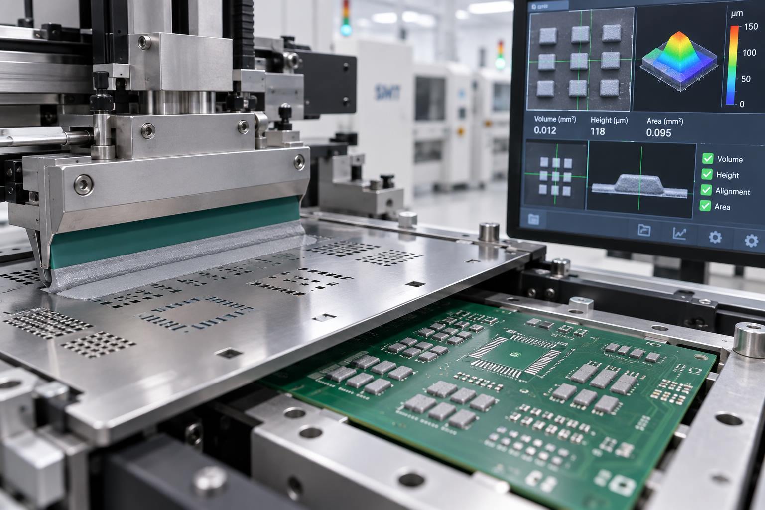
Solder paste printing is controlled by keeping the paste, stencil, printer setup, and board support within a verified operating window.

The main controls work together:

  • Paste condition: Use the specified alloy and flux system, following the supplier’s storage, conditioning, and working-life instructions.
  • Stencil and support: Confirm the stencil revision, aperture condition, underside cleanliness, and support beneath the printed area.
  • Printer settings: Control alignment, squeegee pressure and speed, stencil separation, and the cleaning cycle.

SPI then checks the result on the board, including deposit volume, height, area, and offset. Set the inspection limits for the relevant pad geometry and assembly requirements.

A useful investigation starts with the pattern. As an example, repeated low deposits around one fine-pitch package justify checking those apertures and local board support. A shift across the entire panel calls for an alignment review.

Verify the next prints after an adjustment. For a confirmed failed print, keep the board out of placement until it has an approved disposition, including any required cleaning and reprinting.
PCBA process control

How Is Component Placement Accuracy Controlled in PCBA?

Component placement accuracy is controlled through correct placement data, verified feeder loading, maintained pickup hardware, and checks on the populated board.

The setup has three distinct parts:

  • Program: Coordinates, board side, rotation, package definition, fiducial recognition, and placement height.
  • Material loading: Correct reel or tray, feeder assignment, component orientation, and replenishment checks.
  • Pickup hardware: Suitable nozzles, clean pickup surfaces, reliable vacuum, and correctly indexed feeders.

A first-article check confirms that the setup matches the assembly drawing, especially around polarized devices and fine-pitch packages. Repeat the affected checks after a relevant program, material, or setup change.

Keep positional accuracy separate from component identity. A part can be accurately placed while still being the wrong value or manufacturer part number. Feeder verification addresses that distinction.

During production, review pickup errors and repeated offsets by feeder, nozzle, and component location. In a troubleshooting example, errors associated with one feeder should prompt a local investigation before changing the coordinate origin for the entire board.

How Is the Reflow Soldering Profile Controlled in PCBA?

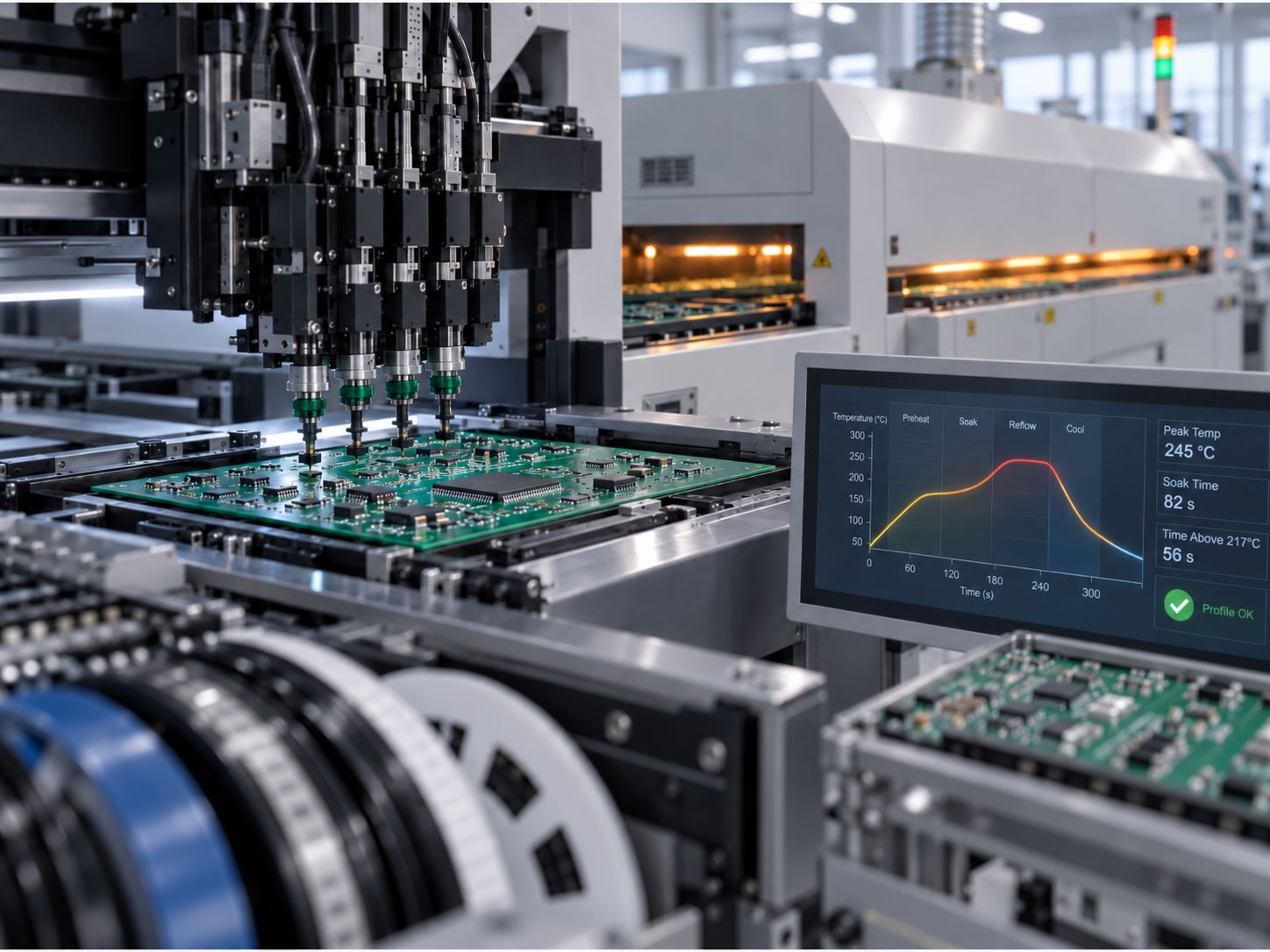
The reflow soldering profile is controlled by measuring temperature over time on a representative assembly and comparing the measurements with the approved thermal window.

That window must accommodate the solder paste, components, and PCB. The main measurements are:

Profile measurement What it establishes
Heating rate How quickly the assembly heats
Soak, when specified Exposure through the selected pre-reflow temperature range
Peak temperature Highest temperature at each monitored location
Time above liquidus Duration above the solder alloy’s liquidus temperature
Cooling rate How quickly the assembly cools after reflow

These measurements should be evaluated together against the selected solder paste’s process requirements.

Attach thermocouples at relevant solder-joint and component locations, including areas expected to heat fastest and slowest. A dense connector area and a small component near the board edge may experience different profiles.

Use the measured results to establish oven zone settings and conveyor speed. Component temperature ratings constrain the profile, while the solder paste has its own process requirements.

Oven setpoints are not the same as temperatures measured on the assembly. Retain the qualified profile with the recipe so repeat builds have a defined thermal reference.
PCBA process control

How Is Through-Hole Soldering Controlled in PCBA?

Through-hole soldering is controlled through flux application, board preheat, solder temperature, contact conditions, and inspection of the completed joints.

The settings depend on the soldering method:

Method Main controls
Wave soldering Flux coverage, preheat, solder temperature, wave height, conveyor speed, and contact time
Selective soldering Flux location, preheat, nozzle condition, solder temperature, travel path, and dwell time
Hand soldering Tip size and condition, verified temperature, solder and flux selection, and contact time

These controls address how flux and heat reach the joint, rather than relying on the solder-pot or iron temperature alone.

Preheat prepares the flux and raises the assembly temperature before solder contact. Areas connected to substantial copper deserve particular attention during thermal verification.

For an insufficient-hole-fill investigation, review heat delivery and flux coverage alongside lead-to-hole fit and solder access. Increasing solder temperature alone may leave the underlying issue unresolved.

Inspect wetting, hole fill, bridging, and other applicable features against the agreed acceptance criteria. Group joints by their demonstrated process needs where appropriate; a large power connector and a small signal header may need different selective-soldering settings.

How Do Inspection and Test Data Support PCBA Process Control?

Inspection and test data support PCBA process control by showing which defects recur, where they occur, and whether an adjustment improves the result.

Organize findings by reference designator, defect type, board identity, and production time. Compare like-for-like builds and consistent test coverage when reviewing trends.

For example, repeated AOI findings at the same component location provide a starting point for checking the placement and soldering process. Confirm the reported condition before changing settings. Electrical failures also warrant a fixture and probe-contact check, since test-system faults can affect results.

Track first-pass yield separately from final yield. First-pass yield counts assemblies that complete the defined operation successfully without repair or retest.

Suppose 100 boards enter a test operation, 96 pass immediately, and four pass after rework. First-pass yield is 96%, while final yield is 100%. Keeping both figures shows the work required to achieve the shipment result.

PCBA process control

How Is SPC Used to Monitor PCBA Process Stability?

Statistical process control (SPC) monitors PCBA process stability by tracking comparable measurements over time and looking for statistically meaningful changes.

Start with a defined characteristic, such as paste volume for one pad type. Confirm measurement repeatability, collect data in production order, and select a control chart suited to the data and sampling method.

The distinction between limits is important:

  • Control limits come from process data and help identify changes in behavior.
  • Specification limits come from engineering or customer requirements and define acceptable output.
  • Capability indices, including Cp and Cpk, compare a stable process with those specification limits.

For example, a paste-volume trend can trigger investigation while individual deposits remain within specification. Follow the chart’s defined signal rules rather than adjusting the printer after every small fluctuation.

Evaluate capability after confirming stability and suitable data assumptions. Standard Cp and Cpk interpretation assumes normally distributed measurements. Group pads with different volume targets separately so their individual process behavior remains visible.

How Are PCBA Process Deviations Handled?

PCBA process deviations are handled by confirming the issue, containing potentially affected assemblies, correcting the cause, and verifying conditions before production resumes.

A practical response follows five steps:

  1. Confirm the finding. Check the board, measurement, equipment status, and applicable program. Determine whether the issue is a product defect, process deviation, or measurement error.
  2. Establish the affected scope. Identify the relevant material lot, production interval, equipment, and boards. Hold potentially affected assemblies while their status is evaluated.
  3. Investigate the cause. Compare the issue with feeder changes, replenishment, maintenance, material substitutions, and process adjustments. Use measurements and controlled trials to test the likely explanation.
  4. Correct and verify. Apply the approved action, repeat the relevant setup or first-article checks, and confirm that subsequent results meet the defined requirements.
  5. Authorize restart and product disposition. Release the process through the designated approver. Separately decide whether held boards can be released, reworked, repaired with authorization, or scrapped.

In a wrong-reel example, the affected scope includes boards populated since that reel was loaded. Replacing the reel fixes the ongoing setup; the already-built boards still require evaluation.

Continue the specified monitoring after restart and update the relevant instruction when the investigation identifies a lasting process change. A successful trial supports restart; the follow-up results show whether the correction remains effective.

What Records Are Needed for PCBA Process Traceability?

PCBA process traceability requires records that connect an assembly’s batch or serial number with its materials, manufacturing history, and quality results.

The record structure should cover:

  • Materials: PCB and component lots, solder paste identity, approved substitutions, and relevant exposure records.
  • Manufacturing: BOM and drawing revisions, equipment and program versions, production timestamps, and applicable process measurements.
  • Quality: Inspection and test results, failure locations, rework, retests, and final release decisions.

Set the traceability detail and retention period before production. IPC-1782 provides a risk-based framework covering manufacturing and supply-chain traceability, with the required scope agreed between customer and supplier.

Record resolution determines how precisely an investigation can identify affected product. Lot-level information supports batch-level tracking; unit-level links can narrow the scope when the underlying material and process records support that detail.

A useful verification exercise works in both directions: select a finished board and retrieve its history, then select a component lot and identify the assemblies that used it. Include reworked boards in the exercise so replacement components remain connected to the final assembly.

FAQs About PCBA Process Control

1. Which IPC Standards Apply to PCBA Process Control?

IPC J-STD-001 covers soldering materials, methods, and process requirements; IPC-A-610 covers assembly acceptance. J-STD-033 supports moisture-sensitive component handling, and IPC-1782 addresses traceability. Agree on the applicable revisions, product class, and customer requirements before the build.

2. How Often Should a PCBA Reflow Profile Be Verified?

Verify it during qualification, at the interval defined in the control plan, and after changes that could affect board temperatures. Relevant triggers include a new thermal recipe, significant oven maintenance, or changes to the assembly’s thermal characteristics.

3. Can SPC Be Used for Low-Volume PCB Assembly?

Yes, when the measurements are comparable and the dataset supports the chosen method. Small batches may need data accumulated across comparable runs. Use setup verification and first-article checks while establishing a baseline, and assess capability only when its statistical prerequisites are met.

4. Does Every PCBA Require X-Ray Inspection?

No. X-ray coverage should reflect hidden-joint risks, package types, and customer requirements. BGA and QFN connections are common candidates. Define the inspected features and acceptance limits as part of the inspection plan.

5. When Do Component Substitutions Require PCBA Process Revalidation?

Revalidation is needed when a substitution changes conditions covered by the approved process, such as package geometry, moisture sensitivity, or temperature limits. Review the change first, then specify the affected placement, soldering, inspection, and test checks.

For a new PCBA build or a repeat order with changes, send your Gerber files, BOM, placement data, assembly drawings, and test requirements to sales@bestpcbs.com. Include the required IPC class and any inspection or traceability deliverables.

EBest Circuit provides PCB fabrication, component sourcing, assembly, and testing. Share critical packages, approved substitutions, and previous manufacturing concerns with the project files so the engineering review can focus on the PCBA process control your assembly needs.

You may also like

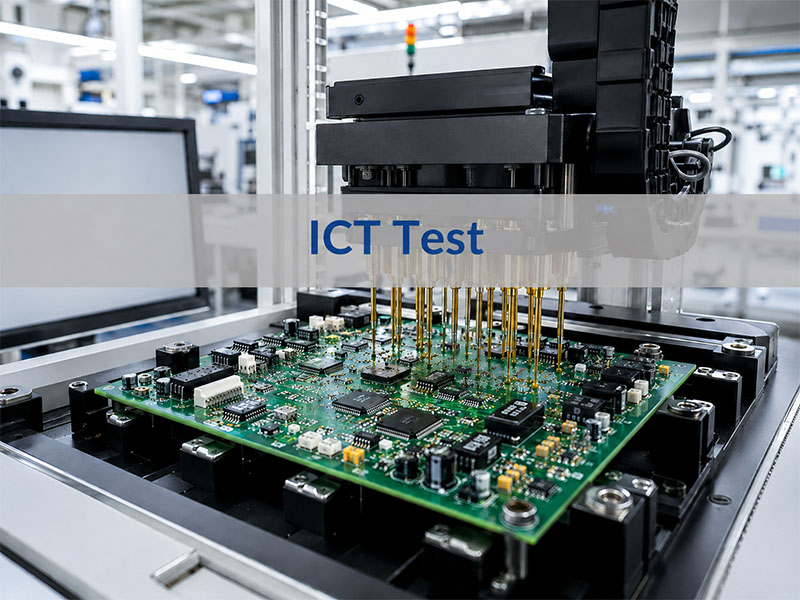
ICT Test: A Practical Guide to In-Circuit Testing for PCB Assembly
Tuesday, May 19th, 2026

An ICT test helps PCB assembly manufacturers check circuit quality before boards move to final inspection or shipment. During PCBA production, small defects can hide under components, inside solder joints, or between fine-pitch pads. Visual inspection may miss them. AOI may also miss some electrical faults. Therefore, in-circuit testing gives engineers a faster and more direct way to check whether the assembled PCB matches the design. In this guide, you will learn what ICT testing means, how the process works, why test points matter, and how ICT compares with FCT and flying probe testing.

ict test

What Is an ICT Test in PCB Assembly?

An ICT test, or In-Circuit Test, checks an assembled PCB at the component and circuit level. Manufacturers usually use it after SMT assembly, DIP soldering, reflow soldering, or wave soldering.

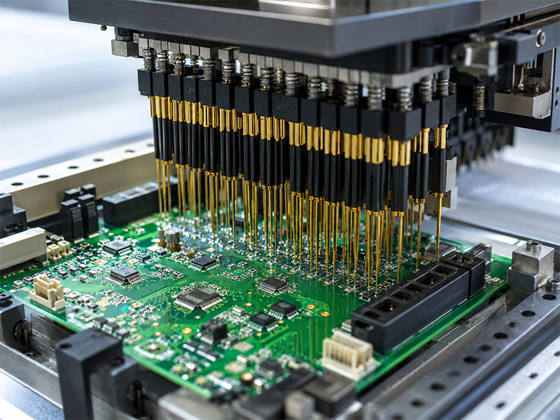
During the test, spring-loaded probes touch selected test points on the PCB. These probes connect the board to an ICT tester. Then, the tester measures electrical values and checks whether the circuit matches the expected design.

In simple words, ICT testing checks whether the PCB assembly was built correctly.

What Does ICT Testing Confirm?

ICT testing can check many basic assembly conditions. For example, it can confirm whether components sit in the right locations. It can also check whether solder joints create a stable electrical connection.

In addition, it helps engineers find:

  • Short circuits
  • Open circuits
  • Wrong component values
  • Missing components
  • Reversed diodes or capacitors
  • Poor solder joints
  • Incorrect IC pin connections
  • Basic power rail problems

As a result, ICT testing gives manufacturers a clear view of board-level assembly quality.

Why Is ICT Important for PCBA Quality?

ICT does more than separate pass and fail boards. It also helps engineers find process trends.

For example, if many boards fail at the same resistor, the issue may come from placement, solder paste, component supply, or PCB pad design. Therefore, the test result can guide process improvement.

This makes ICT useful for both inspection and manufacturing control.

Why Is ICT Test Done During PCBA Manufacturing?

Manufacturers perform ICT testing to find assembly defects early. This is important because early detection saves time, reduces rework, and improves final product quality.

If a board reaches functional testing with many basic faults, engineers may spend more time troubleshooting. However, ICT can detect many of these faults before the final test stage. Therefore, the whole production flow becomes smoother.

ICT Helps Find Defects Earlier

Many PCBA defects start at the assembly stage. Some defects come from solder paste printing. Others come from placement, reflow, component polarity, or PCB design.

ICT can find common defects such as:

  • Solder bridges
  • Open solder joints
  • Wrong resistors
  • Missing capacitors
  • Reversed diodes
  • Lifted IC pins
  • Shorts between power and ground
  • Poor contact on important nets

Because ICT checks the board at the circuit level, it can find problems that visual inspection may not reveal.

ICT Reduces Troubleshooting Time

A functional test may show that a board does not work. However, it may not show the exact reason.

ICT gives more specific information. It can point to a certain net, component, pin, or test point. As a result, engineers can locate the failure faster.

For example, FCT may show that a control board cannot power on. ICT may show that a power rail has a short. This saves time and makes repair work more efficient.

ICT Supports Stable Mass Production

ICT testing works especially well for medium- and high-volume PCBA production. Once engineers complete the fixture and test program, operators can test each board quickly.

This creates a repeatable standard for every production batch. Moreover, the factory can collect failure data and monitor process stability over time.

Therefore, ICT is not only a test method. It also supports long-term quality management.

What Does an ICT Tester Check on a PCB?

An ICT tester checks whether the assembled PCB matches the expected electrical design. The exact coverage depends on the board layout, test points, fixture quality, and test program.

In most cases, the tester checks component values, circuit continuity, short circuits, and basic semiconductor behavior. It may also check some powered circuits, depending on the product and fixture design.

Common ICT Test Items

ICT Test ItemWhat It ChecksTypical Defects Found
Open Circuit TestWhether a circuit path has a proper connectionBroken trace, poor solder joint, missing connection
Short Circuit TestWhether two nets connect by mistakeSolder bridge, copper residue, layout issue
Resistance TestWhether the resistor value matches the designWrong resistor, missing resistor, poor soldering
Capacitance TestWhether the capacitor value stays within rangeWrong capacitor, missing capacitor, polarity issue
Diode TestForward and reverse behaviorReversed diode, wrong diode, poor contact
Transistor TestBasic semiconductor behaviorWrong part, weak soldering, wrong mounting
IC Pin TestPin connection and basic responseLifted pin, solder bridge, poor wetting
Polarity CheckOrientation of polarized componentsReversed diode, reversed capacitor
Power Net CheckPower rail conditionShort on power line, unstable connection

What ICT Cannot Fully Check

ICT is powerful, but it does not replace every other test. For example, it may not fully check firmware, wireless communication, display behavior, motor control, or sensor response.

Therefore, many manufacturers combine ICT with FCT. ICT checks the circuit build quality. Then, FCT checks whether the board works in its real application.

This combined method gives better quality coverage.

How Does the ICT Test Procedure Work?

The ICT test procedure starts before production testing. Engineers need to review files, define test points, design the fixture, build the test program, and debug the setup.

A clear process helps improve test coverage and reduce false failures. Moreover, it helps the factory prepare for stable production.

Step 1: Review PCB Design Files

First, engineers review the Gerber files, BOM, schematic, netlist, assembly drawing, and test requirements.

This review helps them understand the circuit structure. It also helps them decide which nets and components need testing.

At this stage, engineers may also find layout issues that affect test access.

Step 2: Define ICT Test Points

Next, engineers check the test point layout. Each important net should have a clear and reachable test point.

Good test points help the fixture contact the PCB with stable pressure. In contrast, poor test points may reduce coverage and create false failures.

Therefore, test point review should happen before mass production.

Step 3: Design the ICT Fixture

After that, the fixture team designs the ICT test fixture. The design depends on board size, panel layout, test point locations, component height, and board thickness.

The fixture must hold the PCB firmly. It must also align the probes with the test points accurately.

Good fixture design improves test stability and reduces repeat test issues.

Step 4: Develop the Test Program

The test program tells the ICT tester what to measure. It also defines the acceptable range for each test item.

For example, the program may include resistance limits, capacitance tolerance, diode voltage range, and short/open limits.

A well-built program helps the tester judge each board consistently.

Step 5: Debug and Verify the Setup

Before mass production, engineers debug the fixture and program with sample boards.

During this stage, they check probe contact, adjust limits, and remove false failures. They also compare ICT results with actual board conditions.

Once the setup becomes stable, the production team can start routine testing.

Step 6: Run Production Testing

During production, operators place each PCBA into the fixture and start the test. The tester then gives a pass or fail result.

If the board fails, the team separates it for repair or engineering review. Meanwhile, pass boards move to the next process.

This keeps the production flow organized.

Step 7: Analyze Failure Data

Finally, engineers review ICT failure data. If the same fault appears many times, they investigate the root cause.

The issue may come from stencil design, solder paste volume, placement accuracy, reflow profile, component quality, or PCB layout.

Therefore, ICT data can help improve the whole assembly process.

What Are ICT Test Points and Why Do They Matter?

ICT test points are exposed copper pads or contact areas on a PCB. Test probes touch these points during in-circuit testing.

Without good test points, even a strong ICT tester cannot deliver high coverage. Therefore, test point design plays a major role in PCBA testability.

Why Test Points Affect Coverage

Every important circuit net needs access. If a net has no test point, the ICT fixture may not check it directly.

As a result, test coverage drops. Also, the test may miss certain open circuits or weak connections.

Good test points help the fixture contact the board reliably. They also reduce false failures caused by poor probe contact.

Key ICT Test Point Design Tips

Design FactorPractical Recommendation
Test Point SizeMake the pad large enough for stable probe contact
SpacingKeep enough clearance between nearby test points
Solder Mask OpeningExpose a clean copper area for the probe
LocationAvoid tall parts, board edges, and blocked zones
DistributionSpread points evenly when possible
Surface FinishChoose a finish that supports stable contact
AccessibilityPrefer one-side access when the layout allows it
Mechanical SupportAdd support pins when probe force may bend the board

When Should Engineers Plan Test Points?

Engineers should plan ICT test points during PCB layout. This timing matters.

If the team thinks about ICT after the design is complete, changes may become harder. The customer may need to revise the layout, delay production, or accept lower test coverage.

Therefore, DFM review should include testability review. This is especially important for products that will enter repeat production.

What Is an ICT Test Fixture?

An ICT test fixture connects the assembled PCB to the ICT tester. Many people also call it a “bed-of-nails” fixture because it uses many spring-loaded probes.

The fixture positions the board, aligns the probes, and creates electrical contact with the test points. Without a reliable fixture, ICT results may become unstable.

Main Parts of an ICT Fixture

A typical ICT fixture may include:

  • Probe plate
  • Spring-loaded pogo pins
  • Alignment pins
  • Board support pins
  • Press structure or vacuum structure
  • Interface wiring
  • Connector interface
  • Board positioning frame
  • Safety cover

Each part helps the fixture contact the PCB accurately and safely.

Why Custom Fixture Design Matters

Manufacturers design each ICT fixture for a specific PCB or panel. Therefore, fixture design must match the actual product.

Several factors affect the fixture:

FactorWhy It Matters
PCB SizeIt affects fixture structure and board support
Panel DesignIt affects probe layout and handling efficiency
Test Point CountMore points require more probes and wiring
Component HeightTall parts need enough fixture clearance
Board ThicknessThin boards may need extra support
Probe SideSingle-sided probing is simpler than double-sided probing
Production VolumeHigh-volume products need durable fixtures

How a Good Fixture Improves Testing

A good fixture improves contact stability. It also reduces false failures and repeat testing.

For example, if the fixture does not support the board well, probe pressure may bend the PCB. Then, some probes may lose contact. This can create false failures.

Therefore, fixture debugging is a key step before mass production.

ICT Test vs FCT Test: What Is the Difference?

ICT and FCT both support PCBA quality control. However, they check different things.

ICT checks how the board was assembled. FCT checks how the board works.

Because of this difference, many manufacturers use both methods in one test strategy.

ICT vs FCT Comparison

ItemICT TestFCT Test
Full NameIn-Circuit TestFunctional Circuit Test
Main PurposeCheck assembly quality and circuit connectivityCheck final product function
Test LevelComponent and net levelSystem or application level
Test MethodProbes contact PCB test pointsBoard runs in a simulated working condition
Fixture TypeBed-of-nails fixtureFunctional test jig
Common Defects FoundOpens, shorts, wrong values, missing parts, reversed partsFirmware issues, communication failure, power-up problems, signal errors
Test SpeedFast after setupDepends on product function
Best Use CaseMedium- and high-volume PCBA productionProduct-level verification
Main LimitationIt does not fully check real-world operationIt may not locate component-level faults quickly

When Should You Use ICT and FCT Together?

For many products, the best answer is not ICT or FCT. Instead, the better option is ICT plus FCT.

First, ICT checks whether the circuit was assembled correctly. Then, FCT checks whether the product performs its intended function.

This approach works well for industrial control boards, medical electronics, communication modules, automotive electronics, LED control boards, and power control products.

As a result, the manufacturer can catch both assembly-level faults and function-level issues.

Flying Probe Test vs ICT Test: Which One Should You Choose?

Flying probe testing and ICT testing both check electrical conditions on a PCB assembly. However, they suit different production stages.

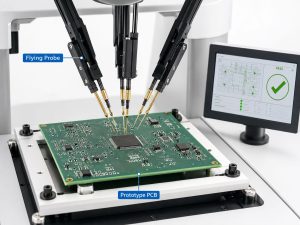
A flying probe test uses moving probes. It does not need a dedicated bed-of-nails fixture. Therefore, it works well for prototypes and small batches.

ICT uses a custom fixture. Because of that, it offers faster testing for stable and higher-volume production.

Flying Probe vs ICT Comparison

ItemFlying Probe TestICT Test
Fixture RequirementNo dedicated fixtureCustom fixture required
Setup CostLowerHigher initial fixture cost
Test SpeedSlowerFaster
FlexibilityHighLower after fixture completion
Best ForPrototype and small-batch productionMedium- and high-volume production
Design ChangesEasy to adaptFixture may need modification
Unit Cost in VolumeHigherLower after fixture cost spreads across volume
Test CoverageGood for accessible netsStrong when test points are well designed

When Flying Probe Makes More Sense

Flying probe testing is a good choice for prototypes. It also works well when the PCB design may still change.

At this stage, the customer may only need a few boards. In that case, building a custom ICT fixture may not make sense.

In addition, flying probe testing gives engineers more flexibility during early product development.

When ICT Makes More Sense

ICT becomes more attractive when the design becomes stable. It also works better when the order quantity increases.

Although the fixture has an initial cost, the test speed is much faster. Over many boards, the cost per unit becomes more reasonable.

Therefore, ICT often fits repeat orders, stable PCB assemblies, and mass production.

Simple Selection Guide

Project SituationBetter Choice
Prototype onlyFlying probe
Small batch with frequent design changesFlying probe
Stable design with repeat ordersICT
Medium-volume productionICT
High-volume productionICT
Need fast fault location in productionICT
No proper test pointsFlying probe may be more practical

In practice, the best test method depends on product complexity, order volume, layout condition, and reliability needs.

FAQs About ICT Test

1. Can ICT testing find every PCBA defect?

No. ICT testing can find many circuit-level and component-level defects. However, it cannot check every real operating function.

For better coverage, manufacturers often combine ICT with FCT, AOI, X-ray inspection, and visual inspection.

2. Is an ICT fixture worth the cost for small batches?

Usually, an ICT fixture fits stable and repeat production better. For prototypes or small batches, flying probe testing may offer better value.

However, if the product will move into mass production soon, early ICT planning can still help.

3. What affects ICT test coverage?

ICT test coverage depends on test point access, PCB layout, component type, fixture design, probe contact, and test program quality.

Therefore, engineers should review testability during the DFM stage.

4. Why do some boards fail ICT even when they look correct?

Some defects are not easy to see. For example, a solder joint may look good but still have weak electrical contact.

Also, a component may sit in the correct location but have the wrong value. ICT helps detect these hidden issues.

5. Can ICT testing replace functional testing?

No, in most cases. ICT checks circuit assembly quality. FCT checks whether the board works in its final application.

Therefore, both methods often work together in a complete PCBA test plan.

6. When should ICT test points be designed?

Engineers should design ICT test points during PCB layout. This gives the layout team more freedom to place clear and stable test pads.

If the team waits until production, changes may cost more time.

7. What is the difference between ICT test pins and ICT test probes?

In daily production, people often use these two terms in a similar way. They usually refer to the spring-loaded contact parts inside the test fixture.

These probes touch the PCB test points during testing.

8. How does ICT testing help PCBA manufacturers improve quality?

ICT testing gives fast and detailed failure data. Engineers can use this data to find repeated issues and improve the process.

For example, they may adjust stencil design, placement settings, reflow profile, or test point layout.

9. Should every PCB assembly project use ICT testing?

Not every project needs ICT. The right choice depends on product complexity, order quantity, budget, and reliability needs.

For stable medium- or high-volume PCB assemblies, ICT is often a strong and practical choice.

You may also like