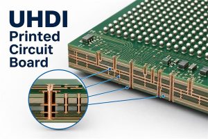
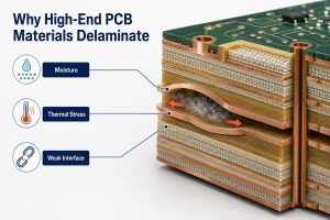
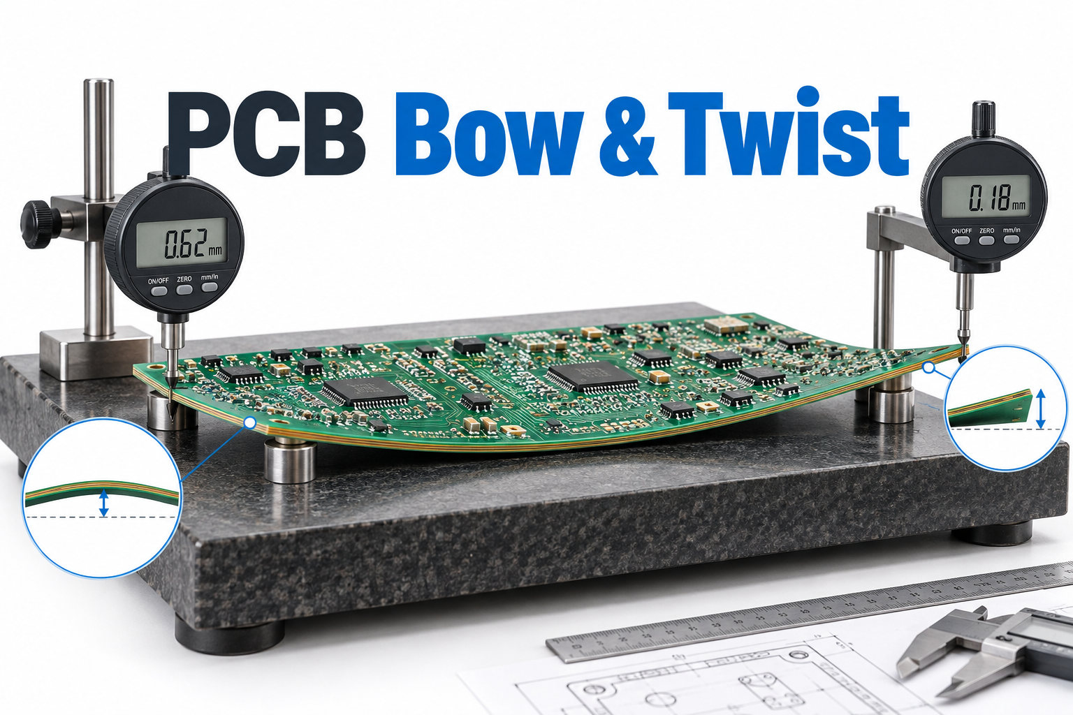
PCB bow and twist are forms of PCB warpage that can affect solder paste printing, component coplanarity, connector fit, automated handling, and final mechanical assembly. The percentage may look small, but on a large or thin PCB, even a fraction of one percent can produce several millimeters of displacement.
For engineers and buyers, the practical questions are therefore not only “Is the board warped?” but how the deformation is classified, how it is measured, which IPC requirement applies, and whether the board meets the agreed flatness specification.
Key Takeaways
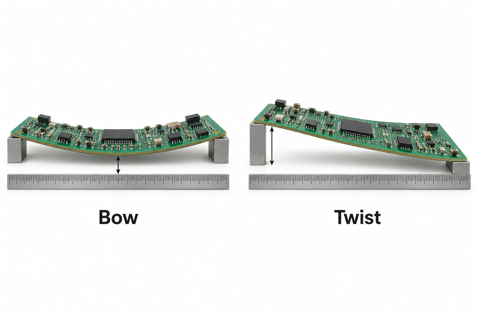
- PCB bow is a curved deformation, while PCB twist is a diagonal deformation that lifts one corner out of the plane formed by the other three corners.
- IPC-6012F specifies a default maximum bow and twist of 0.75% for printed boards using surface-mount components and 1.5% for other printed boards, unless procurement documentation specifies otherwise.
- IPC-TM-650 2.4.22 is the key test method for determining bow and twist percentage on rigid printed boards, rigid portions of rigid-flex boards, and multiple-board panels.
- For bow, the measured gap is divided by the corresponding board length or width. For production-method twist, the lifted-corner gap is divided by twice the board diagonal.
- A 200 × 300 mm SMT PCB with a 0.75% limit allows 1.50 mm bow across the 200 mm direction, 2.25 mm across the 300 mm direction, and approximately 5.41 mm raised-corner gap for the IPC production twist method.
- Asymmetric stackups, uneven copper distribution, material construction, lamination conditions, and later thermal or mechanical stress can all contribute to PCB warpage.
- The IPC 0.75% value is an acceptance limit, not necessarily the optimum flatness target for every assembly.
What Are PCB Bow and Twist?
PCB bow and twist are two different forms of deviation from flatness. PCB bow is roughly cylindrical or spherical curvature in which the four corners of a rectangular board remain in one plane, while twist occurs along a diagonal so that one corner lies outside the plane formed by the other three.
| Characteristic | PCB Bow | PCB Twist |
|---|---|---|
| Typical shape | Arc, hump, or shallow dome | Propeller-like diagonal distortion |
| Corner condition | Four corners can remain coplanar | One corner lifts relative to the other three |
| Main measurement reference | Board length and width | Board diagonal |
| Production measurement | Maximum gap along an edge direction | Raised-corner gap |
A board can also show a combination of bow and twist. In that case, simply measuring the highest point from a tabletop does not necessarily produce the correct IPC percentage.
The test setup and calculation method need to match the type of deformation being evaluated.
What Is the IPC Standard for PCB Bow and Twist?
IPC-6012F specifies that, unless otherwise stated in the procurement documentation, finished rigid printed boards designed in accordance with IPC-2221 have a maximum bow and twist of 0.75% when surface-mount components are used and 1.5% for other printed boards.
| Board Application | Default IPC-6012F Maximum |
|---|---|
| Printed board using surface-mount components | 0.75% |
| Other printed boards | 1.50% |
These percentages are default acceptance requirements, not universal design targets. A customer drawing, procurement specification, or product-specific requirement can call for tighter flatness.
Finished boards are also assessed in their delivered form. If boards are supplied in pallet arrays for assembly, the bow and twist requirement for the array may be agreed separately between the user and supplier.
IPC-TM-650 2.4.22 vs 2.4.22.1: What Is the Difference?
IPC-TM-650 2.4.22 and 2.4.22.1 sound nearly identical, but they report flatness differently.
| Test Method | Main Purpose | Result |
|---|---|---|
| IPC-TM-650 2.4.22C | Bow and twist of rigid boards, rigid portions of rigid-flex, and multiple-board panels | Percentage |
| IPC-TM-650 2.4.22.1C | Maximum vertical displacement of panels, finished rigid boards, and rigid portions of rigid-flex | Displacement in mm/in |
Method 2.4.22 includes production Go/No-Go procedures for bow and twist, plus a more precise referee procedure for twist. It uses a precision surface plate, feeler or pin gauges, measuring devices, and, for the referee method, additional support and dial-indicator equipment.
Method 2.4.22.1 instead records the maximum vertical displacement of an unrestrained specimen. Its scope applies to laminates at least 0.5 mm [0.020 in] thick and can also be used after etching or thermal stress when agreed between user and supplier.
These methods should therefore not be treated as interchangeable calculations.
How Do You Measure PCB Bow?
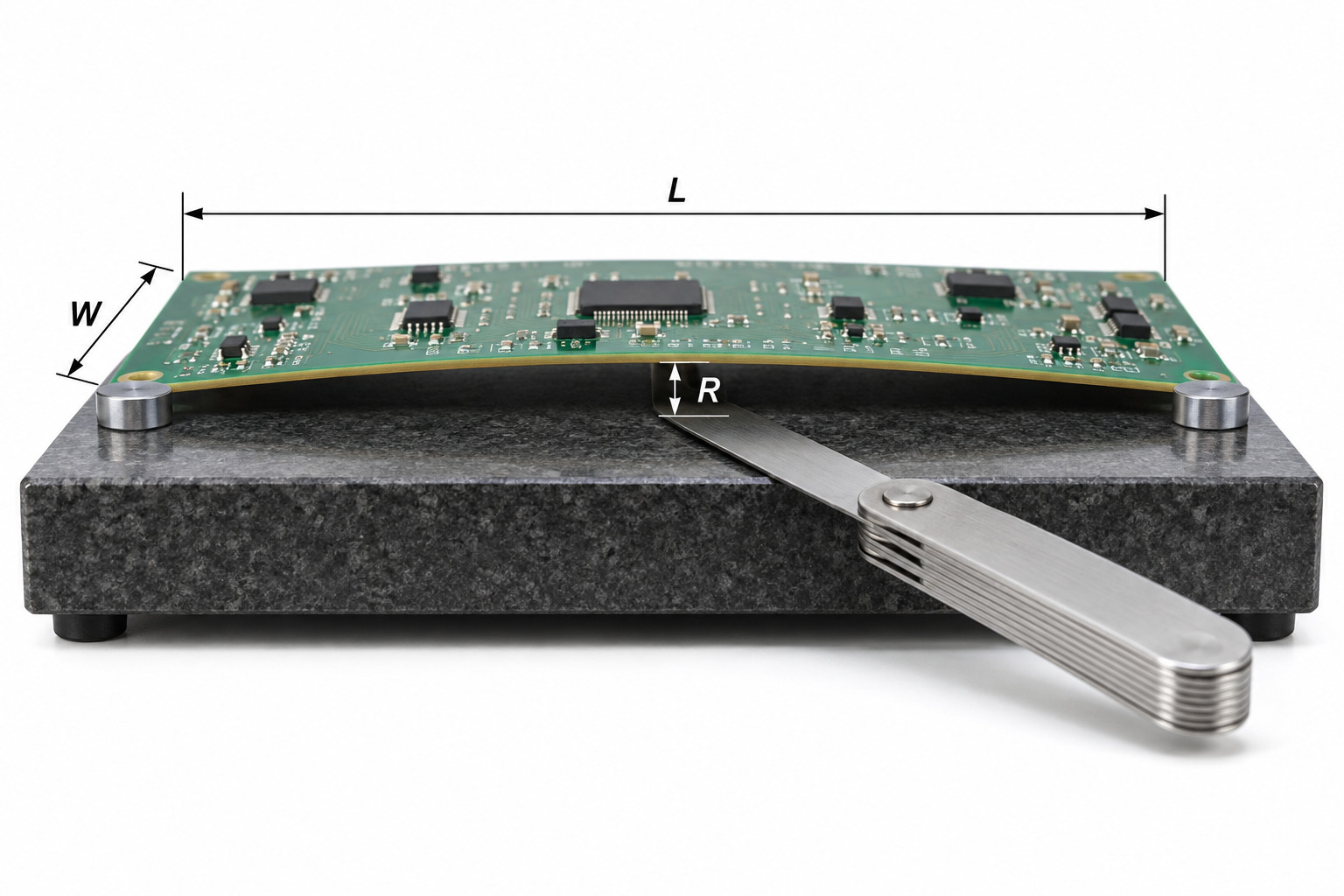
PCB bow is measured by placing the board on a precision flat surface with the convex side facing upward and measuring the gap created by the curvature. A bow and twist PCB check should classify the deformation before selecting the measurement method.
For the IPC-TM-650 2.4.22 production method:
- Measure the board length L and width W.
- Place the board on a precision surface plate, convex side upward.
- For the edge being checked, apply enough pressure at both corners of that edge to bring them into contact with the datum surface.
- Insert a feeler or pin gauge between the PCB and surface plate.
- Determine the largest gauge that fits for the length and width directions.
- Record these measurements as RL and RW.
- Calculate bow percentage separately for length and width.
IPC calculates bow in the corresponding board direction. The denominator is not automatically the PCB diagonal.
This distinction matters because using the diagonal would produce a lower calculated percentage and could incorrectly classify an out-of-tolerance board as acceptable.
How Do You Measure PCB Twist?
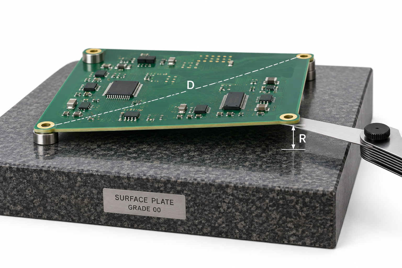
For production testing, PCB twist is measured by placing three corners of the board against a flat datum surface and measuring the gap beneath the remaining lifted corner.
The IPC-TM-650 2.4.22 procedure is:
- Measure the board diagonal and record it as D.
- Place the PCB on the surface plate.
- Position it so that three corners contact the surface.
- If necessary, restrain only one corner to establish three-point contact.
- Insert a feeler or pin gauge under the remaining lifted corner.
- Find the largest gauge that fits without lifting the other three corners.
- Record that gap as R.
- Calculate the twist percentage.
The production formula contains a factor of two because constraining one corner against the surface plate approximately doubles the observed vertical twist deflection.
If three corners cannot be brought into contact by restraining only one corner, the referee method should be used instead of forcing the production procedure.
What Is the PCB Bow and Twist Formula?
IPC-TM-650 2.4.22 uses different formulas for bow and production-method twist. A PCB bow and twist calculator must use the correct board direction or diagonal for the deformation being measured.
Bow in the length direction:
BowL (%) = (RL / L) × 100
Bow in the width direction:
BowW (%) = (RW / W) × 100
Where:
- RL = maximum measured gap in the length direction
- RW = maximum measured gap in the width direction
- L = PCB length
- W = PCB width
Twist — production method:
Twist (%) = (R / (2 × D)) × 100
Where:
- R = maximum gap under the raised corner
- D = PCB diagonal
The factor of two should not be removed when using this IPC production measurement method.
For a rectangular PCB, the diagonal is:
D = √(L² + W²)
How Do You Calculate PCB Bow and Twist?
Consider a 200 × 300 mm PCB that will use SMT components. Using the default IPC-6012F limit of 0.75%, the maximum allowable production-measurement gaps can be calculated before inspection.
The PCB bow and twist percentage must always be evaluated against the board dimensions and the agreed acceptance limit.
PCB dimensions
- Width = 200 mm
- Length = 300 mm
- Bow/twist limit = 0.75%
First calculate the board diagonal:
D = √(200² + 300²) = 360.56 mm
The allowable gaps are:
| Calculation | Formula | Maximum Gap |
|---|---|---|
| Bow across 200 mm direction | 200 × 0.75% | 1.50 mm |
| Bow across 300 mm direction | 300 × 0.75% | 2.25 mm |
| Twist production gap | 2 × 360.56 × 0.75% | 5.41 mm |
Now assume the measured 300 mm-direction bow gap is 1.80 mm:
Bow = (1.80 / 300) × 100 = 0.60%
That result is below 0.75%.
If the measured lifted-corner gap for twist is 4.00 mm:
Twist = (4.00 / (2 × 360.56)) × 100 ≈ 0.55%
That result is also below 0.75%.
This example shows why a physical gap in millimeters cannot be judged by itself. The same displacement produces a different bow or twist percentage depending on board dimensions.
What Causes PCB Bow and Twist?
PCB bow and twist usually result from uneven internal stress rather than one isolated defect. The source can enter during design, material preparation, fabrication, or later thermal processing.
Evaluating bow and twist in PCB production starts with identifying where uneven stress entered the process.
PCB Design
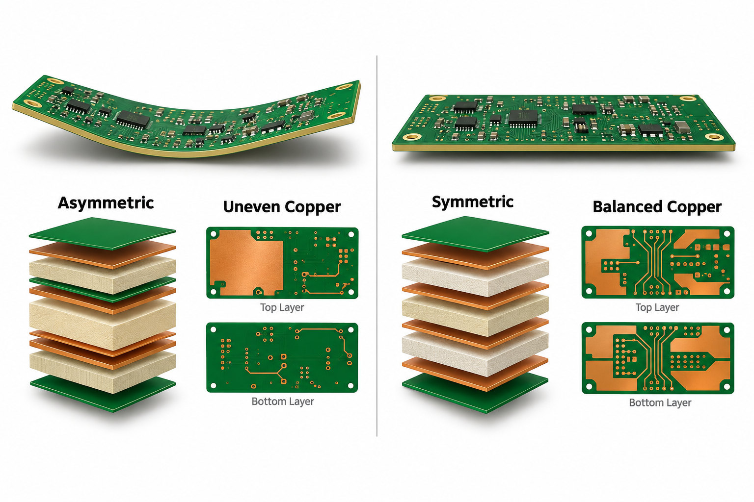
Common design-related contributors include asymmetric stackups, unequal copper weights above and below the centerline, large differences in local copper density, large cutouts, and panel breakaway areas that do not reflect the copper distribution of the finished board.
Materials
Glass-fabric orientation, core and prepreg construction, CTE mismatch, mixed laminate systems, and moisture condition can affect dimensional stability.
Press conditions, incomplete cure, incorrect prepreg construction, uneven heating or cooling, solder-mask cure, and hot-air solder leveling can introduce or release stress.
Assembly and Handling
Mechanical loading, storage, reflow, fixtures, conveyor support, and asymmetric component mass can further change the board shape.
A useful way to think about these mechanisms is that some stress is built into the PCB during lamination, while other deformation is introduced later by handling or thermal processing.
Why Does Copper Distribution Affect PCB Warpage?
Copper and dielectric materials respond differently to temperature and processing stress, so an unbalanced copper pattern can create unequal forces through the PCB thickness.
The problem can occur in two ways:
- Layer-to-layer imbalance: one side of the stack has heavier copper or larger plane areas than its mirrored layer.
- Local imbalance: one region contains dense copper while another region contains very little copper.
During multilayer pressing, copper density also affects resin flow and local pressure. During later thermal cycles, different copper distributions can contribute to unequal expansion and stress.
A symmetrical stackup with similar copper weights and coverage on corresponding layers reduces this risk. Panel breakaway areas should also avoid extreme copper-density differences compared with the PCB itself.
Copper filling or thieving may help balance sparse areas, but it should still respect electrical clearance, impedance, creepage, and signal-integrity requirements.
How Can PCB Bow and Twist Be Reduced Before Fabrication?
The most effective time to control PCB warpage is before the stackup and panel design are frozen.
Useful DFM checks include:
- Keep the multilayer stackup symmetric around the centerline.
- Use matching copper weights on mirrored layers where practical.
- Balance copper coverage across opposing sides.
- Review large copper-free or low-density regions.
- Keep core and prepreg construction mechanically balanced.
- Review glass orientation where material construction makes it relevant.
- Consider board thickness relative to size and mechanical support.
- Balance copper in panel rails and breakaway areas.
- Review mixed-material stackups for CTE and lamination compatibility.
- Define any tighter flatness requirement on the drawing before production.
For EBest Circuit projects, bow-and-twist risk can be reviewed during DFM together with stackup construction, copper distribution, panelization, material selection, and finished thickness.
How Is Bow and Twist Controlled During PCB Manufacturing?
Manufacturing control focuses on preventing uneven stress from being built into or released from the panel.
Important process controls include:
- Laminate and prepreg storage
- Glass direction and ply construction
- Controlled lamination temperature and pressure
- Resin-flow and cure control
- Symmetrical panel construction
- Copper plating balance
- Solder-mask and legend curing
- HASL or other high-temperature processing
- Panel support during handling
- Controlled cooling
- Final flatness inspection
Lamination is particularly important because once intrinsic deformation is locked into the multilayer structure, later flattening may not provide a permanent correction.
Final inspection should be performed on the board in the required delivered form and against the applicable customer or IPC limit.
When Should a PCB Use a Tighter Flatness Limit Than IPC 0.75%?
A tighter requirement may be appropriate whenever the standard 0.75% bare-board limit does not provide enough mechanical or assembly margin.
Examples include boards with:
- Large BGA or fine-pitch area-array packages
- Long board-edge connectors
- Press-fit connector fields
- Tight card-guide or chassis interfaces
- Thin, large-format PCBs
- High-density SMT on both sides
- Precision optical or sensor assemblies
- Customer-defined coplanarity requirements
The correct tighter value depends on the product. It should not be assumed that every BGA board requires 0.5%, 0.3%, or another generic number.
IPC-6012F allows procurement documentation to specify requirements other than the default 0.75% or 1.5% limits.
For tight-flatness projects, the designer and PCB manufacturer should agree on the measurement method, delivery form, panel condition, temperature condition, and acceptance limit before fabrication.
Does IPC-TM-650 Bow and Twist Apply to an Assembled PCBA?
IPC-TM-650 2.4.22 is primarily a bare printed-board flatness test. Its scope covers individual rigid boards, rigid portions of rigid-flex boards, and multiple-board panels, but it does not address all special conditions of populated assemblies such as component weight, placement, edge supports, and connectors.
An assembled PCBA can behave differently because reflow temperature, component packages, heat sinks, connectors, fixtures, and solder joints all influence deformation.
For temperature-dependent board flatness, separate methods may be used to evaluate local board shape through a simulated reflow cycle. These do not replace room-temperature bow and twist inspection of the bare PCB.
Bare-board bow/twist and assembled-PCBA warpage should therefore be treated as related but different engineering problems.
FAQ About PCB Bow and Twist
1. What is the maximum PCB bow and twist allowed by IPC?
IPC-6012F specifies a default maximum of 0.75% for printed boards using surface-mount components and 1.5% for other printed boards, unless procurement documentation requires a different limit.
2. How is PCB bow percentage calculated?
PCB bow percentage is calculated from the maximum measured gap relative to the corresponding board length or width.
3. How is PCB twist percentage calculated?
PCB twist percentage is calculated from the raised-corner gap and the PCB diagonal using the IPC-TM-650 production method.
4. Is PCB bow the same as PCB twist?
No. Bow is a curved deformation in which the four corners can remain coplanar, while twist is a diagonal deformation that raises one corner relative to the other three.
5. What commonly causes excessive PCB warpage?
Asymmetric stackups, uneven copper distribution, material construction, lamination stress, incomplete cure, mechanical handling, and later thermal processes can all contribute.
6. Can a customer specify a tighter bow and twist limit?
Yes. A customer can define a tighter requirement in the procurement documentation, and that agreed requirement takes precedence over the general IPC default for the project.
PCB bow and twist should be controlled from stackup design through final inspection rather than treated only as an end-of-line flatness problem. Symmetry, copper balance, material construction, lamination, panel design, and thermal processing all influence the final result.
For PCB projects with tight flatness requirements, EBest Circuit can review the Gerber files, stackup, copper distribution, panelization, finished thickness, assembly requirements, and target bow/twist limit before production. Send the project data to sales@bestpcbs.com for DFM review.