PCB manufacturing PCB manufacturing
Home > Blog

InP Substrate Guide: Types, Applications, Suppliers, Prices, and Supply Risks

September 7th, 2026

Indium phosphide is a key semiconductor material for optical communication, high-speed photonics, infrared detection, and selected RF devices. Demand has also grown with AI data-center infrastructure, where high-speed optical links increasingly rely on InP-based lasers, detectors, and photonic components.

For engineers and buyers, however, choosing an InP substrate is not simply a matter of ordering a 2-inch or 4-inch wafer. Conductivity type, dopant, crystal quality, EPD, orientation, surface condition, and supplier consistency can all affect epitaxial growth and device yield. This guide explains the main types, applications, available sizes, material alternatives, pricing factors, suppliers, and current supply risks.

InP substrate wafers in a semiconductor photonics laboratory

What Is an Indium Phosphide (InP) Substrate?

An InP substrate is a single-crystal wafer made from indium phosphide, a III-V compound semiconductor consisting of indium and phosphorus.

It is mainly used as the crystalline foundation on which additional semiconductor layers are grown. Materials such as InGaAs, InGaAsP, and InAlAs can be deposited on InP to form active device structures for lasers, photodetectors, modulators, HBTs, HEMTs, and photonic integrated circuits.

The terms InP wafer and InP substrate are often used interchangeably, but the manufacturing context matters:

  • Bare InP substrate: A polished single-crystal wafer before epitaxial growth.
  • Epi-ready InP substrate: A polished and cleaned wafer prepared for MOCVD or MBE epitaxy.
  • InP epiwafer: An InP substrate with one or more epitaxial semiconductor layers already grown on it.

This distinction matters in sourcing. A company that grows bulk InP crystals and supplies polished substrates is providing a different product from an epitaxy supplier offering a completed device layer structure.

What Is an InP Substrate Used For?

InP substrates are mainly used where the device requires long-wavelength photonics, high-speed optical conversion, infrared detection, or very high-frequency electronic performance.

InP substrate applications including optical transceivers, laser diodes, photodetectors, photonic ICs, and RF devices

Typical applications include:

  • Optical transceivers for telecom networks and data centers
  • DFB and FP laser diodes
  • Electro-absorption modulated lasers
  • PIN photodiodes and avalanche photodiodes
  • Photonic integrated circuits
  • Optical modulators and amplifiers
  • Short-wave infrared detectors
  • LiDAR and optical sensing
  • HBT and HEMT devices
  • Millimeter-wave electronics

One of InP’s strongest application areas is optical communication around 1310 nm and 1550 nm. The substrate supports III-V epitaxial systems such as InGaAsP and InAlGaAs that can be engineered for these telecom wavelength bands.

This makes InP particularly useful in laser sources, detectors, and integrated photonic devices used in high-speed optical links. Silicon photonics may handle routing and passive functions in the same module, but active light generation and detection often still rely on III-V materials.

What Types of InP Substrates Are Available?

InP substrates are usually classified by conductivity type and dopant.

Undoped, n-type, p-type, and semi-insulating InP substrate types
InP Substrate Type Common Dopant Electrical Behavior Typical Use
Undoped InP None Usually lightly conductive Epitaxy, research, special structures
n-Type InP S or Sn Electron-conducting Lasers, detectors, optoelectronics
p-Type InP Zn Hole-conducting Selected device structures
Semi-insulating InP Fe Very high resistivity RF, HBT, HEMT and isolated device structures

Semi-insulating InP substrate is especially important for high-frequency electronics. Its high resistivity helps limit unwanted current paths through the substrate and improves isolation between active areas.

Specifying only “n-type” or “semi-insulating” is not enough for production purchasing. The RFQ should also define the required:

  • Carrier concentration
  • Resistivity
  • Mobility, where relevant
  • Dopant type
  • Electrical tolerance range

Two wafers sold under the same general category can still have substantially different electrical characteristics.

What Sizes Are InP Substrates Available In?

Commercial InP substrates are commonly available in 2-inch, 3-inch, and 4-inch diameters, while 6-inch InP is becoming more important for higher-volume manufacturing.

Comparison of 2-inch, 3-inch, 4-inch, and 6-inch InP substrate wafer sizes
Nominal Size Diameter Typical Use
2 inch 50.8 mm R&D, legacy production, specialty devices
3 inch 76.2 mm Established compound-semiconductor production
4 inch 100 mm Common modern production platform
6 inch 150 mm Higher-volume and newer manufacturing platforms

Availability varies by supplier. A manufacturer that routinely ships 3- or 4-inch material may not have qualified 6-inch capacity.

Larger wafers can improve production economics because more dies are processed in one batch, but scaling InP crystal growth is difficult. Maintaining low EPD, good flatness, uniform electrical properties, and acceptable yield becomes harder as crystal diameter increases.

For that reason, a 6-inch requirement should be discussed with suppliers early. Do not assume it will have the same lead time, grade availability, or supplier base as 4-inch material.

InP vs GaAs vs Silicon: When Should You Use Each Substrate?

InP is not the best substrate for every semiconductor device. It becomes attractive when its material system provides a performance advantage that is difficult to reproduce with GaAs or silicon.

Selection Factor InP GaAs Silicon
1310/1550 nm photonics Excellent Limited Strong passive platform
Native light generation Excellent Excellent in suitable wavelengths Poor
High-frequency electronics Excellent Excellent Good
Photonic integration Strong Application-dependent Very strong ecosystem
Large wafer availability Limited Better than InP Excellent
Material cost High High Low
Manufacturing scale Specialized Mature III-V Extremely mature

Use InP when the device architecture depends on:

  • InGaAs-based photodetection
  • Long-wavelength semiconductor lasers
  • High-speed InP HBTs
  • Integrated III-V photonics
  • Epitaxial structures lattice-matched to InP

GaAs is often more suitable for VCSELs, RF amplifiers, LEDs, and some sensing systems. Silicon remains the preferred choice when low cost, large wafer size, CMOS compatibility, and mature manufacturing are more important than native III-V optical performance.

The material choice should therefore start with device physics rather than wafer price.

How Much Does an InP Substrate Cost?

InP substrate prices vary widely, so there is no reliable single market price.

InP substrate supply and price drivers including wafer diameter, dopant, EPD, supplier capacity, and AI optical demand

Small research-grade wafers may cost hundreds of dollars, while larger production-grade, low-defect, or epi-ready wafers can reach four-figure prices per wafer. During supply shortages, pricing can rise well beyond normal levels.

An InP substrate price quote should therefore be compared against the complete wafer specification and supply terms. The main price drivers include:

  • Wafer diameter
  • Conductivity type
  • Dopant
  • EPD requirement
  • Crystal quality
  • SSP or DSP polishing
  • Epi-ready finishing
  • Orientation tolerance
  • Flatness requirements
  • Inspection level
  • Quantity
  • Supplier capacity

A quotation issued during a shortage may also reflect capacity allocation rather than normal manufacturing cost.

When comparing InP substrate suppliers, send the same specification to each company. Otherwise, a lower price may simply correspond to a higher EPD, wider geometric tolerance, different polishing grade, or less demanding inspection criteria.

Why Are InP Substrates in Short Supply?

The current shortage is largely the result of fast-growing optical demand meeting a relatively concentrated substrate manufacturing base.

Several factors are involved:

  • AI data-center growth: Faster optical interconnects require more lasers, detectors, and optical transceiver components.
  • Limited crystal-growth capacity: High-quality InP single-crystal production is difficult to scale quickly.
  • Supplier concentration: Only a limited number of companies can manufacture qualified production-grade material at volume.
  • Long qualification cycles: Switching substrate suppliers can require new epitaxy, wafer-fab, reliability, and customer validation.
  • 6-inch transition: Larger-diameter production requires new crystal-growth capability and downstream qualification.
  • Trade restrictions: Export controls and geographic concentration can create regional availability problems.
  • Capacity reservation: Large device manufacturers increasingly secure substrate volumes through long-term agreements.

For procurement teams managing InP substrate shortages, the useful response is not simply buying excess inventory. Our overview of critical semiconductor supply-chain materials provides additional context for qualification and continuity planning. Better controls include:

  • Qualifying a second source
  • Providing suppliers with realistic demand forecasts
  • Identifying acceptable alternative grades
  • Tracking lead-time changes
  • Reserving capacity for production programs
  • Requalifying material changes before volume release

Main InP Substrate Companies Globally

The global InP supply chain includes bulk crystal growers, polished substrate manufacturers, epitaxy companies, device fabs, and distributors. They should not be treated as the same type of supplier.

Several established InP substrate companies with documented substrate capabilities include:

Company Region InP Capability Buyer Should Confirm
Sumitomo Electric Japan Semi-insulating and conductive InP substrates Diameter, grade and available capacity
JX Advanced Metals Japan Multiple diameters and dopant options EPD, flatness and capacity allocation
AXT USA / global manufacturing Multiple wafer sizes including large-diameter InP Origin, qualification and availability
Freiberger Compound Materials Germany Semiconducting and semi-insulating InP EPD grade, polish and orientation
IQE / Wafer Technology UK / USA InP substrate and epi-ready wafer capability Bare substrate vs epitaxial scope

This is not a ranking.

A well-known company may still be unsuitable for a specific program if it cannot support the required diameter, dopant, EPD, surface condition, monthly volume, or qualification history.

Buyers should also establish what the company actually controls:

  • Bulk crystal growth
  • Wafer slicing
  • Grinding and polishing
  • Epi-ready surface preparation
  • Epitaxial growth
  • Distribution only

That distinction becomes important when investigating yield problems or controlling future process changes.

How Should You Choose an InP Substrate Supplier?

Start with the released wafer specification rather than the supplier’s standard product catalog.

Checklist for choosing an InP substrate supplier based on diameter, dopant, resistivity, EPD, surface condition, and lead time

A useful RFQ should include three groups of information.

Material requirements

  • Diameter and thickness
  • Crystal orientation
  • Off-cut, if required
  • Conductivity type
  • Dopant
  • Carrier concentration or resistivity
  • Maximum EPD

Geometry and surface requirements

  • TTV
  • Bow
  • Warp
  • SSP or DSP
  • Surface roughness
  • Epi-ready requirement
  • Flat or notch
  • Particle and contamination limits

Quality and supply requirements

  • Certificate of analysis
  • Lot traceability
  • Electrical test data
  • EPD data
  • Packaging method
  • Standard lead time
  • Monthly capacity
  • MOQ
  • Change-notification policy

For production programs, also confirm how the supplier handles changes to crystal-growth equipment, polishing processes, raw materials, manufacturing locations, or inspection methods.

The lowest wafer price is not always the lowest program cost. Stable epitaxy yield, lot-to-lot consistency, controlled changes, and predictable delivery can be more valuable than a small difference in substrate price.

InP Substrate FAQs

1. What does semi-insulating InP mean?

Semi-insulating InP is engineered to have very high electrical resistivity rather than behaving like a normal conductive n-type or p-type semiconductor substrate. Fe compensation is commonly used. The high-resistivity substrate helps isolate active device regions and reduce parasitic electrical paths, making it useful for HBTs, HEMTs, RF devices, and selected integrated circuits.

2. What dopants are commonly used in InP substrates?

Common InP dopants include sulfur and tin for n-type material, zinc for p-type material, and iron for semi-insulating material. Undoped material is also available. The exact dopant should be specified together with the required carrier concentration or resistivity rather than by dopant name alone.

3. What is an epi-ready InP substrate?

An epi-ready InP substrate has been polished, cleaned, inspected, and packaged so its surface is suitable for epitaxial growth. Important controls may include surface roughness, particles, haze, contamination, orientation, and flatness. Epi-ready should still be defined against the supplier’s specification because the term does not establish one universal surface limit.

4. Why is InP more expensive than silicon?

InP is more expensive because crystal growth is more difficult, usable crystal diameter is smaller, material volume is much lower, defect control is more demanding, and the manufacturing ecosystem is far less scaled than silicon. Silicon benefits from enormous 200 mm and 300 mm production infrastructure that InP does not have.

5. How is InP substrate quality measured?

No single measurement defines InP quality. Typical controls include EPD, resistivity or carrier concentration, mobility, crystal orientation, TTV, bow, warp, surface roughness, particle count, contamination, and visual defects. Which parameter deserves the tightest limit depends on the intended epitaxial structure and device process.

6. Can InP substrates be replaced by GaAs?

Sometimes, but not as a direct drop-in replacement. GaAs can replace InP only when the required device structure, wavelength, lattice-matched epitaxial system, and electrical performance can be redesigned around GaAs. For many 1310/1550 nm lasers, InGaAs detectors, and InP-based high-speed photonic devices, changing to GaAs would require a different epitaxial and device architecture rather than simply changing the substrate.

InP substrates provide capabilities that are difficult to reproduce with silicon or GaAs in specific high-speed photonic and electronic applications, but those advantages come with higher material cost, tighter supplier capacity and more demanding qualification requirements. Before purchasing, define the substrate by its diameter, conductivity, dopant, electrical range, EPD, orientation and surface condition, then compare suppliers on both technical consistency and supply continuity.

If your InP-based optical, RF, or semiconductor device is moving into PCB or PCBA integration, EBest Circuit can review the board-level manufacturing requirements, controlled-impedance interfaces, assembly constraints, and production data. Send your Gerber files, BOM, drawings, and project requirements to sales@bestpcbs.com for engineering review and quotation.
You may also like

GPT-6 Astra Can Design PCBs: What the AGI Era Means for High-Speed PCB Manufacturing

September 4th, 2026

On September 3, 2026, OpenAI released GPT-6 Astra, its latest frontier AI model. OpenAI describes Astra as its most capable broadly deployed model to date, with major improvements in computer use, coding, research, and complex multistep work.

For PCB engineers, one demonstration stood out: Astra was shown working directly inside KiCad, placing components and routing a PCB from schematic data. The result is interesting not because AI suddenly replaces PCB engineers, but because PCB design is becoming another professional workflow that AI can actively operate rather than simply discuss.

That creates a useful question for electronics manufacturers:

If AI can generate a PCB layout, can that board actually be manufactured—and can it meet the signal, power, and reliability requirements of modern AI hardware?

AI PCB manufacturing illustration showing a high-speed AI board, PCB layout, and AI server hardware

Why Does GPT-6 Astra Matter to the PCB Industry?

GPT-6 Astra affects the PCB industry from two directions. First, AI is moving deeper into the engineering workflow itself, meaning tasks that once required direct manual operation inside EDA software may increasingly receive AI assistance, including:

  • Component placement
  • PCB routing
  • Design-rule checking
  • Revision comparison
  • Documentation
  • Library and data handling
  • Layout optimization

The KiCad demonstration gives a practical example of this shift. AI no longer needs to stop at explaining how a PCB should be designed if it can interact with the same design tools engineers already use.

The second impact comes from the hardware required to run increasingly capable AI systems. AI servers depend on processors, GPUs, accelerators, high-bandwidth memory, network controllers, optical modules, storage devices, and power systems, all connected through hardware such as:

  • Accelerator boards
  • Server motherboards
  • Network interface cards
  • Switch boards
  • Backplanes
  • Storage boards
  • Optical interface boards

As these systems move more data between devices, the PCB becomes part of the high-speed transmission channel rather than simply a platform for mounting components.

Can AI Design a Manufacturable PCB?

AI can help create a PCB layout, but manufacturability still depends on physical fabrication limits. A design may satisfy the rules defined in CAD and still create problems when it reaches the factory.

For example:

  • A narrow trace may be valid in the layout but unsuitable for the specified copper thickness.
  • A BGA escape may require microvias that were not included in the original stackup.
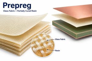
  • A proposed prepreg thickness may not be practical for normal production.
  • An impedance geometry may need adjustment once the actual laminate and copper thickness are confirmed.
  • A long through-hole via may leave an undesirable stub on a high-speed channel.
  • A complex stacked-microvia structure may add cost or reliability risk without being necessary.

This is where DFM goes beyond DRC. Design-rule checking determines whether a PCB follows a defined set of layout constraints, while manufacturing review determines whether those constraints can be reproduced consistently through drilling, plating, etching, lamination, surface finishing, assembly, and testing.

At EBest Circuit, our engineering review considers the released design together with its intended manufacturing process, including stackup, material, trace/space, copper thickness, via construction, controlled impedance, surface finish, and assembly requirements. AI may shorten the path to a completed layout, but the digital geometry still has to be converted into a stable production process.

AI-assisted PCB design compared with physical PCB manufacturability review

Why Does the AGI Era Need High-Speed PCBs?

The connection comes down to data movement. AI accelerators constantly exchange data with memory, CPUs, neighboring accelerators, storage, and network interfaces, so increasing computing power without sufficient interconnect bandwidth leaves expensive processors waiting for data.

High-speed standards already show the direction of travel. PCIe 7.0 supports 128 GT/s raw data rate and up to 512 GB/s bidirectional bandwidth through an x16 link, using PAM4 signaling. PCI-SIG lists AI/ML, high-performance computing, hyperscale data centers, and other data-intensive applications among the markets driving this bandwidth increase.

At these speeds, the PCB channel has to control more than basic connectivity. Engineers must account for:

  • Insertion loss
  • Impedance discontinuities
  • Crosstalk
  • Differential skew
  • Via transitions
  • Return-path continuity
  • Copper roughness
  • Dielectric loss

A fabrication variation that has little practical effect on a low-speed control board may consume meaningful signal margin on an AI accelerator or server motherboard, which is why high-speed hardware demands tighter control over materials, geometry, stackup, and vias.

High-speed interconnect paths between AI accelerator, memory, and SerDes interfaces

What Makes an AI High-Speed PCB Different From a Standard PCB?

There is no single specification for an “AI PCB.” The difference comes from what the board is required to carry. An accelerator board with high-speed serial interfaces has very different manufacturing requirements from a low-speed controller used elsewhere in the same server.

Design Area Conventional PCB AI / High-Speed PCB
Signal environment Often lower-speed Multi-gigabit interfaces common
Material Standard FR-4 often sufficient Low-loss laminate may be needed
Impedance Selected nets may be controlled Often critical across many channels
Stackup Standard construction possible More tightly tied to SI and PI
Routing density Low to moderate Dense BGA escape common
Via structure Through vias widely used HDI or back drilling may be required
Power demand Moderate Higher current density possible
Verification Electrical test Impedance and tighter process control may be added

Layer count alone does not define a high-speed PCB. A 20-layer board carrying slow control signals may have modest signal-integrity requirements, while a smaller board carrying a demanding SerDes interface can require much tighter material, geometry, and impedance control.

Which PCB Materials Are Suitable for AI and High-Speed Computing?

Material selection should begin with the channel loss requirement rather than the most expensive laminate available. Depending on the interface speed and routing architecture, suitable materials may include:

  • High-Tg FR-4
  • Low-loss FR-4
  • Panasonic Megtron families
  • Rogers laminates
  • Other low-Dk / low-Df systems

The lowest Df value is not automatically the right choice. Engineers should also consider:

  • Data rate
  • Channel length
  • Dielectric thickness
  • Impedance geometry
  • Copper profile
  • Glass weave
  • Thermal reliability
  • Lamination structure
  • Material availability
  • Cost

For shorter channels or less demanding interfaces, a good low-loss FR-4 system may already provide sufficient performance. Longer channels with tighter insertion-loss budgets may justify a more specialized laminate.

EBest Circuit supports high-Tg FR-4, Rogers, Megtron, and other project-specific low-loss materials. When the design is still being developed, confirming the laminate family and production stackup before routing is finalized can prevent later changes to trace width, spacing, or impedance geometry.

Multilayer PCB stackup illustrating low-loss material options for high-speed AI hardware

Why Is Controlled Impedance Critical for AI Server PCBs?

High-speed traces behave as transmission lines, so their impedance has to remain within the intended channel design. Typical targets may include 50 Ω single-ended, 90 Ω differential, or 100 Ω differential, although the correct value always comes from the interface specification.

Actual PCB impedance depends on several physical variables:

  • Trace width
  • Finished copper thickness
  • Differential-pair spacing
  • Dielectric thickness
  • Material Dk
  • Distance to the reference plane
  • Etching compensation

Controlled impedance is therefore both a design requirement and a manufacturing requirement. A nominal 100 Ω pair in CAD does not guarantee a 100 Ω result after fabrication; the final trace geometry needs to correspond to the actual production stackup.

For high-speed projects, EBest Circuit can review the stackup and impedance geometry before production and perform TDR impedance verification when required. The fabrication package should clearly identify the impedance target, tolerance, layer, material, and copper requirement so these parameters can be checked before the board enters production.

Why Are HDI and Advanced Vias Important for AI Accelerator PCBs?

Large processors, FPGAs, accelerators, and memory packages can place thousands of connections inside a compact BGA footprint. Conventional plated through-holes occupy routing space through the full board thickness, so denser packages may require more efficient breakout structures.

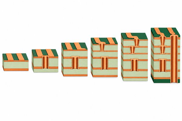
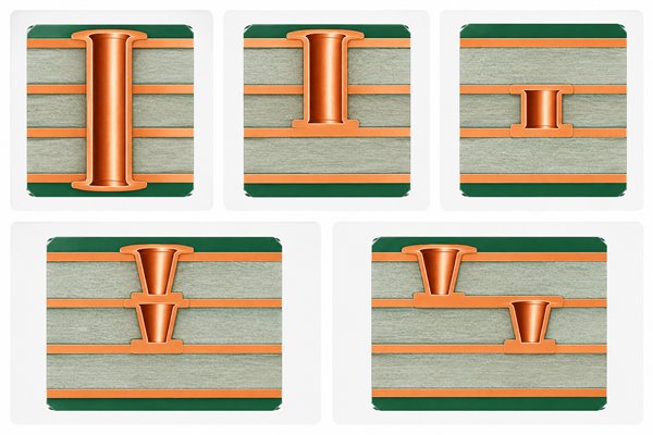
Depending on the architecture, HDI options can include:

  • Laser microvias
  • Blind and buried vias
  • Via-in-pad
  • Filled and plated vias
  • Staggered microvias
  • Stacked microvias
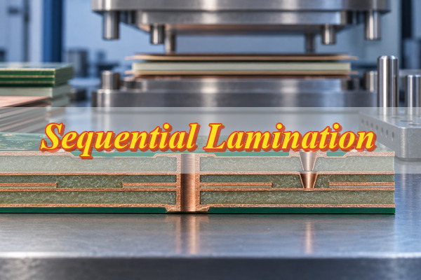
  • Sequential lamination

Shorter vertical transitions can reduce some of the electrical discontinuity associated with long through-hole vias. Where through-hole routing remains appropriate, back drilling may be used on selected high-speed channels to remove unused via stubs.

More complexity is not automatically better. Stacked microvias require additional processing and introduce their own reliability considerations, so if a staggered structure or conventional via construction satisfies the routing and signal requirements, adding another lamination cycle may offer little practical benefit.

EBest Circuit supports HDI, laser microvias, blind and buried vias, via-in-pad, and filled-via structures according to the actual BGA fanout and routing requirements.

Controlled impedance and HDI illustration showing blind vias, buried vias, via-in-pad, BGA breakout and an illustrative TDR curve

How Do Power and Thermal Demands Affect AI PCB Manufacturing?

High-speed signaling is only one challenge in AI hardware; power density is the other. Accelerator boards may need substantial current delivered through a compact area, which affects both stackup planning and copper distribution.

Common PCB considerations include:

  • Dedicated power and ground planes
  • Wider high-current copper paths
  • Dense power/ground via arrays
  • Low-inductance decoupling paths
  • Thermal vias
  • Local copper balancing
  • PDN planning
  • Warpage control

Power integrity and signal integrity also interact. A poor return path can affect a high-speed channel even when trace width and nominal impedance are correct, while supply noise can reduce the voltage and timing margin available to fast interfaces.

Manufacturing also has to account for copper distribution. Heavy or uneven copper can influence resin flow, lamination behavior, finished thickness, and board flatness. On high-layer-count server and accelerator boards, the stackup therefore has to balance signal routing, reference planes, power delivery, thermal behavior, and manufacturability rather than optimizing each factor independently.

What Should Engineers Check Before Sending an AI PCB to Production?

For an AI accelerator or high-speed computing board, a complete manufacturing package reduces avoidable engineering loops before fabrication.

Before release, confirm:

  • Final Gerber or ODB++ revision
  • Fabrication drawing
  • Layer stackup
  • Exact material grade or approved substitutions
  • Finished copper weight
  • Finished board thickness
  • Controlled-impedance table and tolerance
  • BGA pitch
  • Through/blind/buried/microvia structure
  • Via-in-pad and filling requirements
  • Back-drill requirements
  • Surface finish
  • Electrical and impedance testing
  • BOM and pick-and-place files for PCBA
  • Assembly drawing

The best time to resolve stackup, material, and impedance conflicts is before routing is fully locked. For technically demanding boards, an early fabricator review can prevent later changes to trace geometry, BGA breakout, or via structure after the production stackup has already been established.

AI PCB Manufacturing Case Studies from EBest Circuit

The following two representative cases show how the manufacturing priorities change between a dense AI accelerator PCB and a larger AI server or networking board.

Two AI PCB manufacturing case studies comparing an AI accelerator PCB and an AI server networking PCB

Case 1: High-Speed AI Accelerator PCB

Project: 16-layer low-loss PCB for an AI accelerator platform, with controlled differential impedance and dense BGA routing.

Specifications:

  1. Layer count: 16 layers
  2. Low-loss material / material brand: Panasonic Megtron 6
  3. Finished thickness: 2.0 mm
  4. Copper weight: 1 oz outer / 0.5–1 oz inner
  5. Controlled impedance: 50 Ω single-ended / 100 Ω differential
  6. Fine-pitch BGA: 0.5 mm pitch
  7. HDI / blind via / microvia / via-in-pad: Microvia + blind via + via-in-pad
  8. TDR testing: Yes
  9. Surface finish: ENIG
  10. Prototype quantity: 20 pcs
  11. PCBA / X-ray if applicable: SMT + BGA X-ray

This project mainly challenged dense BGA breakout, impedance consistency, and high-speed signal loss. The HDI structure provided more routing space around the fine-pitch package, while the low-loss material and controlled stackup supported stable high-speed transmission. It also shows why stackup and via structure should be confirmed with the fabricator before a dense accelerator layout is completely frozen.

Case 2: AI Server / High-Speed Networking PCB

Project: High-layer-count PCB for AI server and high-speed networking hardware, with high-speed SerDes routing and demanding power-distribution requirements.

Specifications:

  1. High layer count: 24 layers
  2. PCIe / high-speed SerDes related routing: PCIe / 112G SerDes
  3. Multiple controlled impedance values: 50 Ω / 85 Ω / 100 Ω
  4. Back drilling: Selected high-speed vias
  5. Large board size: 420 × 330 mm
  6. Tight finished thickness: 3.2 mm
  7. Low-loss stackup: Megtron 6
  8. High-current power/ground planes: Up to 2 oz
  9. Warpage control: ≤0.5%
  10. SMT + BGA X-ray: Yes
  11. Functional or electrical testing: Electrical test + TDR

This project placed more pressure on long high-speed channels, via-stub control, stackup stability, and board flatness. Back drilling and controlled impedance addressed the signal path, while copper balance and multilayer lamination control helped maintain dimensional stability on the larger board. Compared with the accelerator board, manufacturing control has to cover both electrical performance and the mechanical behavior of a large, thick multilayer PCB.

How Can EBest Circuit Support High-Speed PCB Manufacturing for AI Hardware?

EBest Circuit supports high-speed PCB and PCBA projects from manufacturing review through prototype and volume production. Instead of applying the same process to every AI-related board, we match the manufacturing route to the actual electrical, mechanical, and reliability requirements.

AI Hardware Requirement EBest Circuit Support
High-speed channels Controlled-impedance fabrication
Low channel loss High-Tg FR-4, Megtron, Rogers and other low-loss materials
Dense BGA breakout HDI, microvia and via-in-pad
Complex layer architecture Multilayer PCB manufacturing
Impedance verification TDR testing when specified
Production risk review DFM and stackup review
Dense SMT assembly SMT, AOI and X-ray
Prototype to production PCB + PCBA support

With more than 20 years of PCB and PCBA manufacturing experience and production support in China and Vietnam, we work with high-speed computing, networking, accelerator, and other data-intensive electronics.

The engineering objective is not to maximize layer count or specify the most expensive laminate. The better approach is to meet the required bandwidth, routing density, reliability, and production yield without adding process complexity that the design does not need.

What Does GPT-6 Astra Mean for the Future of PCB Engineering?

GPT-6 Astra’s KiCad demonstration gives a useful indication of how PCB design workflows may change. AI is likely to become more involved in tasks such as:

  • Initial placement and routing
  • Constraint checking
  • Documentation
  • Design comparison
  • Data preparation
  • Repetitive layout optimization

The manufacturing side remains physical. Copper still has to be etched, holes drilled and plated, and multilayer structures laminated within real process tolerances. Materials have actual Dk values, prepregs have available thicknesses, microvias have reliability limits, and finished boards still have to survive assembly and operate inside real electrical and thermal margins.

AI may become much faster at creating electronic designs, but turning those designs into reliable hardware will still depend on disciplined PCB engineering and manufacturing.

Frequently Asked Questions

1. Can GPT-6 Astra design a PCB?

Yes. OpenAI demonstrated GPT-6 Astra operating KiCad from an electronic schematic, performing component placement and PCB routing. This shows that a general-purpose AI system can now directly interact with professional PCB design software rather than only provide written design guidance.

2. Can AI design a manufacturable PCB?

AI can generate or assist with layouts that satisfy defined design rules, but manufacturability still depends on real fabrication constraints. Stackup, material availability, copper thickness, trace/space, impedance, via structure, plating, assembly, and reliability should still be reviewed before release.

3. Will AI replace PCB layout engineers?

AI is likely to automate some PCB layout and verification tasks, particularly repetitive work. Complex designs still require engineering judgment involving SI/PI, power delivery, component packaging, mechanical constraints, reliability, DFM, and manufacturing feedback.

4. Why do AI servers need high-speed PCBs?

AI servers contain accelerators, processors, memory, storage, and networking devices that exchange large volumes of data. The PCB carries many of those signals, so insertion loss, impedance, via transitions, return paths, crosstalk, and fabrication tolerance can affect high-speed channel performance.

5. What PCB materials are used for AI accelerator boards?

The material depends on the interface speed, channel length, loss budget, thickness, stackup, and cost. Options can range from high-Tg FR-4 to low-loss FR-4, Megtron, Rogers, and other low-Dk/low-Df systems. Not every AI accelerator PCB requires Rogers or another premium laminate.

6. What files should I send for a high-speed AI PCB quote?

For an accurate engineering review, provide the Gerber or ODB++ files, fabrication drawing, stackup, material requirement, copper weight, finished thickness, impedance table, drill/via information, and testing requirements. For assembly, also include the BOM, pick-and-place data, and assembly drawing.

If you are developing an AI accelerator PCB, AI server motherboard, high-speed computing board, HDI PCB, or controlled-impedance project, send your Gerber files, stackup, impedance requirements, BOM, and assembly specifications to sales@bestpcbs.com. Our engineering team can review the project before production and help confirm the appropriate material, stackup, via structure, impedance-control, and manufacturing approach.

You may also like

Hybrid Inverter PCBs: Design, Layout, and Manufacturing

September 3rd, 2026

Hybrid Inverter PCBs coordinate more power paths than a conventional grid-tied inverter board. They may receive energy from photovoltaic strings, charge or discharge a battery, form or follow an AC output, communicate with a battery-management system, and protect the product during faults or operating-mode changes. That combination makes board partitioning, insulation, switching-loop control, thermal design, and test access inseparable engineering decisions.

This guide explains how a hybrid inverter PCB is divided into functional blocks, what makes its layout difficult, and which manufacturing information should be settled before prototype release. The focus is the custom PCB and PCBA—not a replacement module selected only by inverter model number.

Hybrid Inverter PCBs inside an opened solar and battery inverter enclosure

What Are Hybrid Inverter PCBs?

A hybrid inverter PCB is part of the electronic platform that routes and converts energy among a photovoltaic array, battery, utility grid, and local loads. Unlike a simple DC-to-AC board, it must support multiple operating states: solar generation, battery charging, battery discharge, grid import, grid export where permitted, backup operation, and fault shutdown.

The phrase can refer to one integrated board or a coordinated set of boards. A compact unit may combine control, sensing, gate drive, auxiliary power, and portions of the power stage. Higher-power equipment often separates these functions so that heat, isolation, serviceability, and mechanical current paths can be managed independently.

How Does a Hybrid Inverter PCB Diagram Divide Power and Control?

A useful hybrid inverter pcb diagram begins with energy flow, not with component placement. The PV path normally includes input protection and an MPPT-controlled DC/DC stage. The battery path is often bidirectional because the same product must charge and discharge the battery. Both paths interact through a DC link before the DC/AC stage supplies the grid or protected loads.

Control, sensing, protection, and communications supervise every conversion stage. They measure voltage, current, and temperature; drive power switches; coordinate relays or contactors; communicate with the BMS; and move the system to a defined state when a reading becomes invalid.

Hybrid inverter PCB diagram showing PV, battery, DC-link, inverter, grid, load, control, sensing, and protection blocks

The diagram is an architecture map, not a manufacturing drawing. Before layout, each boundary must identify the maximum working and transient voltages, current direction, isolation requirement, switching frequency, signal bandwidth, fault energy, connector system, and cooling path. These inputs determine which functions can safely share a board.

Which Boards Belong in a Hybrid Inverter?

There is no universal board count. The right split depends on power level, enclosure geometry, service strategy, semiconductor package, cooling method, and certification path. The following division is common enough to guide an early design review.

Board or Module Primary Function Main PCB Concern
PV / MPPT power board Conditions photovoltaic input and tracks the operating point Switching-loop inductance, current path, sensing accuracy, and heat
Bidirectional battery board Controls battery charge and discharge Current reversal, protection coordination, bus impedance, and BMS interface
DC/AC inverter board Converts the DC-link energy into controlled AC Gate-drive loops, commutation paths, common-mode noise, and cooling
Control and communications board Runs control algorithms, measurements, protection logic, and communications Clean references, ADC routing, isolation, return paths, and firmware test access
Auxiliary supply / gate-driver board Provides isolated rails and switch control Isolation barrier, transformer parasitics, local decoupling, and propagation matching
DC-link / filter assembly Stores energy and filters switching components Low-inductance interconnect, mechanical fastening, ripple current, and clearance

A modular split can simplify cooling and replacement, but it adds connectors, harnesses, fastening tolerances, and interface failure points. An integrated hybrid inverter pcb board reduces interconnects, yet it concentrates heat and makes the high-energy and low-level circuits harder to separate. The tradeoff should be decided from electrical and mechanical requirements, not from board area alone.

How Should PV, Battery, DC-Link, and Grid Paths Be Partitioned?

Partition the assembly by energy domain and noise sensitivity. A practical floorplan keeps switching power cells compact while preventing high-dv/dt copper, high-di/dt loops, and hot components from crossing through measurement and communication areas.

  • Define current loops first. Mark the commutation loop for each switching stage and place its local capacitors before routing low-level signals.
  • Keep the DC link physically close to the power stage. Long bus paths add parasitic inductance and can increase overshoot and ringing.
  • Separate noisy and quiet grounds by function. Join them only through the intended measurement or isolation strategy; an arbitrary split plane can be as harmful as an uncontrolled shared plane.
  • Protect current and voltage sensing routes. Use deliberate differential routing, filtering, and reference returns so switch-node noise is not interpreted as real power-system behavior.
  • Plan precharge and discharge paths. Their components, connectors, and test points must be part of the physical architecture rather than added after the main bus is routed.
  • Review every state transition. Grid loss, battery connection, battery full/empty conditions, cold start, and protection trips can change current direction and common-mode conditions.

For a broader system-level view of sensing, switching, and protection, see our guide to power control systems. The hybrid inverter project should turn that system logic into explicit PCB domain boundaries.

What PCB Layout Decisions Control Switching Noise and EMI?

The schematic defines connections; the layout defines parasitic inductance, capacitance, and coupling. In fast-switching power converters, those unintended elements influence overshoot, gate stability, conducted noise, radiated noise, measurement error, and device stress.

  • Place gate drivers and their local supply capacitors close to the power-device control pins.
  • Keep gate and source/Kelvin return paths short, direct, and separated from high-current conductors.
  • Minimize switch-node copper to the area needed for current and heat, because a large high-dv/dt area can increase capacitive coupling.
  • Place high-frequency DC-link capacitors across the relevant power loop with the lowest practical connection inductance.
  • Route current-sense pairs together and away from switch nodes; do not share their quiet return with gate-drive or load current.
  • Give clocks, communications, and ADC references continuous, intentional return paths.
  • Reserve accessible probe points so ringing, gate voltage, bus voltage, and current-sense behavior can be measured safely during validation.
Hybrid inverter PCB layout showing short gate loop, isolation barrier, high-current path, and thermal via array

Moving from silicon IGBTs to faster SiC or GaN devices can expose layout weaknesses that were previously hidden. Faster edges can reduce switching loss, but the gate loop, common-source inductance, isolation capacitance, and measurement bandwidth need to be re-evaluated. A component substitution is not automatically a drop-in PCB change.

How Should High-Voltage Isolation Be Planned?

Working voltage alone is not enough to choose creepage, clearance, slots, or dielectric construction. The applicable end-product standard, insulation type, transient or impulse voltage, pollution degree, altitude, coating process, and material group all affect the required solution.

Map the isolation boundary across the complete assembly:

  • PCB copper, pads, vias, mounting holes, slots, and board edges
  • Transformers, optocouplers, digital isolators, relays, current sensors, and connectors
  • Heat sinks, screws, brackets, shielding, chassis, and cable routing
  • Contamination, condensation, coating coverage, and manufacturing tolerances

A routed slot can extend the surface path, but it does not automatically satisfy the air-clearance requirement. Solder mask is also not a universal substitute for qualified solid insulation. Our high-voltage PCB design guide explains why the final spacing must be tied to the actual insulation case instead of a generic voltage table.

Design-release rule: put working voltage, peak/transient voltage, insulation classification, altitude, pollution environment, CTI/material requirement, and governing product standard in the fabrication package. Do not ask the PCB supplier to infer them from the schematic.

How Do Copper and Thermal Design Affect Reliability?

Copper weight does not determine current capacity by itself. Conductor width and length, layer position, adjacent dielectric, via transitions, terminal contact, duty cycle, ambient temperature, enclosure airflow, heat-sink interface, and allowable temperature rise all influence the result.

Start with a loss map for semiconductor conduction and switching losses, magnetics, shunts, connectors, capacitors, relays, and copper paths. Then check the complete heat route from each source to copper planes, thermal vias, baseplate, heat sink, airflow, or enclosure. A large copper pour that ends in a thermally isolated region may spread heat locally without removing it from the assembly.

Heavy copper can reduce resistance and help spread heat, but it changes etching, lamination, drilling, plating, solder mask, copper balance, and reflow behavior. Our article on 4-layer heavy copper PCB design covers these manufacturing interactions in more detail.

For validation, measure the assembled unit under representative current, switching mode, battery charge/discharge direction, enclosure temperature, airflow, and duty cycle. Thermal images are useful for locating hot spots, but thermocouples or other calibrated measurements may be needed where emissivity or access makes an image misleading.

Which Materials and Stackups Suit Hybrid Inverter PCB Boards?

Most solar inverter pcbs and hybrid inverter control boards can begin with an FR-4-family construction, but the exact material system must be chosen from operating temperature, thermal cycling, insulation, CTI, copper weight, dimensional stability, CAF risk, and assembly profile. “High-Tg” alone does not describe all of those properties.

Design Need Construction Direction What Must Be Confirmed
Mixed control and moderate-power functions Multilayer FR-4 with deliberate reference planes and domain separation Stackup, dielectric system, copper distribution, isolation, and impedance where needed
High-current power paths Heavier copper, local bus structures, or separate power board Etched geometry, plating, terminal transitions, thermal rise, and manufacturability
High heat flux near power packages Thermal-via arrays, bonded heat spreader, metal-core sub-board, or ceramic option Electrical isolation, attachment method, solder reliability, and real cooling path
Fast control or communications Controlled multilayer return paths and impedance where the interface requires it Trace geometry, reference transitions, loss budget, and fabrication tolerance

A stackup should be reviewed with the fabricator before routing is frozen. Heavy outer copper can limit fine spacing; thick inner copper affects resin fill and lamination; mixed copper densities can worsen warpage; and isolation slots or large cutouts can weaken panel support. The optimum power board and control board may therefore use different constructions.

What Assembly Challenges Need Early DFM Review?

Hybrid inverter assemblies combine high-thermal-mass parts with dense control electronics. That creates competing stencil, placement, soldering, and inspection requirements. DFM should begin while component packages and mechanical interfaces can still change.

  • Large terminals and bus connections: confirm hole tolerance, copper connection, mechanical load path, fastening access, and soldering method.
  • Power packages: review exposed-pad geometry, void-sensitive joints, thermal vias, solder volume, heat-sink flatness, and mounting sequence.
  • Mixed thermal mass: evaluate whether one reflow profile can heat large power joints without overstressing nearby small components.
  • Tall and heavy parts: confirm placement clearance, polarity marking, adhesive or mechanical support, and vibration requirements.
  • Isolation areas: keep flux residue, markings, test pads, copper thieving, tooling features, and coating keep-outs from compromising the designed barrier.
  • Service connectors: check mating cycles, insertion forces, harness strain, and access after enclosure assembly.

Provide 3D mechanical data for heat sinks, busbars, capacitors, inductors, terminals, enclosure walls, and fasteners. A PCB can be electrically correct yet impossible to assemble without bending parts or loading solder joints.

How Should a Hybrid Inverter PCBA Be Tested?

Testing should be derived from the failure risks of each board. No single method proves conductor quality, solder integrity, measurement accuracy, isolation, communication, and system behavior at once.

  1. Bare-board verification: use netlist-based electrical testing or flying probe as appropriate, plus impedance, copper-thickness, and microsection checks where specified.
  2. Assembly process inspection: use visual inspection and AOI for presence, polarity, alignment, and visible joints.
  3. Hidden-joint inspection: apply X-ray where packages or power joints prevent adequate optical access.
  4. Low-energy bring-up: confirm rails, isolation interfaces, current-sense offsets, communications, programming, and protection logic before applying full bus energy.
  5. Functional verification: run the customer-defined fixture and limits for control states, I/O, relay sequencing, sensing, fault response, and communications.
  6. System validation: validate efficiency, temperature, EMI, grid behavior, battery transitions, surge/fault behavior, and product-standard requirements on a representative inverter assembly.
Engineer inspecting and functionally testing a hybrid inverter power-control PCBA

EBest Circuit can support AOI, X-ray inspection, functional testing, electrical/flying-probe testing, impedance testing, microsection inspection, and copper-thickness testing when they are defined for the project. Customer-owned firmware, fixtures, loads, pass/fail limits, and safety procedures should be identified before quotation so the production test scope is unambiguous.

What Common Failure Modes Should Be Designed Out?

Many inverter failures are system interactions that appear on the PCB. A useful design review traces the initiating condition, the electrical stress path, the thermal or mechanical consequence, and the test that can detect the weakness.

  • Gate ringing or false turn-on: commonly linked to loop inductance, common-source coupling, poor gate return, excessive edge rate, or isolation parasitics.
  • Current-sense instability: caused by switch-node coupling, weak reference routing, bandwidth mismatch, or shared high-current returns.
  • Hot terminals and neck-downs: created when a wide copper region funnels through a pad, via field, connector, fuse, or layer transition.
  • Isolation breakdown or tracking: associated with inadequate spacing, contamination, moisture, unreviewed slots, conductive hardware, or an incorrect insulation assumption.
  • Cracked power joints: driven by thermal cycling, package-to-board CTE mismatch, heavy components, heat-sink stress, or mounting tolerance.
  • Mode-transition resets: produced when auxiliary rails, ground references, communication links, or protection timing do not tolerate a sudden energy-flow change.

Do not treat a symptom such as “inverter PCB burned” as a root cause. Preserve fault logs, waveforms, failed parts, board location, operating mode, load, battery state, and environmental conditions for analysis.

What Files Are Needed for a Manufacturing Quote?

A complete RFQ lets the manufacturer evaluate board construction, assembly difficulty, inspection coverage, and material availability before price and lead time are committed.

  • Gerber or ODB++ fabrication data, NC drill files, netlist, stackup, finished copper requirements, board thickness, surface finish, controlled-impedance table, and dimensional drawing
  • BOM with manufacturer part numbers, approved alternates, do-not-substitute items, lifecycle concerns, and sourcing responsibility
  • Centroid/pick-and-place file, assembly drawings, polarity and orientation notes, stencil requirements, and special soldering instructions
  • Working and transient voltages, current and duty-cycle information, isolation classification, environmental conditions, applicable standards, and critical spacing dimensions
  • Heat-sink, busbar, terminal, enclosure, hardware, and 3D mechanical data with torque or flatness requirements where applicable
  • Programming files, functional-test procedure, fixture responsibility, test limits, required reports, sample approval plan, quantity, and delivery schedule

If the design is still evolving, mark assumptions and open items instead of hiding them. Early review of the solar inverter PCB manufacturing package can prevent a layout that works electrically but cannot be built or tested repeatably.

FAQ About Hybrid Inverter PCBs

What is the PCB in a hybrid inverter?

It is the printed circuit platform that supports power conversion, gate drive, sensing, protection, control, communications, or interface functions. A product may use one integrated PCB or several coordinated boards.

How is a hybrid inverter PCB different from a standard solar inverter PCB?

A hybrid design normally adds a battery energy path and the controls needed for bidirectional charging/discharging and multiple operating modes. That creates more interfaces, fault states, current directions, and transition conditions than a basic grid-tied PV inverter.

Can the power and control circuits share one PCB?

Yes, when the electrical, thermal, isolation, EMI, mechanical, and service requirements can all be met. Separating boards may be better at higher power or when different construction and cooling methods are needed.

Does every hybrid inverter need a heavy copper PCB?

No. Copper construction depends on current path, temperature rise, geometry, duty cycle, cooling, and assembly constraints. Busbars, separate power modules, or other structures may be preferable for some high-current paths.

Can SiC or GaN devices use the same layout as an IGBT design?

Not automatically. Faster switching can make gate-loop inductance, common-source inductance, isolation capacitance, switch-node coupling, measurement bandwidth, and EMI more critical. The PCB and gate-drive network should be reviewed with the selected device and operating conditions.

What determines the cost of Hybrid Inverter PCBs?

Major cost drivers include board size, layer count, copper construction, material system, via and slot requirements, controlled impedance, component availability, power-package assembly, inspection, fixtures, functional testing, order quantity, and required documentation. A complete package produces a more reliable quote than a schematic or photo alone.

How Can EBest Circuit Support Your Hybrid Inverter PCB Project?

At EBest Circuit, we support PCB design review, prototyping, fabrication, component sourcing, PCB assembly, and production transition for power and control electronics. Our relevant PCB options include multilayer, heavy copper, high-Tg, high-speed, impedance-control, metal-core, and ceramic constructions. Our documented quality and compliance credentials include ISO 9001:2015, IATF 16949, RoHS, REACH, and UL E502832; the applicable requirements and certification scope should still be confirmed for each program.

If you are preparing Hybrid Inverter PCBs for a new platform, we can review the board construction and assembly-sensitive details before the design enters production.

Send your Gerber or ODB++ data, BOM, stackup, quantity, operating voltage and current, isolation requirements, mechanical files, and test plan to sales@bestpcbs.com. We will review the fabrication, assembly, thermal, isolation, and test-sensitive details before quotation.
Tags: Hybrid Inverter PCBs, solar inverter pcbs, hybrid inverter pcb, hybrid inverter pcb board, hybrid inverter pcb diagram

You may also like

Power Divider vs Power Splitter: Key Differences for RF PCBs

September 3rd, 2026

power divider vs power splitter is a common search when an RF buyer needs to understand whether a circuit only has to distribute signal power or whether it also needs port isolation, balance, controlled impedance, and stable RF performance on the finished PCB.

In real RF projects, the answer is not only a vocabulary difference. The choice affects the circuit topology, expected insertion loss, port-to-port isolation, amplitude balance, phase balance, stackup, laminate choice, copper geometry, connector launch, and the information a PCB manufacturer needs before fabrication.

EBest Circuit does not sell standalone RF power divider or power splitter components. Our role is different: we support RF and high-frequency PCB fabrication, controlled impedance review, material selection review, ENIG and other PCB finishes, and SMT assembly when the customer releases a manufacturable PCB design for production.

power divider vs power splitter

Are Power Dividers and Power Splitters the Same?

Power dividers and power splitters are often used as if they mean the same thing, especially when people are simply describing one RF input being divided into two or more outputs. In many purchasing conversations, that wording overlap is normal.

For engineering work, the distinction matters. A power splitter usually means a simpler signal-splitting network. It may divide power, but it may not provide strong isolation between output ports. A power divider is often expected to provide better impedance matching, defined insertion loss, and isolation behavior, depending on the topology.

For a buyer, the useful question is not “Which word is technically perfect?” The useful question is “What does this RF circuit need the finished PCB to maintain?” If the circuit is only distributing a low-risk signal, a splitter-style structure may be enough. If the circuit must keep two RF paths balanced and isolated, the PCB has to support the divider requirements more carefully.

Buyer SituationUsually AcceptableReason
Simple signal distributionPower splitterLower isolation demand
Matched RF outputsPower dividerBetter balance control
Two outputs affect each otherPower dividerIsolation becomes important
Measured RF performance requiredPower dividerLoss, phase, and match must be controlled

Power Divider vs Power Splitter: Key Differences in RF Circuits

The main difference is how much RF behavior must be controlled after the signal is divided. A splitter can be enough when the application only needs to send one signal to multiple paths and the load interaction is not critical. A divider is more suitable when the outputs must remain matched, isolated, and predictable.

Insertion loss is one of the first differences buyers notice. Any two-way split has theoretical power division loss of about 3 dB before real-world losses are added. The PCB, connectors, copper, dielectric material, solder mask, and assembly can add more loss. For higher-frequency projects, those extra losses become easier to see in test results.

Isolation is another important difference. If one output port reflects energy or changes load condition, poor isolation can allow that change to disturb another output. In a divider circuit designed for isolation, the topology and PCB implementation work together to reduce that interaction.

Amplitude and phase balance also matter. In many RF systems, the two outputs are not judged only by whether signal appears at both ports. They are judged by how closely the two paths match. Small differences in trace width, dielectric thickness, connector launch geometry, via transitions, or electrical length can create measurable differences between outputs.

RF RequirementWhy Buyers Care
Insertion lossOutput signal strength
IsolationLess port interaction
Return lossBetter impedance match
Amplitude balanceMatched output levels
Phase balanceMatched signal timing
VSWRLower reflected energy

Power Divider vs Splitter Selection by RF Application

Application context decides whether a splitter is enough or a divider is safer. A lab test fixture, a monitoring point, or a simple distribution path may tolerate a basic splitter. A phased-array, antenna feed, RF front-end, test instrument, telecom module, or microwave signal path usually needs a divider structure with more controlled performance.

For buyers, the selection should start from the performance risk. If two outputs must be nearly equal, the board must protect symmetry. If one output load can change, isolation becomes more important. If the frequency is high enough that small geometry changes affect the result, the PCB stackup and controlled impedance notes must be treated as part of the RF design, not as a general fabrication detail.

Application NeedBetter DirectionPCB Impact
Basic signal splitSplitterStandard RF routing may be enough
Equal two-way outputDividerMatched branch geometry
Port isolation neededDividerTopology and layout must support isolation
High-frequency pathDivider or controlled splitterMaterial, impedance, and launch details matter
Measured RF boardDividerCoupons, reports, and tolerances may be required

This is why an RF PCB buyer should send more than Gerber files when requesting fabrication. Stackup, material, impedance targets, copper weight, solder mask preference, connector type, and test requirements help the manufacturer understand what must be controlled before production starts.

RF Power Divider vs Splitter Parameters That Change PCB Requirements

The RF parameters decide how sensitive the PCB will be. A low-frequency or low-risk splitter may be forgiving. A divider used in a measured RF path is much less forgiving because the board structure becomes part of the circuit.

Frequency is the first driver. As frequency rises, dielectric thickness, Dk stability, copper roughness, trace width, via geometry, and connector launch shape become more important. A small change that does not matter on a simple digital board can change RF behavior on a divider or splitter board.

Power level also matters. Higher power may require wider conductors, thermal consideration, copper thickness review, and spacing checks. If the board is used in a compact RF module, heat, insertion loss, and connector placement may all affect the final build.

Port count changes manufacturing sensitivity. A two-way structure is easier to keep symmetrical than a four-way or eight-way structure. More branches mean more chances for small geometry differences to affect amplitude balance or phase balance.

ParameterPCB Detail Affected
FrequencyLaminate, Dk, trace geometry
Power levelCopper, spacing, heat
Port countSymmetry and branch matching
Isolation targetTopology-sensitive layout
Phase balanceElectrical length control
Connector typeLaunch geometry and grounding

Before quotation, buyers should share the released stackup, controlled-impedance notes, material requirement, copper requirement, surface finish, connector type, and any impedance test or RF test expectation. This allows the manufacturing review to focus on the details that can actually affect the finished board.

RF PCB Material Choices for Divider and Splitter

Material choice affects loss, impedance stability, and repeatability. FR-4 may be acceptable for lower-frequency or less sensitive splitter applications. For higher-frequency divider or splitter circuits, RF laminates such as Rogers, Taconic, Isola, or Shengyi high-frequency materials may be considered depending on frequency, loss target, cost, and availability.

The material decision should be made by the customer’s RF design team. From the manufacturing side, EBest Circuit can review whether the selected material, Dk, dielectric thickness, copper, finished thickness, and surface finish are clearly defined for production.

For divider and splitter PCBs, laminate consistency matters because the signal path is not only a copper trace on a board. The dielectric under or around the trace is part of the transmission-line structure. If the Dk, dielectric thickness, or copper geometry changes, the impedance and electrical length can change with it.

Material FactorBuyer Impact
Dk stabilityMore predictable impedance
Df / loss tangentLower RF loss
Dielectric thicknessTrace width and impedance control
Copper typeLoss and etching result
Pressed stackupRepeatability across builds
Surface finishSolderability and RF interface reliability

EBest Circuit can support RF/high-frequency PCB projects using materials such as Rogers, Taconic, Isola, Shengyi, Arlon, and similar laminate systems when the project files define the requirement clearly.

power divider vs power splitter

Controlled Impedance in Divider and Splitter RF PCBs

Controlled impedance in a divider or splitter RF PCB does not always mean every RF trace is 50 Ω. The required impedance depends on the circuit topology. In a typical two-way Wilkinson divider, for example, the input and output ports are usually 50 Ω, while the quarter-wave branch lines are about 70.7 Ω.

The most sensitive areas are the input trace, split point, branch lines, output paths, via transitions, and RF connector launches. Even when two output traces look symmetrical, differences in trace width, dielectric thickness, via structure, or electrical length can affect return loss, insertion loss, amplitude balance, and phase balance.

For fabrication, impedance is controlled by finished trace width, copper thickness, dielectric thickness, laminate Dk, transmission-line structure, etching variation, plating result, solder mask condition, and reference-plane continuity.

A common controlled-impedance tolerance is ±10%, while tighter RF designs may specify ±5%, depending on frequency, material system, line geometry, and customer requirements. For a nominal 50 Ω line, ±10% corresponds to approximately 45–55 Ω.

The manufacturing files should identify the controlled traces, target impedance, signal layer, reference plane, material, dielectric thickness, copper thickness, tolerance, and any coupon or test-report requirement. This avoids a common RF PCB problem: the Gerber geometry says one thing, while the stackup or impedance note says another.

EBest Circuit can review the released PCB data to confirm that the stackup, materials, copper, and impedance requirements are clearly defined for fabrication. The RF circuit target remains with the customer’s design team, while our role is to ensure those requirements can be built consistently.
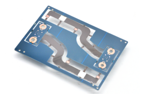
power divider vs power splitter

How EBest Circuit Supports RF PCB Builds for Divider and Splitter

EBest Circuit supports divider and splitter PCB projects as RF/high-frequency PCB builds, not as off-the-shelf RF component sales. Buyers provide the released PCB design, stackup, material notes, impedance targets, drawings, and assembly files. We review the manufacturing side before production.
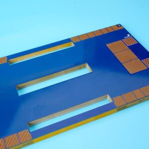
For fabrication, we can review RF laminate selection, finished thickness, copper structure, controlled-impedance requirements, ENIG or other surface finish requirements, solder mask notes, via structures, panelization, and connector-related manufacturing details.

For assembly, EBest Circuit can support SMT and THT requirements when the RF PCB design includes components, SMA connectors, shielding parts, or mixed assembly. The useful result for the buyer is a clearer path from released RF design data to buildable PCB or PCBA production.

Buyer SendsEBest Circuit Reviews
Gerber and drill filesFabrication feasibility
Stackup drawingLayer and dielectric consistency
Impedance tableTarget values and tolerances
Material notesLaminate and copper requirements
BOM and CPLSMT assembly readiness
Connector drawingsLaunch and footprint clarity

If files are incomplete, the buyer gets fewer surprises when the open items are clarified before fabrication. If the files are consistent, the project can move into production with less risk of stackup, material, or impedance misunderstanding.

RF PCB Case Study for a Power Divider Project

A two-way RF power divider project submitted to EBest Circuit required controlled-impedance transmission lines and closely matched output paths. The PCB used Shengyi S1000-2 TG170 material, a finished thickness of 1.60 mm ±10%, ENIG surface finish, and a specified 50 Ω trace with a 0.19 mm line width on the inner signal layer.

The divider had one RF input and two outputs. The input and output transmission lines were designed for 50 Ω, while the quarter-wave divider branches used approximately 70.7 Ω impedance. The design also specified an amplitude balance within ±0.3 dB and a phase balance within ±3° between the two outputs. SMA connectors were used for the RF input and output interfaces.

Problem

During the manufacturing review, the specified 50 Ω trace geometry did not fully match the released stackup information. For this power divider, the issue was important because the input, 70.7 Ω branch sections, and two 50 Ω output paths depended on defined transmission-line geometry.
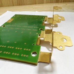
If the board had entered production without clarification, changes in dielectric thickness or finished trace geometry could have shifted the impedance and created differences between the two RF paths, potentially affecting return loss, insertion loss, amplitude balance, and phase balance.

Solution

Before fabrication, EBest Circuit reviewed the laminate, copper structure, dielectric thickness, finished board thickness, 50 Ω traces, and 70.7 Ω branch-line requirements with the customer. The production stackup and impedance parameters were aligned before manufacturing.

The two output paths and SMA launch areas were also reviewed for consistent RF geometry and reference-plane conditions.

The project required turnkey SMT assembly as well. After assembly, each board was carefully cleaned, with no solder balls or other visible contamination allowed on the PCB surface.

Result

The production stackup and controlled-impedance structure were confirmed before fabrication, reducing the risk of impedance deviation between the input, divider branches, and two output paths.

By resolving the manufacturing data before production, the PCB could be built around the intended 50 Ω and 70.7 Ω transmission-line structures while maintaining the geometry required for consistent RF output performance.

power divider vs power splitter

FAQs About Power Divider vs Power Splitter

Is a power divider the same as a power splitter?
They are often used interchangeably in casual RF discussions, but a power divider usually implies more defined matching, isolation, and balance behavior. A splitter may simply divide signal power with less isolation.

When is a power splitter enough?
A splitter may be enough for simple signal distribution, lab monitoring, low-risk test paths, or applications where output-to-output interaction is not critical.

When should buyers use a power divider?
A power divider is more suitable when the outputs need controlled matching, isolation, amplitude balance, phase balance, or stable performance across a defined frequency range.

Does every divider or splitter RF PCB use 50 Ω traces?
No. Many RF ports are 50 Ω, but some divider branches may use other impedance values. A two-way Wilkinson divider, for example, commonly uses about 70.7 Ω quarter-wave branch lines.

What PCB information should be provided for a divider or splitter board?
Send Gerber files, drill files, stackup, material requirement, copper thickness, controlled-impedance table, surface finish, connector information, and any impedance coupon or test-report requirement.

Can EBest Circuit design the RF divider or splitter circuit?
The RF circuit design and performance target should come from the customer’s design team. EBest Circuit can review the released files for PCB manufacturability, stackup clarity, material definition, impedance requirements, fabrication, and assembly readiness.

Can EBest Circuit manufacture RF divider and splitter PCBs?
Yes, when the customer provides released manufacturing data. EBest Circuit can support RF/high-frequency PCB fabrication, controlled-impedance review, surface finish, and SMT assembly where required.

If you are comparing power divider vs power splitter requirements for an RF PCB project, send your Gerber files, stackup, impedance notes, material requirement, BOM, CPL, and quantity to sales@bestpcbs.com. EBest Circuit can review whether the released data is clear enough for RF PCB fabrication and assembly before production starts.

You may also like

What Is Solder Paste Inspection in PCB Assembly?

September 3rd, 2026

What is solder paste inspection? Solder paste inspection, or SPI, checks the deposits printed onto PCB pads before components are placed. A 3D SPI system measures deposit height and shape to calculate area, volume, and position. These measurements help identify printing problems while the board can still be corrected before placement and reflow.

The useful question is not simply whether the machine displays “pass.” It is whether the inspection program measures the right deposits, uses a suitable reference, and applies limits that have been validated for the assembly. A passing print is one process checkpoint—not proof that every finished solder joint will be reliable.

What Is Solder Paste Inspection? Optical inspection of paste deposits before component placement

Where Does SPI Fit in the PCB Assembly Line?

SPI normally sits after stencil printing and before pick-and-place. At this point, the inspection target is the printed paste—not a mounted component or a solidified solder joint.

  1. Print: a squeegee transfers paste through stencil apertures onto the pads.
  2. Inspect: SPI checks the deposits against the programmed print requirements.
  3. Place: components are positioned on accepted prints.
  4. Reflow: the assembly follows a qualified thermal profile.
  5. Inspect and test: later checks evaluate placement, accessible joints, hidden features where applicable, and electrical performance.

Finding a printing error early can avoid placing components onto a defective print. It does not remove the need to control placement accuracy, paste condition, reflow, or downstream testing.

SMT process order: print, SPI, placement, reflow and AOI

Solder Paste Inspection Process

The solder paste inspection process begins with a board-specific program. Accurate machine measurements cannot compensate for an incorrect pad map, reference volume, or revision.

  • Load the correct data: match PCB revision, paste-layer data, stencil revision, and component requirements.
  • Register the board: use the configured fiducials and board orientation to locate inspection regions.
  • Establish the surface reference: identify the local board or pad baseline used for height measurements.
  • Measure and classify: compare each deposit with the appropriate target and limits.
  • Review exceptions: separate actual print defects from alignment, reference, or recipe errors.
  • Record the disposition: release, hold, or clean and reprint under the approved process.

Programming should distinguish solder paste openings from copper and solder mask features. Our explanation of solder mask and solder paste layers covers why these data sets are not interchangeable.

Solder Paste Inspection Parameters

The main solder paste inspection parameters are height, area, volume, and offset. Reading them together is more useful than treating any one number as a complete verdict.

Parameter Measurement Typical units
Height Deposit elevation above the selected reference surface µm
Area Detected deposit footprint in the board plane mm² or percentage
Volume Paste volume calculated from measured shape mm³ or percentage
Offset Deposit displacement from the programmed target µm in X and Y

A wide, shallow deposit may have an acceptable-looking footprint but insufficient volume. Conversely, a tall deposit does not necessarily contain the intended total volume if its footprint is small. Offset can also matter even when volume is close to target: the paste must be positioned where the termination and pad need it.

Solder paste deposit height, footprint area and three-dimensional volume

Example—not an acceptance limit: assume a rectangular stencil aperture is 0.30 mm × 0.50 mm in a 0.10 mm thick stencil. Its theoretical aperture volume is 0.015 mm³. A measured deposit of 0.012 mm³ represents 80% transfer efficiency relative to that aperture volume. Whether it is acceptable depends on the validated assembly requirements; 80% is not automatically a pass or fail.

Before interpreting a percentage report, ask what “100%” means. It may refer to theoretical aperture volume or a configured nominal target. Results from different programs are not directly comparable until their reference definitions are aligned.

How Does 3D SPI Measure the Paste?

3D SPI reconstructs the deposit surface using optical measurement. Depending on the equipment, this can involve projected light patterns or laser-based profiling. The measured surface is compared with a reference plane to calculate deposit geometry.

A 2D image can reveal a footprint or visible bridge, but it does not independently provide a full height map. That difference matters when two deposits look similar from above yet contain different amounts of paste.

Board warpage, surface reflectivity, shadows, and the choice of reference regions can influence the measurement. Multiple illumination directions and local height-reference methods are examples of equipment features used to address these issues. Their availability and performance are machine-specific; “3D” alone does not establish measurement capability.

For a demanding package, check repeatability on the actual board and deposit geometry. A brochure resolution number is not the same as demonstrated measurement accuracy in production.

A practical measurement study separates repeated scans of the same print from scans after the board is unloaded and reloaded. The first tests short-term measurement consistency; the second also exposes registration and handling effects. If those variations are large relative to the proposed tolerance, the process team should resolve the measurement problem before using the results for fine printer adjustments.

Solder Paste Inspection Tolerance

Solder paste inspection tolerance should be set around the needs of each deposit group and validated against assembly results. One percentage window should not be assumed suitable for every pad on a mixed-technology board.

Start with the stencil design, paste characteristics, package geometry, and printing process. Then use trial builds and downstream findings to establish limits that separate acceptable variation from prints likely to cause trouble.

  • Group deposits with comparable aperture geometry and assembly requirements.
  • Confirm that height and volume references remain stable across the board.
  • Assess measurement variation before tightening a tolerance.
  • Correlate marginal prints with placement, reflow, and final inspection results.
  • Control program revisions when the stencil, paste, board finish, or package changes.

Repeated false calls are a reason to investigate the measurement and recipe, not automatically widen every limit. Equally, a low rejection count is not evidence of a capable process if the limits are too broad to identify meaningful variation.

Windowed apertures for a large thermal pad need particular care in the recipe. Several separate deposits may belong to one component land. Decide whether acceptance is evaluated by individual window, a combined region, or both, and document that choice. Comparing the combined volume with a target intended for one window would produce a misleading result even if the optical measurement itself were correct.

Solder Paste Inspection Defects

Solder paste inspection defects include missing deposits, insufficient or excessive paste, misplaced deposits, and paste connecting regions that should remain separate. These are printing conditions, not final solder-joint diagnoses.

Conceptual missing paste, low-volume paste and paste bridge before component placement
  • Missing or low-volume paste: investigate blocked apertures, release behavior, paste condition, and print settings.
  • Excess paste: check aperture design, stencil contact, support, and the printing setup.
  • Deposit offset: review alignment, fiducial recognition, board movement, and registration.
  • Paste bridging or smearing: examine stencil underside contamination, separation behavior, support, and material handling.

The pattern helps narrow the investigation. A problem confined to one aperture differs from a whole-board shift or a gradual trend across many prints. SPI identifies what changed; confirming the cause still requires examining the printing process.

Do not label a print as a “cold solder joint.” That term describes a soldering outcome, whereas SPI takes place before solder has reflowed. The later thermal and metallurgical conditions have not yet occurred.

What Should Happen After an SPI Failure?

Hold the affected board before component placement and verify the call. Review the image or height map, the failed value, the target, and the program revision before making a disposition.

If the print is genuinely unacceptable, follow the approved cleaning and reprinting procedure for the board and paste system. Do not assume that adding paste by hand produces the same controlled deposit as a qualified printing process.

Then address recurrence: check the stencil, board support, print alignment, underside cleaning, paste handling, and relevant printer settings. After a correction, inspect a new print and verify that the original problem is resolved without introducing a different one.

For repeated failures around small apertures, review the SMT stencil as well as the machine settings. An inspection threshold cannot repair an aperture design that does not release paste consistently.

How Is SPI Different from AOI?

SPI evaluates the print before placement; AOI evaluates visible features at its configured inspection stage. They answer different questions and should not be treated as substitutes.

Inspection Typical stage Main target
SPI After paste printing Deposit geometry and position
Pre-reflow AOI After placement, where used Visible component presence and placement
Post-reflow AOI After soldering Visible component and joint features

Hidden solder connections may require other inspection methods, and electrical defects require appropriate testing. Neither an SPI pass nor an AOI pass proves every functional requirement. For the later optical stage, see our guide to AOI in PCB manufacturing.

How Can SPI Data Improve Printing Control?

Trend data can reveal drift that an isolated pass/fail result hides. Track comparable deposit groups by board, print sequence, stencil revision, and relevant process events rather than averaging unrelated pads into one reassuring number.

For example, a consistent directional offset may justify checking alignment, while falling volume in a particular aperture group may prompt a stencil-release investigation. Compare the trend with cleaning cycles and setup changes before assigning a cause.

Some printer and SPI combinations support integrated feedback. Such a connection needs compatible equipment, validated correction rules, and limits on what the system may adjust. It should not be assumed present on every SMT line, and it should not turn an unresolved measurement problem into an automatic printer correction.

What Should an SPI Report Contain?

A useful report lets an engineer trace a result to the board, deposit, program, and disposition. A green dashboard without that context is difficult to investigate later.

  • Board or panel identifier, inspection time, and product revision.
  • SPI program revision and the applicable pad or deposit group.
  • Measured values, units, nominal references, and acceptance limits.
  • Images or height maps for reviewed exceptions.
  • Release, hold, reprint, or other approved disposition.
  • Relevant process changes and links to downstream inspection or test records.

Specify the required records before production if they are part of your quality agreement. Retention, serialization, and reporting formats should be agreed for the project rather than assumed from the presence of an SPI machine. Our overview of PCB testing explains how inspection fits into a broader verification plan.

How Can EBest Circuit Support Your PCB Assembly Inspection Plan?

At EBest Circuit, we provide PCB fabrication and PCBA assembly support, including solder paste inspection within our SMT capabilities. We can review your board data, component requirements, and inspection expectations together so the manufacturing and verification plan matches the assembly.

If your starting question is what is solder paste inspection, the next step is to identify which print characteristics matter for your components and which records your project needs.

Send your Gerber files, BOM, placement data, quantity, and inspection or traceability requirements to sales@bestpcbs.com. We will review the assembly scope with you, including any package-specific checks that need to be agreed before production.

You may also like

Soldering Temperature Guide for PCB and Electronics

September 3rd, 2026

Choosing the right soldering temperature is not as simple as setting an iron to one number and using it for every joint. For most electronics work, a soldering iron tip is commonly set somewhere around 315–350°C (599–662°F) for leaded solder and 340–370°C (644–698°F) for common lead-free solder. These are practical starting ranges rather than universal limits.

The correct setting also depends on solder alloy, PCB copper area, tip geometry, component size, flux activity, and how quickly the soldering station can replace lost heat. A small SMD pad may solder cleanly near the lower end of the range, while a connector tied to a large ground plane may need a larger tip, preheating, or a modest temperature increase.

Soldering temperature guide for PCB and electronics showing a temperature-controlled soldering station and PCB hand soldering

What Is the Best Soldering Temperature for Electronics?

For general electronics soldering, about 320–350°C is a useful starting range for leaded solder, while 340–370°C is more typical for lead-free solder.

The temperature should be high enough to heat the pad, component lead, and solder quickly, but not so high that flux burns away before the joint forms.

A practical starting point is:

  • Fine electronic wiring or small pads: 300–330°C
  • General PCB work with leaded solder: 320–350°C
  • General PCB work with lead-free solder: 340–370°C
  • Large connectors or high-copper areas: often near the upper end of the range, preferably with a larger tip or PCB preheating

The best soldering temperature is therefore the lowest setting that can bring the entire joint to soldering temperature within a short, controlled contact time.

If the iron must remain on the joint for a long time, simply using a lower temperature is not necessarily gentler. Extended heating can transfer more total energy into the PCB and component than a slightly hotter tip used briefly.

Soldering Temperature Chart for PCB and Electronics

The following soldering temperature chart provides practical starting values for common electronics work.

Application Solder / Process Melting or Liquidus Temperature Practical Starting Setting
General PCB hand soldering Sn63/Pb37 183°C 320–350°C
General PCB hand soldering Sn60/Pb40 About 183–190°C 320–350°C
Lead-free PCB soldering SAC305 About 217–220°C 340–370°C
Fine SMD hand soldering Leaded About 183°C 300–330°C
Fine SMD hand soldering Lead-free About 217–220°C 320–350°C
Large PCB connector Leaded About 183–190°C 340–370°C*
Large PCB connector Lead-free About 217–220°C 350–380°C*
Leaded hot-air rework Process dependent About 300–350°C display setting*
Lead-free hot-air rework Process dependent About 320–380°C display setting*
Leaded desoldering SnPb About 183–190°C 330–370°C*
Lead-free desoldering SAC-type alloy About 217–220°C 350–390°C*

*These values depend strongly on thermal mass, equipment calibration, nozzle or tip size, airflow, and preheating.

The table should be treated as a setup reference rather than a process specification. The actual solder joint temperature is different from the temperature shown on the soldering station.

Soldering temperature chart for leaded, lead-free, SMD, hot-air rework and desoldering

Why Is Soldering Iron Temperature Higher Than the Solder Melting Point?

A soldering iron is normally set far above the solder’s melting point because heat must travel from the heater through the tip and into the complete joint.

For example, Sn63/Pb37 solder melts at 183°C, but setting an iron to 183°C would usually provide very little thermal margin. As soon as the tip touches a copper pad, heat begins flowing into:

  • the copper track,
  • plated through-hole barrel,
  • component lead,
  • nearby copper planes,
  • and the PCB laminate.

The tip surface can cool substantially during this transfer.

This is why melting temperature and soldering iron temperature are not interchangeable measurements.

Three temperatures are especially easy to confuse:

  • Solder melting temperature: where the alloy changes state.
  • Joint temperature: the temperature actually reached by the pad, lead, and solder.
  • Tip set temperature: the value selected on the soldering station.
A good soldering station compensates quickly when the tip loses heat. A weak station may show 350°C on the display yet struggle on a large ground connection because its heater cannot restore tip temperature fast enough.

Diagram showing why soldering iron tip temperature is higher than solder melting point due to heat flow into the PCB

What Soldering Temperature Should You Use for 60/40 and 63/37 Solder?

For 60/40 and 63/37 tin-lead solder, approximately 320–350°C is a practical hand-soldering starting range for normal PCB work.

The two alloys behave slightly differently.

Sn63/Pb37 is eutectic. It changes from solid to liquid at approximately 183°C without a significant pasty range. This makes the joint relatively easy to form and inspect during hand soldering.

Sn60/Pb40 begins melting at approximately 183°C and becomes fully liquid at around 190°C. It passes through a short plastic or pasty range during cooling.

For both alloys:

  • Small pads can normally use the lower end of the temperature range.
  • Larger terminals may require 340–350°C or slightly more.
  • Large ground planes should first be addressed with a larger tip or preheater rather than excessive temperature.
  • Good flux activity can reduce the time required to achieve complete wetting.

The difference between 60/40 and 63/37 is important, but PCB thermal mass usually has a greater effect on the required iron setting.

What Is the Best Soldering Temperature for Lead-Free Solder?

For common lead-free electronics solder such as SAC305, 340–370°C is a practical starting range for hand soldering.

Lead-free solder typically has a higher melting temperature than traditional SnPb solder. SAC305, for example, has a liquidus temperature around 217–220°C.

However, its higher working temperature does not mean every lead-free joint should automatically be soldered at 380°C or 400°C.

A better approach is to start around 340–350°C and increase only when the joint cannot reach temperature quickly enough.

Lead-free soldering also benefits from:

  • an appropriately sized chisel or bevel tip,
  • a station with good thermal recovery,
  • active flux,
  • clean and well-tinned tip surfaces,
  • and PCB preheating for large thermal masses.

Lead-free processes can oxidize tips faster, so continuously increasing temperature to compensate for a poorly wetted or oxidized tip usually makes the situation worse.

Leaded versus lead-free solder comparison showing melting point and typical soldering iron settings

What Soldering Iron Temperature Should You Use for PCB Work?

For most PCB hand soldering, about 320–350°C for SnPb solder and 340–370°C for lead-free solder provides a useful starting window.

The PCB construction determines how much heat the joint absorbs.

A small pad on a standard two-layer FR-4 board may reach soldering temperature almost immediately. The same component lead connected to a multilayer ground plane can pull heat away from the tip much faster.

Pay particular attention to:

  • Ground and power planes: internal copper spreads heat away from the joint.
  • Heavy copper PCB: thicker copper requires more thermal energy.
  • Large plated through-holes: the barrel conducts heat through the board thickness.
  • Large connectors: metal housings and thick pins act as heat sinks.
  • Thermal vias: arrays of vias can transfer heat into internal or opposite-side copper.
  • Metal-core boards: heat can leave the soldering area rapidly.

When a PCB joint is difficult to solder, using a larger tip with better contact area is often more effective than immediately turning the station hotter.

What Is the Proper SMD Soldering Temperature?

For small SMD hand soldering, about 300–330°C for leaded solder and 320–350°C for lead-free solder is often sufficient when the tip size and flux are appropriate.

Small components have little thermal mass, so they normally do not require the same thermal input as a large connector.

For packages such as 0402, 0603, SOIC, or fine-pitch IC leads, temperature control matters because the pad area is small and repeated heating can weaken the pad-to-laminate bond.

For cleaner SMD work:

  • Use a tip that matches the pad geometry.
  • Apply flux before touching the joint.
  • Keep contact time short.
  • Avoid pressing the tip into the pad.
  • Allow the joint to cool before repeated rework.
  • Use hot air or controlled reflow methods when a package cannot be heated evenly with an iron.

A high temperature is not automatically faster if the tip is too small to transfer heat efficiently.

What Hot Air Soldering Temperature Should You Use for PCB Rework?

For PCB hot-air rework, roughly 300–350°C for leaded assemblies and 320–380°C for lead-free assemblies can be used as initial station settings, but airflow and PCB preheating are equally important.

A hot-air station does not behave like a soldering iron. The displayed temperature is the heater or calibrated air temperature, not necessarily the temperature at the solder joint.

Actual heating depends on:

  • nozzle diameter,
  • airflow,
  • nozzle-to-board distance,
  • component size,
  • board thickness,
  • copper distribution,
  • surrounding components,
  • and whether the PCB is preheated.

A thick multilayer PCB may require a higher displayed air temperature than a thin board, even when the target solder joint temperature is similar.

For large BGAs, QFNs, shielded modules, or high-copper boards, preheating the PCB reduces the temperature difference between the rework area and the rest of the board. This generally allows gentler top-side heating and reduces local thermal stress.

What Desoldering Temperature Should You Use?

For desoldering, about 330–370°C for leaded joints and 350–390°C for lead-free joints is a reasonable starting range, depending on board construction and the removal method.

Old solder can be more difficult to remove because of oxidation, contamination, or poor remaining flux activity.

Before raising the temperature, try:

  • applying fresh flux,
  • adding a small amount of fresh solder,
  • using a wider desoldering tip,
  • improving contact with the joint,
  • preheating large multilayer boards,
  • or using a powered desoldering tool for plated through-holes.

Adding fresh solder may seem counterintuitive, but it introduces active flux and improves heat transfer into an old joint.

Extra care is required on plated through-holes. Excessive temperature combined with prolonged heating can damage pad adhesion or the connection between the hole barrel and internal copper layers.

Hot-air rework and desoldering temperature guide for PCB repair

What Factors Change the Proper Soldering Temperature?

The proper soldering temperature is primarily determined by how efficiently heat moves from the tool into the solder joint.

The most important variables are:

  • Solder alloy: lead-free alloys generally require higher process temperatures than SnPb alloys.
  • Copper area: large pads, planes, and heavy copper remove heat rapidly.
  • Tip geometry: a larger contact surface transfers energy more efficiently.
  • Station power and recovery: higher heater capacity helps maintain tip temperature under load.
  • Flux condition: active flux improves wetting and reduces the time needed to form the joint.
  • Component thermal mass: connectors, switches, shields, and large terminals absorb more heat.
  • PCB thickness: thick multilayer boards usually require more thermal energy.
  • Preheating: raising the overall PCB temperature can reduce the heat demanded from the soldering tool.
  • Contact time: temperature and dwell time must be considered together.

A station temperature therefore cannot be selected from solder alloy alone. Two assemblies using SAC305 may require noticeably different settings because one has small SMD pads while the other has a large connector tied to a power plane.

PCB factors that change soldering temperature including ground planes, heavy copper, thermal vias and connector size

How Can You Tell If the Soldering Temperature Is Too High or Too Low?

The condition of the joint often shows whether the soldering temperature or heat-transfer setup needs adjustment.

Temperature Too Low / Heat Transfer Too Weak Temperature Too High / Heating Too Aggressive
Solder does not wet the pad easily Flux burns or smokes excessively
Joint looks dull, uneven, or incomplete Tip oxidizes quickly
Solder forms a ball instead of spreading PCB surface discolors
Long contact time is required Pads may loosen or lift
Large joints refuse to flow Plastic connectors may deform
Excessive pressure is needed with the iron Components experience unnecessary thermal stress

A cold-looking joint does not always mean the temperature setting is too low. An oxidized tip, insufficient flux, a very small tip, or a large ground plane can produce similar symptoms.

Likewise, a joint that takes too long at 350°C may be improved by switching from a fine conical tip to a larger chisel tip instead of increasing the iron to 400°C.

FAQs About Soldering Temperature

Is 350°C too hot for PCB soldering?

No. Around 350°C is a common working temperature for many PCB soldering operations, particularly lead-free work or joints with moderate thermal mass. For small heat-sensitive pads, a lower setting may be more appropriate.

What is the normal soldering temperature for electronics?

A typical starting range is approximately 320–350°C for leaded solder and 340–370°C for lead-free solder. The final setting should be adjusted according to joint size, tip geometry, copper area, and contact time.

What temperature should I use for 60/40 solder?

For normal PCB hand soldering with Sn60/Pb40, start around 320–350°C. The alloy melts over approximately 183–190°C, but the iron must be hotter to transfer sufficient heat into the complete joint.

What temperature should I use for lead-free solder?

For common lead-free solder such as SAC305, around 340–370°C is a practical hand-soldering range. Large copper areas may require more thermal capacity, but a larger tip or preheater should usually be considered before using substantially higher temperatures.

Why won’t solder melt even when my iron is hot?

The tip may be oxidized, too small, poorly wetted, or unable to transfer enough heat into the joint. Large ground planes and connectors can also draw heat away faster than the soldering station can replace it.

Can too much heat lift PCB pads?

Yes. Excessive temperature, prolonged contact, repeated rework, and mechanical force can weaken pad adhesion and increase the risk of pad lifting. Controlled temperature, suitable tip geometry, flux, and short contact time reduce this risk.

How Can EBest Circuit Support Your PCB Assembly Project?

If you are preparing a PCB or PCBA project and need support with soldering process requirements, assembly manufacturability, or production planning, send your Gerber files, BOM, and assembly requirements to sales@bestpcbs.com. Our engineering team can review the project before production and help identify process conditions that may affect solder-joint quality, component reliability, or assembly yield.

You may also like

What Is an LCR Meter? Working Principle & How to Use It?

September 3rd, 2026

An LCR meter measures the electrical behavior of resistors, capacitors, inductors, coils, and other passive components under an AC test signal. Unlike a basic multimeter, it can show not only resistance or capacitance, but also impedance, ESR, Q factor, dissipation, and phase-related parameters.

That matters because real components are not ideal. A capacitor has resistance and parasitic inductance. An inductor has winding resistance and stray capacitance. Their measured values can change with frequency, fixture setup, temperature, and even the surrounding PCB circuit.

This guide explains how an LCR meter works, how to choose the right measurement settings, and how to use it for component and PCB testing.

LCR meter measuring capacitance, inductance, resistance, and PCB components

What Is an LCR Meter?

An LCR meter is an electronic instrument used to measure inductance (L), capacitance (C), and resistance (R).

The name comes from its three main parameters:

  • L — Inductance, measured in henries (H)
  • C — Capacitance, measured in farads (F)
  • R — Resistance, measured in ohms (Ω)

A digital LCR meter normally measures these parameters by applying a controlled AC signal rather than relying only on DC measurement.

This makes it useful for checking components whose electrical behavior changes with frequency, including:

  • ceramic and electrolytic capacitors;
  • inductors and chokes;
  • transformer windings;
  • precision resistors;
  • PCB coils and planar inductors.

For basic component identification, a simple handheld unit may be enough. More demanding laboratory or production measurements usually require tighter accuracy, controlled fixtures, and a wider test-frequency range.

What Does an LCR Meter Measure Besides L, C, and R?

L, C, and R are only the starting point. Many LCR meters also calculate secondary parameters that show how much loss or parasitic behavior a component has.

LCR meter measurement parameters including L, C, R, ESR, Q, D, and impedance
Parameter Meaning Typical Use
L Inductance Inductors, coils
C Capacitance Capacitors
R Resistance Resistors, winding resistance
Z Impedance Overall AC behavior
ESR Equivalent series resistance Capacitor loss
Q Quality factor Inductor performance
D Dissipation factor Capacitor loss
θ Phase angle Reactive behavior

For example, two capacitors may both measure close to 100 µF, yet one may have much higher ESR. In a power circuit, that difference can affect ripple, heating, and stability even though the capacitance reading looks acceptable.

Q factor is commonly used for inductors. It compares reactive behavior with resistive loss at a specified frequency. Dissipation factor performs a similar role for capacitors.

Because these values are frequency-dependent, an ESR or Q reading is much more useful when the test frequency is also recorded.

How Does an LCR Meter Work?

An LCR meter applies a known AC signal to the device under test and measures how the component responds.

How an LCR meter works using an AC signal, voltage and current measurement, phase difference, and impedance calculation

The measurement sequence is roughly:

  1. Generate an AC test signal.
  2. Apply it to the component.
  3. Measure voltage and current.
  4. Determine the phase difference between them.
  5. Calculate complex impedance.
  6. Convert the result into L, C, R, ESR, Q, D, or another selected parameter.

The AC signal is important because capacitors and inductors respond differently as frequency changes.

For a capacitor: Xc = 1 / (2πfC)

For an inductor: XL = 2πfL

As frequency rises, capacitive reactance falls while inductive reactance rises.

A more precise benchtop LCR meter may also use automatic balancing bridge techniques and four-terminal-pair connections. These methods reduce errors caused by test leads, contact resistance, and fixture parasitics.

Why Does Test Frequency Matter in LCR Measurements?

The same component can produce different LCR readings at different frequencies.

This is normal. Real components contain parasitic elements that become more or less significant as frequency changes.

Typical examples include:

  • Large electrolytic capacitors are often characterized at relatively low frequencies.
  • Small ceramic capacitors may be measured at 1 kHz or higher, depending on the specification.
  • Power inductors are commonly tested differently from small RF inductors.
  • An RF inductor can change behavior significantly as the test frequency approaches self-resonance.

A capacitor, for example, does not consist of capacitance alone. Its equivalent circuit also includes ESR and parasitic inductance. At low and moderate frequencies, capacitance may dominate. At sufficiently high frequencies, parasitic inductance becomes much more important.

For component acceptance testing, the best practice is simple:

Use the measurement frequency stated in the component datasheet or applicable test specification.

If the test is for troubleshooting rather than formal verification, choose a frequency relevant to the application and keep it consistent when comparing suspect and known-good components.

What Is the Difference Between Series and Parallel Measurement Modes?

Series and parallel modes are equivalent circuit models used to represent the losses in a real component.

Common settings include:

  • Cs — series capacitance
  • Cp — parallel capacitance
  • Ls — series inductance
  • Lp — parallel inductance
  • Rs — series resistance
  • Rp — parallel resistance

They do not mean that the physical component changes internally. The meter is simply expressing the same impedance using a different mathematical model.

As a practical rule:

  • Lower-impedance devices are often represented with a series model.
  • Higher-impedance devices are often represented with a parallel model.

The correct setting depends on the device, frequency, and test specification.
This becomes important when checking lossy capacitors or inductors. Cs and Cp, or Ls and Lp, may not give identical numerical results. If a datasheet specifies one equivalent model, use that same model during verification.
Handheld vs Benchtop LCR Meter: What Is the Difference?

The main difference is not simply portability. It is the amount of control the instrument gives over the measurement.
Comparison between handheld and benchtop LCR meters
Feature Handheld LCR Meter Benchtop LCR Meter
Portability High Low
Frequency range Usually narrower Usually wider
Accuracy General-purpose Higher precision
Fixtures Basic More options
Bias capability Limited More common
Automation Limited Often supported
Typical use Repair, field work R&D, QC, production

A handheld LCR meter is useful for:

  • maintenance;
  • component sorting;
  • quick incoming checks;
  • general troubleshooting.

A benchtop unit is more appropriate when a test requires:

  • tighter tolerances;
  • repeatable fixtures;
  • multiple test frequencies;
  • DC bias;
  • automated data collection;
  • production pass/fail limits.

The right choice depends on what needs to be measured, not on whether one instrument has more features.

LCR Meter vs Multimeter: What Is the Difference?

A multimeter is designed for general electrical troubleshooting. An LCR meter is designed to characterize passive components under controlled AC conditions.

A typical multimeter measures:

  • AC/DC voltage;
  • current;
  • resistance;
  • continuity;
  • diode behavior.

Some models also provide basic capacitance or frequency functions.

An LCR meter can usually measure:

  • inductance;
  • capacitance;
  • resistance;
  • impedance;
  • ESR;
  • Q factor;
  • dissipation factor;
  • phase angle.

It also allows the user to select test frequency and, on many models, the equivalent circuit.

For checking whether a 1 kΩ resistor is open, a multimeter is sufficient.

For determining whether an inductor still meets its inductance and Q requirements, or whether a capacitor has excessive ESR, an LCR meter gives much more useful information.

How to Use an LCR Meter?

A reliable LCR measurement depends on both the instrument settings and the test setup.

Step-by-step guide showing how to use an LCR meter

A practical workflow is:

  1. Power off the circuit. Passive LCR measurements should not normally be made on an energized circuit.
  2. Discharge capacitors. Stored charge can distort the reading or damage the meter input.
  3. Choose the correct fixture. SMD tweezers work well for small chip components. Kelvin clips or dedicated fixtures improve repeatability for low-impedance measurements.
  4. Perform open and short compensation. This reduces errors from leads, fixtures, stray capacitance, and residual impedance.
  5. Select the main parameter. Choose L, C, R, Z, or automatic detection if supported.
  6. Set the test frequency. Match the datasheet condition when verifying a rated value.
  7. Choose series or parallel mode. Use the mode specified for the component whenever possible.
  8. Connect the component securely. Poor contact can cause unstable or inflated readings.
  9. Read the secondary parameter as well. Capacitance plus ESR, or inductance plus Q, is often more informative than the primary value alone.
  10. Compare under the same conditions. Frequency, fixture, temperature, and circuit model should remain consistent between measurements.

For repeated inspection, document the meter settings in the test instruction. Otherwise two operators can test the same component and obtain different results simply because they used different frequencies or modes.

Can You Measure Components Directly on a PCB with an LCR Meter?

Yes, but an in-circuit reading may include the electrical effect of other components connected around the part.

LCR meter applications comparing in-circuit PCB screening with isolated component measurement

This is especially common with:

  • capacitors connected in parallel on a power rail;
  • resistors forming parallel current paths;
  • transformer or inductor windings connected to other circuitry;
  • semiconductor junctions;
  • passive filter networks.

Suppose several capacitors share the same supply rail. Measuring one capacitor without removing it may effectively measure part of the entire network rather than that single component.

In-circuit LCR measurements are still useful for quick screening. A technician may compare a suspect PCB with a known-good board and look for a major difference.

For an accurate standalone value, it may be necessary to:

  • lift one terminal;
  • remove the component;
  • isolate the surrounding circuit;
  • test the part in a dedicated fixture.

A strange in-circuit reading should therefore be treated as a diagnostic clue, not immediate proof that the component has failed.

What Causes Incorrect LCR Meter Readings?

Many incorrect readings come from the setup rather than the component itself.

Common causes include:

  • Wrong test frequency — the component is being measured under conditions different from its datasheet rating.
  • Wrong equivalent model — Cs/Cp or Ls/Lp selection changes the reported value.
  • No open/short compensation — lead and fixture parasitics become part of the result.
  • Poor contact — oxidized leads or unstable clips add resistance.
  • Long test leads — extra inductance and capacitance become significant.
  • In-circuit paths — nearby components alter the measured impedance.
  • Temperature change — many passive components have measurable temperature coefficients.
  • DC bias effects — some ceramic capacitors lose effective capacitance under applied bias.
  • Contamination — moisture, flux residue, or dirt can affect high-impedance and low-capacitance measurements.
  • Operating near the meter limits — accuracy usually falls when the component value is close to the instrument’s practical measurement range.

Fixture parasitics deserve particular attention when measuring very small capacitance or inductance. A few picofarads of stray capacitance may be negligible when measuring microfarads, but very significant when the DUT itself is only a few picofarads.

Low-resistance and low-inductance measurements similarly benefit from Kelvin or four-wire techniques because ordinary test-lead resistance can become comparable to the device being measured.

How Are LCR Meters Used in PCB and PCBA Testing?

LCR meters are useful in PCB and PCBA work when a simple resistance or continuity check does not provide enough information.

Typical applications include:

  • Incoming component inspection — verifying resistor, capacitor, and inductor values before assembly.
  • Capacitor troubleshooting — checking capacitance, ESR, or dissipation in unstable power circuits.
  • Inductor and coil verification — measuring inductance, winding resistance, and Q.
  • Transformer checks — comparing winding parameters with approved samples.
  • Alternative-part verification — confirming that a substitute passive component matches the required electrical behavior.
  • First-article troubleshooting — checking suspect components against BOM or datasheet requirements.
  • Failure analysis — identifying parameter drift after thermal or electrical stress.
  • Printed coil testing — measuring PCB inductors, planar coils, and similar structures after fabrication.

The measurement procedure should define more than a nominal component value.

For production or quality inspection, useful test requirements normally include:

  • test frequency;
  • allowable tolerance;
  • fixture type;
  • series or parallel mode;
  • secondary parameter limits where relevant.

For PCB coils, transformers, RF structures, and precision analog circuits, these conditions are especially important because parasitic behavior is part of the real electrical performance.

FAQs About LCR Meters

What does LCR stand for on a meter? LCR stands for inductance, capacitance, and resistance. These are the three primary passive-component parameters measured by the instrument.

Can an LCR meter measure ESR? Yes, many digital LCR meters can measure or calculate equivalent series resistance. ESR is commonly used when evaluating capacitor loss.

Why does capacitance change when I change the test frequency? Real capacitors contain ESR, dielectric losses, and parasitic inductance. Their combined impedance changes with frequency, so the calculated capacitance may also change.

Is an LCR meter better than a multimeter for testing capacitors? For detailed capacitor characterization, usually yes. An LCR meter can measure capacitance together with ESR, dissipation, and frequency-dependent behavior that a basic multimeter cannot show.

Can I test a capacitor without removing it from the PCB? You can perform an in-circuit screening test, but parallel components may influence the reading. Isolate or remove the capacitor when an accurate standalone value is required.

What frequency should I use on an LCR meter? Use the frequency specified in the component datasheet when checking compliance with a rated value. For troubleshooting, use a frequency appropriate to the application and keep it consistent between comparisons.

How Can EBest Circuit Support Your PCB and PCBA Project?

If you need PCB or PCBA manufacturing support involving passive-component verification, printed coils, electrical testing, or assembly troubleshooting, send your Gerber files, BOM, and test requirements to sales@bestpcbs.com.

You may also like

Cold Solder Joint in PCB Assembly: Root Causes and Process Control

September 3rd, 2026

A cold solder joint is an inadequately formed solder connection, commonly associated with insufficient heat at the joining surfaces and poor wetting. It can create an open circuit, elevated resistance, or an intermittent fault. However, a dull surface alone does not establish that a joint is defective, especially with lead-free alloys.

For a production team, finding a suspect joint is only the start. The useful question is whether it came from heat delivery, surface condition, material handling, movement, or a later mechanical failure. This guide focuses on separating those causes so that a repaired board does not return with the same problem.

Cold Solder Joint conceptual PCB cutaway showing incomplete wetting at a pad

What Is a Cold Solder Joint?

A cold joint forms when the soldering operation does not establish the intended bond between solder and the surfaces being joined. Melting wire on an iron tip is not enough: the lead and pad must also reach suitable soldering conditions.

People often use the term for several different defects. That shorthand can send corrective action in the wrong direction. A connection that cracked after repeated thermal cycling, for example, does not prove that the original soldering temperature was too low.

Condition Defining issue Investigation focus
Cold or incompletely formed joint Inadequate joining conditions and poor bonding Heat transfer, thermal history and flux performance
Non-wetting Solder does not adhere to a surface Oxidation, contamination, finish and thermal process
Disturbed joint Movement during solidification disrupts the connection Fixturing, handling and cooling
Insufficient solder Too little solder for the required connection geometry Deposit volume, wire feed or hole filling
Cracked joint A fracture interrupts part or all of the connection Mechanical load, fatigue, board flex and original workmanship

Use the defect terminology and acceptance criteria specified for the assembly. IPC J-STD-001 addresses soldered-assembly requirements, while IPC-A-610 covers post-assembly acceptability. The agreed revision, product class, package geometry and customer requirements matter; an internet photograph is not a substitute.

Cold Solder Joint vs Good Solder Joint

The important comparison is bonding and joint geometry, not simply dull versus shiny. Inspect how solder meets the lead and land, whether there is a visible separation, and whether the connection meets its applicable requirements.

Lead-free joints can have a normal satin or matte appearance. Conversely, a reflective blob can conceal poor wetting underneath. A concave fillet is useful in many exposed leaded connections, but not every package should have the same profile.

Conceptual comparison of an unwetted solder gap and a continuous solder fillet

The illustrations here explain mechanisms; they are not actual inspection photographs or acceptance samples. For more detail on connection shape, see our solder fillet guide. Compare production findings with approved workmanship examples for the same alloy and component type.

Cold Solder Joint Symptoms

Possible symptoms include intermittent operation, abnormal resistance and a visible discontinuity, but none uniquely identifies a cold joint.

  • Intermittent resets or signal loss: record the operating state, affected net and repeatability before disturbing the board.
  • A voltage drop under load: investigate the complete current path, including connectors, traces and protection devices.
  • A visible ring, gap or lifted interface: inspect from multiple angles and distinguish solder separation from a damaged land.
  • Failures associated with temperature or vibration: consider cracked joints, connector contacts and component faults as competing explanations.

A continuity beep only shows that a conductive path exists under that test condition. It does not establish mechanical integrity or long-term reliability. Avoid flexing a powered board to make the fault appear; that can create new damage and obscure the original cause.

Why Can a Hot Iron Still Produce a Poor Joint?

The station setting is not the temperature reached by the lead and pad. A small tip, oxidized contact surface or large copper heat sink can prevent adequate heat transfer even when the displayed setting looks high.

Check tip condition, contact area and recovery under load before increasing temperature. Heating only the solder wire can leave the board interface too cool. At the other extreme, prolonged contact can damage lands, components or finishes.

Soldering tip heating the lead and pad with an inset showing heat spreading through copper

A ground-connected connector pin and a small isolated signal pin may need different validated techniques. Tip geometry, equipment capacity and controlled preheating can be more useful than a hotter setting. Apply component and board thermal limits; there is no single iron temperature or contact time suitable for every assembly.

Which Material Conditions Can Prevent Wetting?

Oxidized or contaminated surfaces and unsuitable flux conditions can prevent solder from wetting even when heat delivery is adequate.

  • PCB finish: examine storage, handling, finish condition and whether defects follow a board lot.
  • Component termination: compare date codes and lots, especially when one component type fails across several boards.
  • Solder and flux: confirm approved alloy, flux compatibility, expiry and handling requirements.
  • Paste exposure: follow the manufacturer’s storage, warming, mixing and usable-life instructions rather than an improvised shop-floor rule.

Do not automatically compensate for poor solderability with stronger flux or more flux. Those changes can affect residue, cleaning and electrical reliability requirements. Confirm the suspected input through controlled comparison and, where appropriate, a specified solderability evaluation.

How Do SMT and Through-Hole Investigations Differ?

SMT reflow, wave or selective soldering, and hand soldering deliver heat differently, so their process evidence should not be mixed.

Assembly process First records to review Useful comparison
SMT reflow Measured board profile, paste lot and handling, printing and placement results Affected package locations versus thermal mass and deposit consistency
Wave or selective soldering Flux application, preheat, solder contact and pallet or nozzle setup Problem pins versus copper connections, access and hole-fill pattern
Hand soldering Tip condition, equipment recovery, technique and material identification Results by joint geometry, station and operator

For reflow, measure representative joint locations on the actual assembly. An oven recipe or chamber temperature is not a board profile. Use the solder-paste process window together with component and laminate limits, and verify the effect of board loading or fixture changes.

Solder paste inspection can identify printing problems before placement, but it cannot prove that the later reflow process formed a sound connection. Similarly, poor through-hole fill does not by itself identify a cold joint. Our overview of PCB board soldering methods explains where the different processes fit.

How Should a Suspect Connection Be Inspected?

Combine the failure history with inspection and electrical evidence. Each method answers a different question.

  • Visual inspection or AOI: examines accessible geometry and visible workmanship; hidden interfaces remain outside the view.
  • X-ray: helps assess hidden solder distribution, bridges and certain voids or opens. A normal-looking image does not by itself establish metallurgical bonding.
  • Electrical testing: checks the circuit under defined conditions. Coverage depends on access, test limits and the fault’s repeatability.
  • Targeted failure analysis: sectioning or other specialist methods may be needed when the interface cannot be resolved non-destructively.
Inspection, electrical testing and process verification combined in a solder-joint investigation

Plan destructive analysis before consuming the only failed sample. Preserve photographs, reference designators, test logs and an untouched comparison board where possible. Select methods according to the suspected failure, not because an inspection machine is available. Our PCB testing guide provides broader context on test coverage.

How Can the Root Cause Be Narrowed Down?

Group failures by shared process inputs before changing settings. A pattern across lots, stations or board locations can be more informative than the appearance of one joint.

Consider an illustrative investigation: connector pins connected to a large copper area fail inspection, while nearby signal pins do not. That pattern supports checking heat delivery and thermal mass. If the same termination fails on different board designs but only from one component lot, solderability becomes a stronger hypothesis. Neither pattern is proof until tested.

  1. Identify affected assemblies, reference designators, lots and process steps.
  2. Preserve the original condition and confirm that the reported fault is reproducible.
  3. Select the most plausible cause from physical and process evidence.
  4. Change a controlled input and compare results against an unchanged reference.
  5. Verify the correction on subsequent production, not just the repaired sample.

Keep containment separate from corrective action. Screening a suspect lot may reduce escapes, but it does not explain why the defect occurred or prevent another lot from repeating it.

Cold Solder Joint Repair

Repair should restore the required connection without exceeding the assembly’s rework limits. Blindly reheating every dull joint can damage otherwise acceptable work and erase useful failure evidence.

Qualified personnel should isolate power, discharge stored energy through an approved procedure and use appropriate ESD protection and fume extraction. Battery-connected, high-voltage and safety-critical assemblies need product-specific precautions.

  • Confirm whether the defect is solder-related or involves a lifted land, damaged barrel, component or trace.
  • Use an approved procedure with compatible alloy, flux, tools and thermal limits.
  • Remove or replace solder and components when the diagnosed condition requires it; do not simply add a larger mound.
  • Clean when required by the flux and assembly specification, then inspect and retest.
  • Record rework history and disposition. Quarantine assemblies that cannot meet requirements without further damage.

For a broader introduction to identification and repair, see our existing cold-joint meaning, symptoms and prevention guide. Production release still requires the agreed acceptance criteria and test plan.

How Can Recurring Defects Be Prevented?

Control the inputs that caused the failure and verify their stability over time. Inspection alone is not a substitute for a capable soldering process.

Practical controls include material traceability, documented storage conditions, maintained soldering equipment, validated profiles and fixtures, and training matched to the actual joint types. Review defect trends after changes to component suppliers, board copper distribution, panel layout or tooling.

On the design side, review soldering access, copper heat sinking and mechanical loads with the assembly team. Thermal relief may help some connections, but current capacity, heat flow and reliability requirements can justify solid connections. The right choice is a design-and-process decision, not a universal rule.

FAQ About Cold Solder Joints

Can a cold joint pass a continuity test? Yes. A conductive path can exist at the moment of testing even if the connection is unreliable. Test results must be interpreted alongside workmanship and the actual failure conditions.

Is every dull lead-free joint bad? No. Alloy composition and solidification affect appearance. Inspect wetting, geometry and defects against the applicable criteria rather than using surface shine as the acceptance rule.

Does a temperature-sensitive fault prove a cold joint? No. Cracks, connectors and components can also produce temperature-dependent failures. Preserve the symptom, localize the affected circuit and test competing explanations.

Will adding flux and reheating always solve it? No. Contaminated surfaces, damaged pads, unsuitable materials or later fatigue may need a different response. Rework should follow diagnosis and an approved procedure.

Is a cold joint the same as a cracked joint? No. The first describes inadequate joint formation; the second describes a fracture. They may coexist, but a crack alone does not establish the original manufacturing cause.

How Can EBest Circuit Support Your PCB Assembly?

At EBest Circuit, we provide PCB fabrication and PCBA services, with inspection capabilities including SPI, AOI and X-ray. We can review your board layout, assembly requirements and proposed inspection coverage together, so soldering risks are considered before production rather than only after a failed board appears.

If you are investigating a cold solder joint issue or preparing a new assembly, send your Gerber files, BOM, quantity and testing requirements to sales@bestpcbs.com. For an existing failure, include clear photographs, reference designators and the conditions that reproduce it. We will review the project requirements and discuss the appropriate manufacturing and inspection scope.

You may also like

What Is Prepreg in a PCB? Types, Thickness, and Core Differences

September 3rd, 2026

Prepreg is a reinforcement material already impregnated with resin. In conventional multilayer PCBs, it usually means woven glass fabric containing partially cured thermosetting resin. During lamination, that resin flows around copper features and then cures, bonding the stack while electrically separating adjacent conductor layers.

Choosing prepreg affects dielectric spacing, impedance, resin filling, and manufacturability. The glass style alone is not a complete material specification: the resin system, resin content, ply count, and pressed construction also matter.

Prepreg: woven glass fabric impregnated with partially cured resin for PCB lamination

What Is PCB Prepreg Made Of?

PCB prepreg combines a reinforcing fabric with a controlled resin formulation. The fabric provides a supporting structure, while the resin supplies bonding and contributes to the finished dielectric’s electrical and thermal behavior.

For many FR-4 constructions, the reinforcement is electrical-grade woven glass and the resin is epoxy-based. Other material families use different formulations for requirements such as lower loss, higher thermal performance, or controlled flow.

The supplier impregnates the fabric and advances the resin to an intermediate state, commonly called B-stage. Conventional PCB prepreg is handled as a sheet, but it remains reactive. After the qualified lamination cycle, the resin becomes a cured part of the board.

“Prepreg” describes the material form, not a single performance grade. It is also used outside electronics, including carbon-fiber composites. Those materials should not be treated as interchangeable with the insulating glass-reinforced bonding sheets specified for a PCB.

PCB Prepreg vs Core

The main distinction in PCB prepreg vs core is the cure state before multilayer lamination. A core is already a cured laminate; prepreg supplies resin that can flow and bond during the next pressing operation.

Feature Prepreg Core
Resin state before layup Partially cured Already cured
Typical supplied form Resin-impregnated reinforcing sheet Rigid laminate, often copper-clad
Role during pressing Bonds layers and fills copper topography Provides an existing dielectric layer and circuit support
Thickness for stackup design Use the fabricator’s pressed construction Use the specified laminate thickness and tolerance

In a common four-layer foil construction, the two inner copper layers are patterned on a double-sided core. Prepreg and outer copper foil are placed on each side and laminated into one board. The prepreg-derived layers are solid dielectrics in the finished PCB; they do not remain loose adhesive sheets.

Comparison of a resin-impregnated glass sheet and an already cured copper-clad PCB core

A core and a prepreg construction with similar nominal thickness are not automatically interchangeable. Their electrical properties, tolerances, and manufacturing roles may differ. For the broader layer arrangement, see our PCB board stackup guide.

PCB Prepreg Types

PCB prepreg types can be described by glass style, resin family, resin content, and flow behavior. These describe different attributes, so a designation such as “1080” should not be mistaken for a complete product grade.

  • Glass style: familiar examples include 106, 1080, 2113, 2116, and 7628. The numbers identify fabric constructions, not universal finished thicknesses.
  • Resin family: options include conventional epoxy-based systems and specialized formulations for thermal or high-frequency requirements.
  • Resin content: a product may offer several resin percentages using the same fabric.
  • Flow behavior: standard-flow and controlled- or low-flow products serve different bonding needs.
  • Weave construction: spread-glass options can be relevant where local dielectric variation matters.

Terms such as standard, medium, or high resin are supplier-dependent descriptions. Specify the actual product and resin percentage when the design depends on them. Similarly, “high Tg” does not define dielectric loss, moisture behavior, or every aspect of thermal reliability.

For thin HDI dielectrics, glass construction must also suit the intended microvia process. A material appropriate for a conventional multilayer board is not automatically suitable for every laser-drilled build-up.

Prepreg PCB Thickness

Prepreg PCB thickness should be evaluated as a pressed dielectric construction, not simply the thickness of a loose sheet. During lamination, resin redistributes into the spaces around etched copper and the stack consolidates.

Keep three measurements separate: dry glass fabric thickness, supplied prepreg sheet thickness, and cured dielectric thickness in the board. A value taken from one category should not be entered into a calculator as another.

The following examples come from Isola’s published IS420 prepreg construction table. They show why a glass style needs its resin content alongside it. These are product-specific listed values, not guaranteed pressed thicknesses for every PCB design.

IS420 glass style Resin content Listed thickness
1080 64% 0.073 mm
1080 70% 0.090 mm
2116 52% 0.116 mm
2116 57% 0.132 mm

The fabricator must translate material data into a buildable stackup using the actual copper pattern, press process, and ply arrangement. Ask for the target dielectric spacing and its tolerance at the relevant layer pair, not just a nominal overall board thickness.

Also clarify whether a core dimension includes its copper cladding. Mixing copper-inclusive and dielectric-only dimensions can make a thickness calculation look correct while counting copper twice. A finished-board thickness requirement and an impedance-critical dielectric spacing are separate controls.

How Does Resin Content Affect Copper Filling?

Resin must fill the spaces around the copper pattern while leaving the required dielectric separation. Copper thickness and the amount of copper retained on each layer therefore influence the bonding construction.

A sparse circuit pattern leaves more space to fill than a nearly solid plane of the same copper thickness. Heavy copper creates taller features. Both conditions can increase the importance of resin volume and flow control.

Conceptual cross-sections before and after lamination showing resin filling between copper traces

Resin content and resin flow are not the same property. Content describes how much resin the material contains; flow depends on the formulation, cure advancement, temperature history, pressure, and construction. A higher resin percentage does not by itself guarantee successful filling.

Selection should balance fill requirements with the final thickness and electrical targets. If a fabrication review calls for a different resin content or additional ply, reassess the affected dielectric spacing rather than treating the change as a purchasing detail.

PCB Prepreg Dielectric Constant

PCB prepreg dielectric constant, usually written Dk, is a property of the resulting resin-and-reinforcement construction under specified test conditions. It is not one fixed number for all FR-4 prepregs.

Glass type, resin formulation, resin proportion, frequency, and test method influence the value used in design. Df describes dielectric loss and must be considered separately. A material can meet a thickness target without meeting the loss budget for a fast channel.

For controlled impedance, use construction-specific data agreed with the fabricator. Specify the reference layer, trace geometry, copper thickness, and required impedance tolerance. A generic library value may be useful for an early estimate but should not silently become the released manufacturing assumption.

Conceptual woven glass bundles and resin-rich regions within a PCB dielectric

The weave also creates local differences between glass-rich and resin-rich regions. For sensitive high-speed channels, routing orientation and available spread-glass constructions may deserve review. The appropriate response depends on the channel requirements; not every board needs a specialized weave.

Our high-speed PCB design guide explains how material decisions interact with routing and signal integrity.

What Happens to Prepreg During Lamination?

During a qualified lamination cycle, the resin softens and flows, wets the prepared interfaces, and progresses toward full cure. The process must provide enough time for filling before the resin loses its ability to flow.

  • Prepare and verify the inner layers and bonding surfaces.
  • Lay up the specified cores, prepreg plies, and copper foil in the correct sequence.
  • Apply the validated thermal, pressure, and vacuum conditions where required.
  • Complete the required cure and controlled cooling.
  • Verify the resulting construction and applicable acceptance requirements.

There is no single press temperature or pressure recipe for all prepregs. Supplier guidance is a starting point that must be matched to the fabricator’s equipment and board construction. Hybrid materials and sequential lamination need their own compatibility and thermal-history review.

PCB Prepreg Shelf Life

PCB prepreg shelf life depends on the specific product, storage conditions, and exposure history. Use the current supplier instructions and lot documentation instead of a blanket rule such as “all prepreg lasts six months.”

Temperature, humidity, and moisture-barrier packaging matter. Material taken from colder storage should remain sealed while it equilibrates to the layup environment when the supplier requires this, helping avoid condensation on the sheets.

  • Track material grade, lot, receipt date, expiry basis, and opened-package exposure.
  • Use clean gloves and protect sheets from contamination and fabric damage.
  • Reseal unused material according to the product instructions.
  • Keep expired or improperly stored material on hold until an approved disposition is available.

Do not assume that baking restores an aged prepreg to its original condition. Moisture removal and resin cure advancement are different issues, and an improvised treatment may change the flow needed during pressing.

Which Problems Can an Unsuitable Prepreg Construction Cause?

An unsuitable construction or poorly controlled process can contribute to resin starvation, voiding, inadequate bonding, or incorrect dielectric spacing. These symptoms need investigation; they do not identify prepreg as the sole cause.

For example, a bonding defect can involve contamination, moisture, inner-layer preparation, cure conditions, or a material mismatch. Review the material lot and handling history together with the lamination records and physical evidence.

For thickness or impedance deviations, compare the released stackup with the actual material construction and measured board. Checking only the material family name can miss a change in glass style, resin content, or ply count.

Cross-sections and other agreed inspections can help verify layer geometry and investigate interfaces. Where separation is suspected, our PCB delamination guide discusses the broader manufacturing and handling factors.

What Should the Fabrication Notes Specify?

Specify the performance and construction details needed to protect the design, while leaving room for a reviewed manufacturing solution where appropriate.

  • Approved laminate and bonding-material family, with substitution rules.
  • Layer sequence, finished thickness, and critical dielectric spacings.
  • Copper thicknesses and controlled-impedance requirements.
  • Glass style, resin content, or ply count where these are design-critical.
  • Thermal, loss, insulation, and reliability requirements relevant to the product.
  • Required stackup approval and inspection records.

If you specify only a brand and “FR-4,” the fabricator still needs to resolve the construction. If you prescribe every ply without checking availability, the result may be unnecessarily difficult to source. Agree the stackup before routing dimensions are frozen, especially for high-speed or unusual copper structures.

Availability also affects cost and delivery. A standard construction already qualified by the fabricator may avoid a special material order, while an uncommon glass-and-resin combination can require additional procurement or validation. Ask which requirements are fixed and which equivalent constructions can be reviewed. Savings should come from an agreed alternative, not an undocumented substitution after the layout has been approved.

Material substitutions should be reviewed for more than nominal Tg. A change can alter pressed spacing, Dk, Df, flow, or processing compatibility. Our guide to glass transition temperature in PCB materials explains why Tg is only one part of that assessment.

How Can EBest Circuit Support Your PCB Stackup?

At EBest Circuit, we provide PCB fabrication and PCBA services, including multilayer and impedance-controlled boards. We can review your proposed stackup alongside the copper layout, material requirements, and assembly needs before the design moves into production.

If you need help selecting a prepreg construction, send your Gerber files, proposed layer stack, copper thicknesses, impedance targets, and order quantity to sales@bestpcbs.com. Include any approved material list or substitution restrictions so we can discuss suitable manufacturing options for your project.

You may also like

Alumina Substrate Manufacturer for Custom Ceramic PCBs

September 3rd, 2026

At EBest Circuit (Best Technology), we manufacture custom ceramic PCBs using an alumina substrate as the electrically insulating base. We turn an alumina ceramic substrate into a patterned circuit through thick-film, thin-film or copper-metallization processes. Our manufacturing support covers substrate selection, circuit fabrication and agreed assembly work for hybrid electronics, LED modules and power circuits.

Alumina substrate manufacturer for custom ceramic PCBs with bare and metallized ceramic samples

What Is an Alumina Substrate?

Alumina is aluminum oxide, or Al2O3. A ceramic alumina substrate is a formed and fired plate used as the foundation of an electronic circuit. A bare alumina plate has no conductive pattern; an alumina PCB adds patterned metallization and may include printed resistors, additional dielectric layers and assembled components.

Why is alumina a good substrate? It combines electrical insulation, useful heat conduction, dimensional stability and compatibility with several circuit-forming processes. It is usually opaque white or ivory, not transparent glass. An alumina ceramic insulator also remains mechanically brittle: strong support in service does not make a thin tile resistant to bending or edge impact.

Which Alumina Substrate Properties Matter for Ceramic PCBs?

The physical properties of alumina determine insulation, heat transfer and handling limits. Alumina structure, including grains and pores, changes these results even at similar purity. This alumina property table summarizes representative commercial 96–99.6% electronic-substrate grades, not our finished-board acceptance limits. Use the selected alumina substrate datasheet to confirm alumina material properties for your design.

Property Representative value and condition Practical significance
Alumina thermal conductivity 20–29 W/m·K at 25°C Heat conduction through the ceramic
Alumina substrate dielectric constant / relative permittivity 9.8–9.9 at 1 MHz Al2O3 dielectric constant affects capacitance and impedance
Alumina substrate loss tangent 0.0002 at 1 MHz for the listed electrical grades Dielectric loss; not a microwave-frequency guarantee
Alumina resistivity Volume resistivity >1014 Ω·cm at 25°C Limits leakage through the ceramic body
Dielectric breakdown strength >15 kV/mm, DC material test Insulation reference, not a finished-board working-voltage rating
Alumina substrate CTE 6.7–6.8 ppm/K over 40–400°C Alumina CTE affects stress at bonded interfaces
Density 3.60–3.90 g/cm³ Mass and grade consistency
Specific heat capacity of alumina 750–780 J/kg·K at 25°C Energy absorbed during temperature changes
Flexural strength 370–500 MPa, three-point bending One measure of alumina mechanical properties under bending
Young’s modulus of alumina 330 GPa for the listed tested grades Elastic stiffness, not fracture strength
Vickers hardness 14–16 GPa for the listed tested grades Wear resistance and machining difficulty
Surface roughness, Ra 0.1–0.4 μm across the listed grades Surface suitability for deposited circuit features
Chemical properties of alumina Resistant to many oils and chemicals; compatibility depends on exposure Cleaning must also suit the metal, resistors and coatings

Alumina strength depends on loading: alumina compressive strength and tensile strength of alumina are not interchangeable with the bending values above. For a brittle alumina board, fracture and edge quality matter more than a metal-style yield strength of alumina specification.

How Do 96% and 99.6% Alumina Substrates Differ?

A 96% alumina substrate is widely associated with thick-film circuits. Its surface and glass-phase chemistry must be compatible with the selected conductor and resistor pastes. A 99.6% alumina substrate is commonly considered for fine thin-film patterns where surface quality and processing consistency are important. Higher purity does not, by itself, guarantee higher thermal conductivity or lower finished-board cost.

Conceptual comparison of matte and polished alumina substrate surfaces and ceramic thickness

A fine polished alumina substrate can reduce surface irregularities that interfere with fine features. However, polishing is an additional process, not an automatic consequence of selecting a purity. Specify roughness, flatness and acceptable defects separately from composition. Dense alumina is generally appropriate for circuit substrates; alumina porosity must be controlled rather than selected to imitate porous filter ceramics.

For high-purity alumina ceramic substrate development, we match surface finish and metal adhesion to the circuit process. A high purity alumina substrate still needs grade-specific acceptance criteria. A porous alumina substrate is a separate structure, so the dense-grade values above do not apply to it.

How Does Alumina Heat Conductivity Change with Temperature?

Alumina substrate thermal conductivity generally decreases as temperature rises over the operating range relevant to many electronic modules. Use a grade-specific temperature curve, not a straight line invented from a room-temperature value. Al2O3 thermal conductivity also describes the ceramic material, not the thermal resistance of the complete mounted board.

For a simple one-dimensional estimate, ceramic thermal resistance is R = t/(k × A), where t is thickness, k is thermal conductivity and A is the heat-flow area. At an assumed k of 24 W/m·K, a 0.635 mm plate beneath a 10 mm × 10 mm area gives approximately 0.265 K/W. This is a calculated ceramic-only example: it excludes spreading resistance, solder, copper geometry, thermal-interface material and the heat sink.

Thinning the ceramic can reduce through-thickness resistance, but it also changes handling strength and electrical isolation design. A melting temperature or maximum service temperature for bare alumina must never be used as the continuous operating rating of soldered electronics.

What Is the Thickness Range of Alumina Substrates?

For our DPC ceramic circuits, alumina substrate thickness options include 0.25, 0.38, 0.50, 0.635, 0.80, 1.0, 1.25, 1.5 and 2.0 mm, subject to material selection, board size, tolerance and engineering review. A thinner ceramic lowers through-thickness thermal resistance but leaves less mechanical and electrical insulation margin.

For an alumina PCB substrate, define ceramic thickness separately from copper or printed conductor thickness. The metal thickness of alumina substrate circuitry affects current capacity, conductor resistance and pattern resolution. It should not be hidden inside a single finished-board thickness value.

The term alumina sheet usually describes a thin flat ceramic part, not a flexible film. Handle thin alumina plates on an appropriate support and define the edge condition after singulation. Custom alumina ceramic substrates may need holes or outlines made before or after firing, depending on tolerance and process capability.

  • Check flatness and bow against the mounting and assembly method.
  • Specify holes, slots and scribe lines before selecting the processing sequence.
  • Keep fragile edges and corners away from concentrated mounting loads.
  • Review insulation spacing and proof-test requirements for the actual environment.

How Do We Manufacture Alumina Substrate Circuits?

We manufacture alumina circuits through process routes selected for the conductor geometry, electrical load and assembly requirements. Printed paste, deposited films and bonded copper produce different conductor structures; they are not interchangeable simply because all use an alumina base.

Conceptual alumina circuit samples showing printed conductors, fine thin-film patterns and bonded copper islands

Thick Film on Alumina Substrate

Thick film on alumina substrate uses patterned pastes followed by controlled firing. Conductors and resistors can be integrated on the same ceramic, with additional compatible dielectric layers where required. Our thick-film ceramic PCBs are relevant to hybrid circuits that need printed circuitry rather than a conventional etched copper laminate.

For an alumina substrate resistor circuit, paste selection, firing conditions, geometry and trimming influence final resistance. Material purity alone does not define resistor tolerance or temperature coefficient.

Thin-Film Circuit Patterns

An alumina thin film substrate requires suitable surface quality for deposition and patterning. Our thin-film ceramic PCBs support applications where precise conductor geometry is central to the design. A polished surface may help, but line capability must still be evaluated against the chosen metal stack and production process.

In alumina substrate etching, distinguish patterning the metal layer from machining the ceramic itself. A conductor etchant and a laser used to shape fired ceramic solve different manufacturing problems.

Direct-Bonded Copper and Plated Metallization

Our direct-bonded copper ceramic PCBs combine ceramic insulation with copper conductors for power circuits. DCB, also called DBC, bonds copper foil to the ceramic through a controlled bonding process. DPC instead uses a deposited seed layer and plated copper. Select the route according to conductor geometry, copper requirements and reliability conditions.

A metalized alumina substrate is therefore an incomplete specification. State the conductor material, thickness, adhesion requirements, surface finish and usable circuit area. Heavier copper can improve current handling but also increases thermomechanical stress during temperature changes.

Our DPC ceramic PCB capability includes up to two conductive layers, conductor thickness from 2 to 200 μm and a maximum panel size of 138 × 190 mm. These are process-level capability limits, not a guarantee that every combination is available on every alumina grade or circuit pattern. We confirm the applicable thickness, pattern and panel arrangement for the specific design.

Alumina Substrate vs FR4, AlN and Silicon Nitride

An alumina substrate vs FR4 comparison starts with the circuit’s job: ceramic insulation and heat transfer, or dense multilayer interconnection. Aluminum nitride (AlN) and silicon nitride (Si3N4) address more demanding thermal or mechanical requirements within ceramic power circuits. Typical applications help make those differences concrete.

Material Main selection priority Typical applications
Alumina, Al2O3 Balanced insulation, heat conduction and ceramic processing cost LED circuit substrates, thick-film resistor networks, sensor hybrids and power-module substrates
FR4 Dense multilayer routing and economical general-purpose interconnection Industrial control boards, computer motherboards and network equipment
Aluminum nitride, AlN Higher heat conduction where the ceramic is a thermal bottleneck High-power laser-diode cooling assemblies and high-power-density industrial semiconductor modules
Silicon nitride, Si3N4 Fracture toughness and resistance to repeated thermal cycling EV traction-inverter modules and other power modules with demanding lifetime requirements

Where Are Alumina Ceramic Substrates Used?

What is alumina used for? In electronics, alumina ceramic substrates support circuits that need electrical isolation, controlled conductor patterns and a stable mounting surface. Their role differs by application.

LED Packages and Lighting Modules

Alumina carries the LED’s conductor pads while electrically separating them from the heat sink. Heat passes from the package through its attachment, ceramic and thermal interface. In our high-power LED ceramic PCBs, pad layout, ceramic thickness and mounting flatness must work together. The conceptual cross-section below identifies the ceramic layer in this heat path.

Conceptual LED module cross-section identifying copper pads, Al2O3 ceramic insulation, thermal interface and heat sink

Power Modules and Converter Circuits

In a power module, copper patterns carry current and provide mounting areas for semiconductor devices. The alumina layer separates these live conductors from the cooled base while transferring heat. Copper thickness, conductor spacing and ceramic edge clearance determine the circuit geometry; solder attachment and temperature cycling affect reliability. Our DCB and DPC routes provide different ways to form these copper structures.

Hybrid Circuits and Sensor Electronics

Thick-film hybrids combine conductors and printed resistors on one insulating tile. Automotive sensor interfaces, resistor networks and measurement electronics use this format where compact, stable circuit elements are needed. Alumina supports paste firing and resistor trimming. Paste compatibility, resistor temperature coefficient and the substrate’s flatness are therefore more useful manufacturing inputs than a purity number alone.

RF and Microwave Circuits

An alumina RF substrate can carry thin-film transmission lines, matching networks and resistors in microwave hybrid circuits. For an alumina substrate for high frequency, use alumina substrate permittivity and loss data at the operating frequency, not only the 1 MHz table values. Surface roughness, metal thickness and conductor dimensions affect impedance and loss, making surface preparation and pattern control central to fabrication.

Thermal Printheads

Thermal printheads can use an alumina base with a glazed surface beneath patterned heater resistors. The ceramic provides mechanical support and a heat path, while the glaze helps control heat near the printing elements. Flatness and heater-layer consistency influence printing uniformity. The glaze profile and protective coating are specialized parts of this heater structure, rather than features of an ordinary bare alumina tile.

What Affects Alumina Substrate Price?

Alumina substrate price depends on grade, thickness, dimensions, polishing, holes, edge processing, conductor formation, inspection and order volume. Comparing a blank tile with a finished multilayer hybrid circuit is not a like-for-like cost comparison.

When comparing quotations from alumina substrate suppliers or alumina ceramic substrate manufacturers, separate the alumina sheet price from metallization, tooling, testing and assembly charges. As a China alumina ceramic substrate manufacturer, we quote the agreed ceramic circuit scope and acceptance requirements so you can compare equivalent boards, not a bare tile against a populated assembly.

Why Choose Us as Your Alumina Substrate PCB Manufacturer?

At EBest Circuit (Best Technology), we provide ceramic PCB fabrication and assembly support from prototype requirements to volume production. We match the manufacturing route to your conductor pattern, substrate grade and assembly needs.

  • Process choices matched to the circuit: our ceramic PCB range includes thick-film, thin-film, DCB and DPC options, so conductor structure can be evaluated alongside substrate requirements.
  • Defined manufacturing capability: our DPC process supports the layer, conductor-thickness and panel-size limits described above. Our DCB capability includes up to two layers. Applicable limits remain subject to material selection, board dimensions, circuit complexity and engineering review.
  • Engineering and assembly continuity: we provide DFM review, PCB prototyping, component sourcing and PCB assembly services. The agreed scope depends on the circuit and assembly requirements.

For your next alumina substrate circuit, contact our team at sales@bestpcbs.com to discuss a custom ceramic PCB manufactured for your application.

You may also like