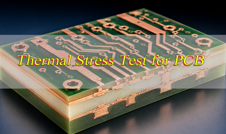
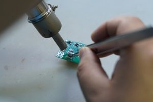
A ceramic PCB prototype is a small-batch ceramic circuit board built to verify thermal performance, electrical stability, solderability, manufacturability, and application fit before moving into volume production. Unlike standard FR4 prototypes, ceramic boards use inorganic substrates such as alumina, aluminum nitride, or silicon nitride, and they are often selected for high-power LEDs, power modules, sensors, RF modules, medical electronics, EV electronics, aerospace systems, and other demanding applications.
What Is a Ceramic PCB Prototype?
A ceramic PCB prototype is an early production sample of a circuit board made with a ceramic substrate instead of a glass-fiber epoxy laminate. The substrate may be alumina, aluminum nitride, silicon nitride, or another ceramic material, depending on the thermal, mechanical, dielectric, and reliability requirements of the project.
In most projects, the prototype is used to check several key points:
| Prototype Purpose | What It Helps Verify |
|---|---|
| Electrical performance | Continuity, insulation, impedance-related behavior, conductor quality |
| Thermal performance | Heat spreading, junction temperature reduction, thermal path efficiency |
| Mechanical fit | Board size, hole position, mounting tolerance, substrate thickness |
| Assembly readiness | Solderability, component placement, paste behavior, reflow compatibility |
| Reliability risk | Cracking, delamination, copper adhesion, thermal cycling behavior |
| Cost feasibility | Material cost, process cost, yield expectation, volume production price |
A ceramic PCB prototype is especially useful when the final product must operate under high temperature, high current density, fast heat transfer, or long service-life conditions.
Why Ceramic PCB Prototype Is Important Before Mass Production?
Ceramic boards are more expensive and process-sensitive than common FR4 boards. A small design or material mismatch can create higher scrap cost during mass production. Prototyping helps detect these issues early.
For example, an LED module may look correct in the Gerber file but still show poor heat dissipation if the copper area is too small or the ceramic material is not suitable. A power module may pass electrical continuity testing but fail later if copper thickness, bonding method, and thermal cycling requirements are not aligned. A sensor substrate may need tighter dimensional control because even a small deviation can affect package alignment.
Prototype validation gives the engineering and purchasing teams a safer path. It allows them to confirm the design window, test assembly behavior, compare materials, review DFM feedback, and decide whether the board is ready for batch production.
How Does a Ceramic PCB Prototype Work?
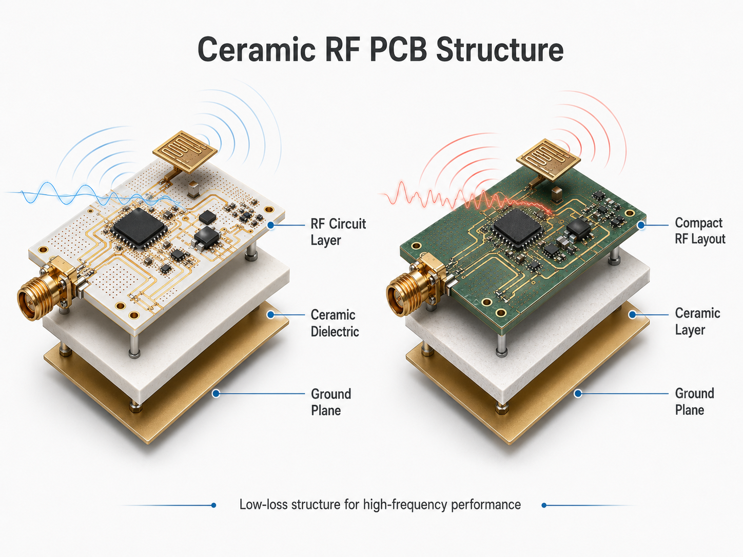
A ceramic PCB works by combining electrical routing with a thermally stable ceramic base. The copper or conductive layer transfers signals and current, while the ceramic substrate provides insulation, heat spreading, and dimensional stability.
The working logic is simple:
| Layer or Feature | Main Function |
|---|---|
| Copper circuit layer | Carries current and signal |
| Ceramic substrate | Provides insulation and thermal transfer |
| Surface finish | Protects copper and supports soldering or bonding |
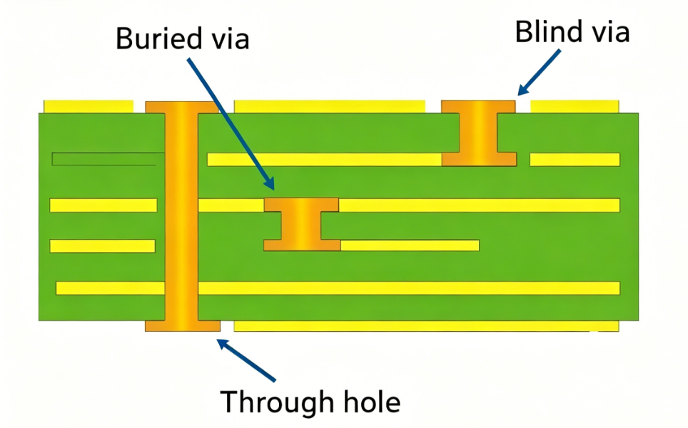
| Via or metallized hole | Creates electrical connection between layers or sides |
| Solder mask or protective coating | Used when required for insulation and surface protection |
| Mounting interface | Transfers heat to heatsink, housing, or metal base |
The material and process decide how well the prototype performs. Alumina is widely used because it offers a balanced cost-performance profile. Aluminum nitride is chosen when stronger thermal conductivity is needed. Silicon nitride can be considered for applications that need stronger mechanical toughness.
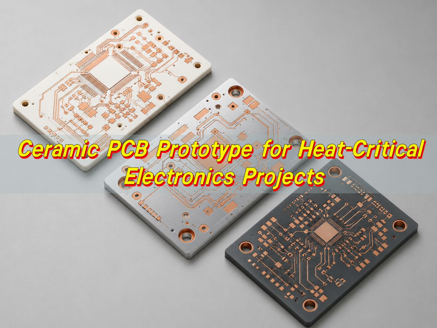
Main Types of Ceramic PCB Prototype
Ceramic PCB prototypes can be classified by substrate material, conductor formation process, layer structure, and application requirement.
| Type | Common Use | Main Advantage |
|---|---|---|
| Alumina Ceramic PCB Prototype | LED, sensors, power control, industrial modules | Stable cost and mature process |
| Aluminum Nitride Ceramic PCB Prototype | High-power LED, laser, power module, RF power device | Higher thermal conductivity |
| Silicon Nitride Ceramic PCB Prototype | Power electronics, automotive, harsh environments | Better mechanical toughness |
| Thick Film Ceramic PCB Prototype | Sensors, hybrid circuits, resistive circuits | Suitable for printed conductor patterns |
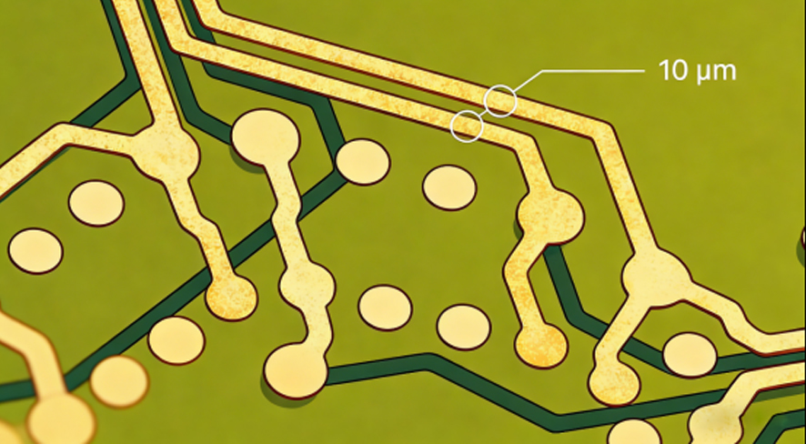
| Thin Film Ceramic PCB Prototype | RF, microwave, precision circuits | Fine lines and high accuracy |
| DPC Ceramic PCB Prototype | Fine circuit, LED, medical, power modules | Good line precision and copper plating control |
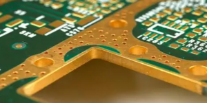
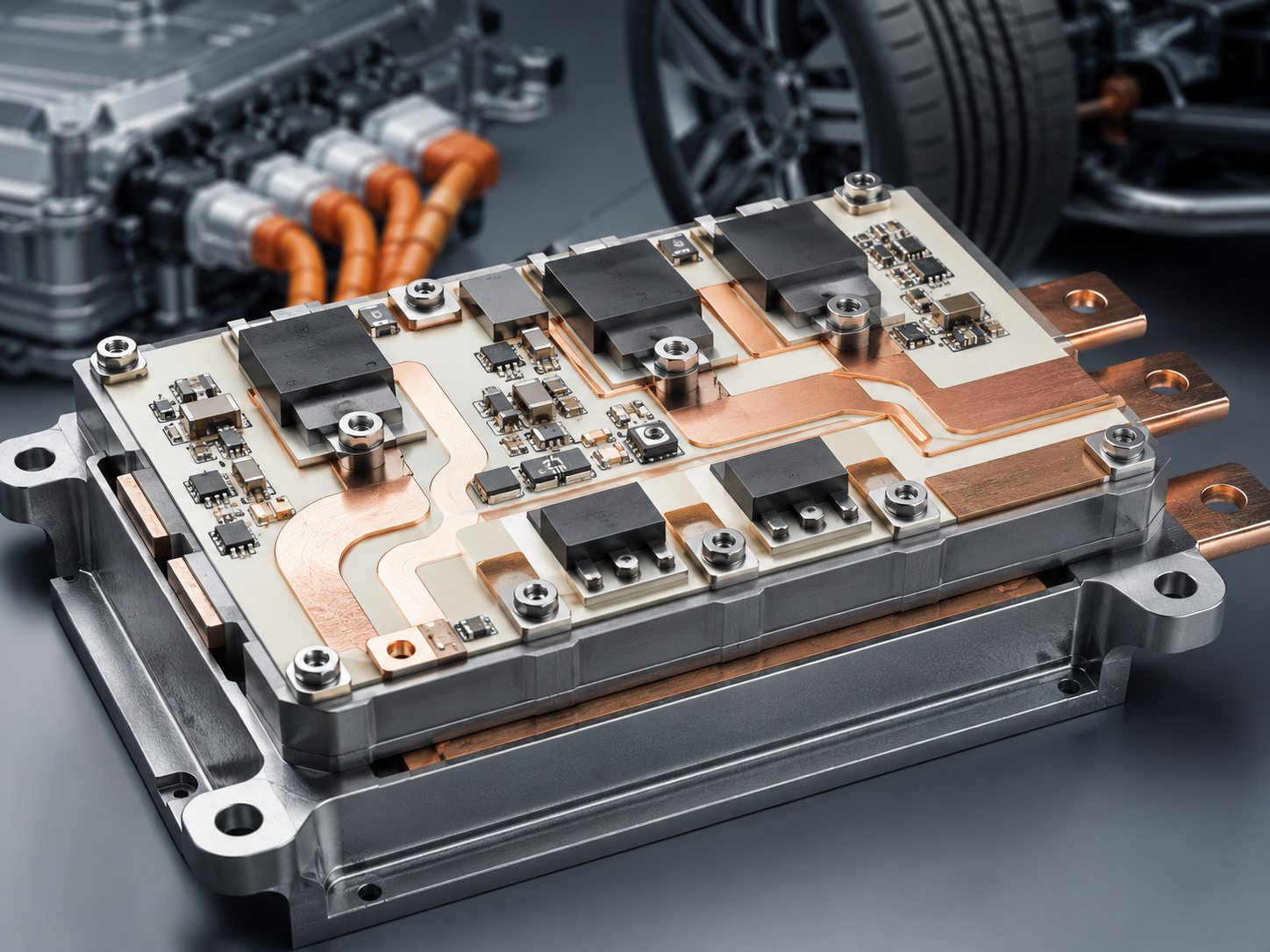
| DBC Ceramic PCB Prototype | Power modules, IGBT, high-current circuits | Thick copper and strong current capacity |
| AMB Ceramic Substrate Prototype | EV power modules, high-reliability power systems | Strong bonding for demanding thermal cycling |
DPC, DBC, and AMB are common ceramic circuit manufacturing routes. Each process has its own cost, copper thickness range, line capability, and reliability profile.
Which Materials Are Used for Ceramic PCB Prototype?
Material selection is one of the most important decisions in ceramic PCB prototyping. The material affects thermal conductivity, dielectric strength, coefficient of thermal expansion, machinability, cost, and long-term reliability.
| Material | Typical Selection Reason | Common Applications |
|---|---|---|
| Alumina, Al₂O₃ | Balanced cost, good insulation, mature supply | LED modules, sensors, industrial electronics |
| Aluminum Nitride, AlN | High thermal conductivity, good insulation | High-power LED, power modules, laser electronics |
| Silicon Nitride, Si₃N₄ | Stronger mechanical toughness | EV power electronics, harsh thermal cycling applications |
| LTCC Ceramic | Multilayer ceramic integration | RF modules, filters, compact high-frequency circuits |
| BeO | High thermal performance but limited use due to handling concerns | Legacy or specialized thermal applications |
For most early-stage prototypes, alumina is the practical starting point when the project needs ceramic stability without extreme thermal requirements. AlN becomes more suitable when heat dissipation is a core performance target. Silicon nitride is more specialized and is usually selected when thermal cycling and mechanical robustness are both important.
Key Features of Ceramic PCB Prototype
Ceramic PCB prototypes are selected because they provide performance characteristics that organic laminates cannot always offer.
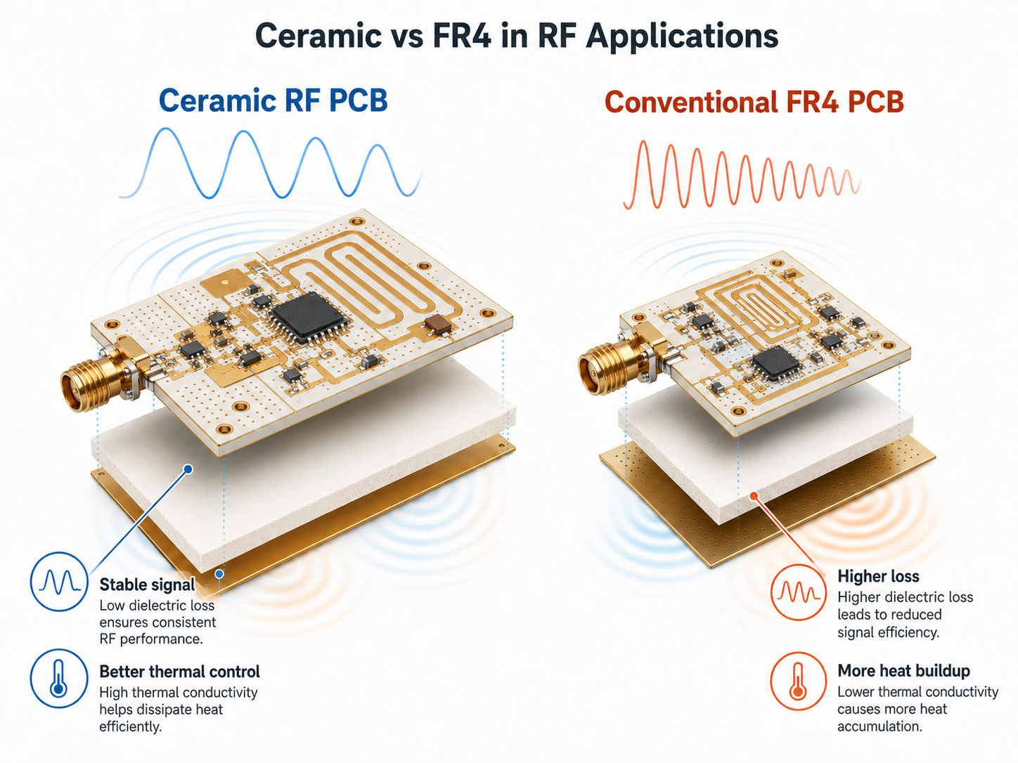
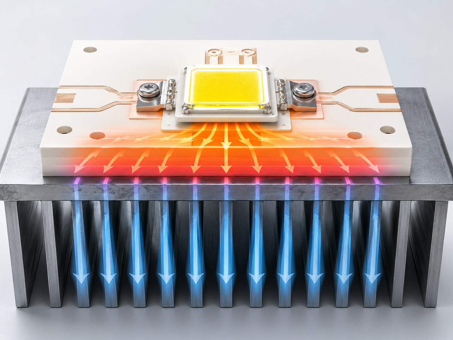
High Thermal Conductivity
Ceramic materials can move heat away from components more efficiently than standard FR4. This is useful for LEDs, power semiconductors, laser diodes, and compact power modules.
Strong Electrical Insulation
Ceramic substrates offer good dielectric behavior, making them suitable for circuits that require insulation between conductive paths and heat-dissipation structures.
Low Thermal Expansion Mismatch
The coefficient of thermal expansion of some ceramic materials can better match semiconductor packages, helping reduce stress during heating and cooling cycles.
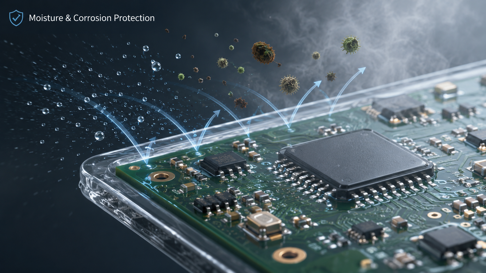
Stable Performance in Harsh Conditions
Ceramic substrates are inorganic, rigid, and dimensionally stable. They are often used when long-term stability matters more than the lowest board cost.
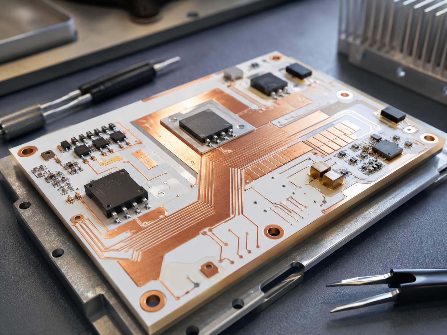
Good Compatibility with High-Power Designs
DBC and AMB ceramic substrates can support thick copper structures for high-current and power module applications.
Advantages and Limitations of Ceramic PCB Prototype
A ceramic PCB prototype offers strong technical value, but it should be selected for the right reason. It is not a universal replacement for FR4, aluminum PCB, or copper substrate PCB.
| Aspect | Advantage | Limitation |
|---|---|---|
| Thermal performance | Strong heat transfer and temperature stability | Higher material and process cost |
| Electrical insulation | Good dielectric properties | Material choice must match voltage and frequency |
| Mechanical stability | Rigid and dimensionally stable | Ceramic is brittle and needs careful handling |
| Reliability | Suitable for demanding applications | Requires proper copper bonding and thermal cycling review |
| Assembly | Can support SMT and selected through-hole needs | Reflow profile and mounting stress must be controlled |
| Prototyping | Helps verify performance before mass production | Lead time is usually longer than standard FR4 prototypes |
The main decision is practical: use ceramic when the product needs thermal, electrical, or reliability performance that a standard PCB structure cannot provide economically or safely.
Ceramic PCB Prototype vs FR4 PCB, Aluminum PCB, and Copper Substrate PCB
Many buyers compare ceramic PCB with FR4, aluminum PCB, and copper substrate PCB before prototyping. The right choice depends on heat density, insulation requirement, circuit complexity, cost target, and product lifetime.
| Board Type | Best Fit | Thermal Performance | Cost Level | Notes |
|---|---|---|---|---|
| FR4 PCB | General electronics, control boards, digital circuits | Low to medium | Low | Best for standard circuits |
| High-Tg FR4 PCB | Higher soldering temperature, industrial boards | Medium | Low to medium | Good for improved thermal resistance, not strong heat spreading |
| Aluminum PCB | LED lighting, moderate power electronics | Medium to high | Medium | Good cost-performance for many LED products |
| Copper Substrate PCB | High-power LED, power conversion | High | Medium to high | Strong heat spreading, heavier structure |
| Ceramic PCB | High-power, high-temperature, RF, medical, aerospace, EV modules | High to very high | High | Best when heat, insulation, and stability matter together |
FR4 remains the first option for many electronic products. Aluminum PCB is often better for cost-controlled LED and heat-dissipation projects. Ceramic PCB is more suitable when the product needs higher thermal conductivity, better dimensional stability, or stronger reliability under demanding operating conditions.
How to Choose the Right Ceramic PCB Prototype?
Choosing the right ceramic PCB prototype starts with the application requirement, not the material name.
Before selecting a ceramic substrate, engineers should define:
| Selection Factor | Recommended Review |
|---|---|
| Power density | Heat source size, wattage, thermal path |
| Operating temperature | Continuous temperature and peak temperature |
| Circuit precision | Minimum line width, spacing, via requirement |
| Copper thickness | Current capacity and thermal spreading need |
| Surface finish | Soldering, wire bonding, corrosion resistance |
| Assembly method | SMT, through-hole, wire bonding, die attach |
| Reliability target | Thermal cycling, vibration, humidity, service life |
| Cost target | Prototype budget and volume production estimate |
For an LED module, the most important points may be heat dissipation, solderability, and mounting flatness. For a power module, copper thickness, bonding strength, and thermal cycling matter more. For RF or microwave circuits, dimensional precision, dielectric stability, and surface finish become more important.
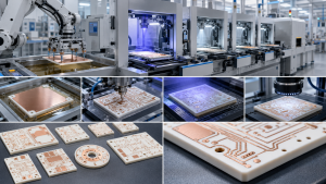
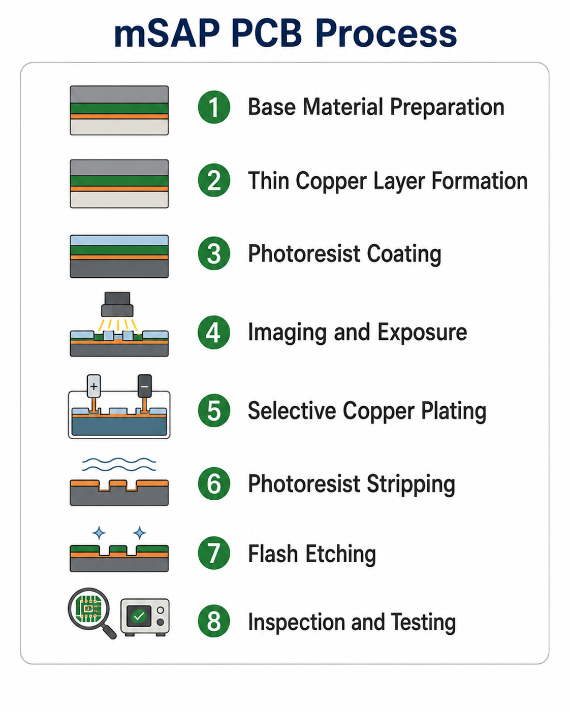
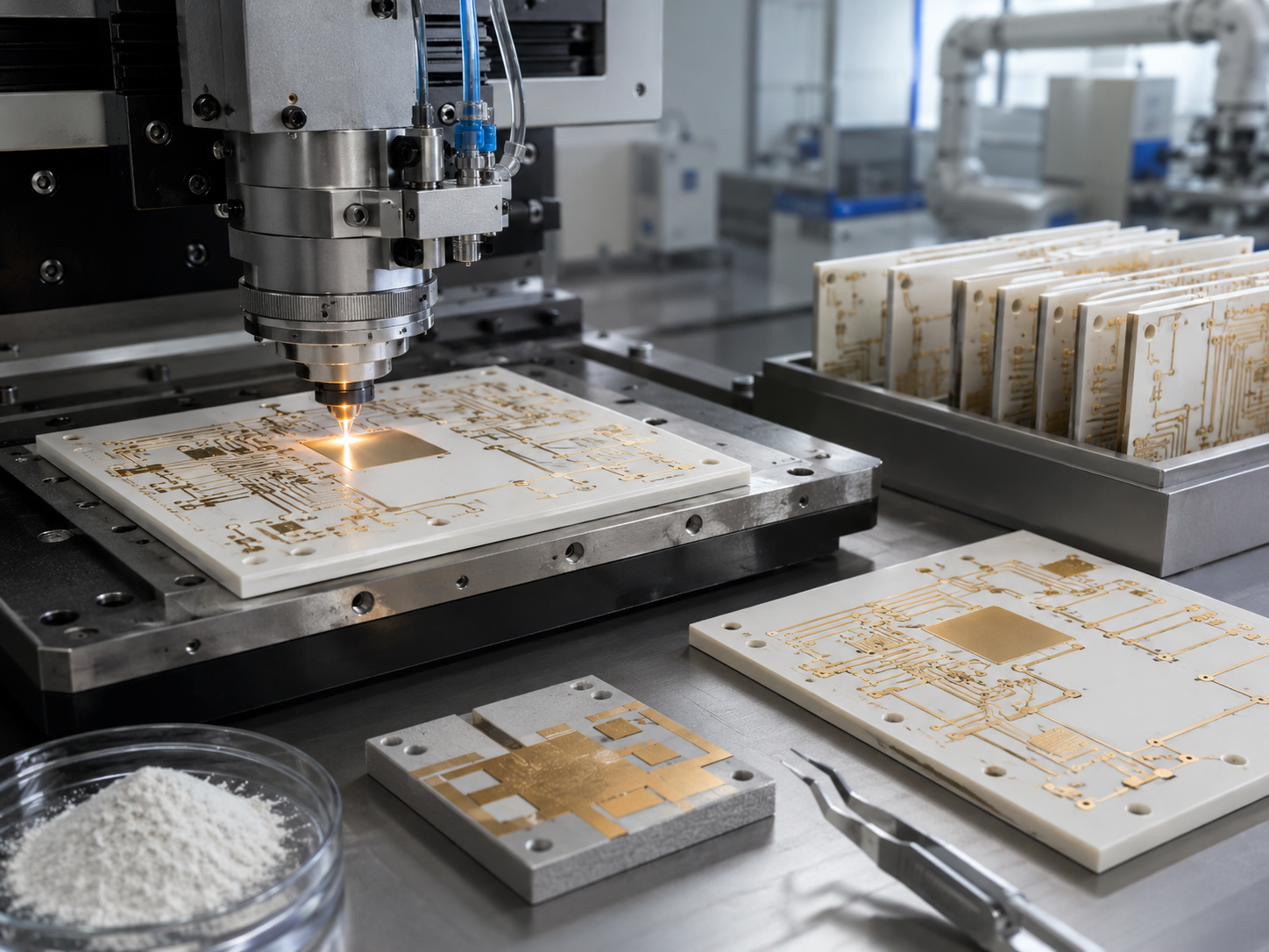
Manufacturing Process for Ceramic PCB Prototype
Ceramic PCB prototyping usually starts with engineering file review and material confirmation. After that, the process depends on the selected technology.
A typical flow may include:
| Step | Purpose |
|---|---|
| File review and DFM check | Confirm Gerber, drill, copper, tolerance, finish, and manufacturability |
| Material preparation | Select alumina, AlN, Si₃N₄, or other ceramic substrate |
| Laser cutting or drilling | Form board outline, holes, slots, or cavities |
| Metallization or copper bonding | Create conductive layer through DPC, DBC, AMB, thick film, or thin film process |
| Pattern formation | Define circuit traces, pads, and copper areas |
| Surface finish | Apply ENIG, ENEPIG, silver, gold, or other required finish |
| Inspection and testing | Check dimensions, circuit quality, insulation, adhesion, and appearance |
| Packaging | Protect brittle ceramic boards during shipment |
The prototype stage should include DFM feedback before production. This helps identify issues such as narrow copper bridges, unsuitable hole-to-edge distance, excessive panel stress, large unsupported ceramic areas, or surface finish mismatch.
Testing Methods and Quality Standards for Ceramic PCB Prototype
Ceramic PCB prototypes should not rely only on visual inspection. Testing depends on product use, but common controls include electrical testing, dimensional inspection, appearance inspection, copper adhesion review, solderability testing, and thermal-related checks.
| Test or Inspection | Why It Matters |
|---|---|
| Electrical test | Confirms open/short condition |
| AOI | Checks pattern quality and visible defects |
| Dimensional inspection | Confirms outline, hole, slot, and tolerance |
| Surface finish inspection | Checks soldering or bonding readiness |
| Adhesion testing | Reviews copper-to-ceramic bonding quality |
| Thermal shock or cycling | Evaluates stress under heating and cooling |
| X-ray inspection | Useful for assembly, hidden solder joints, or void review |
| Cross-section analysis | Checks metallization, vias, and internal structure when required |
For quality references, IPC-6012F covers qualification and performance requirements for rigid printed boards, including conductor, hole, plating, acceptance testing, and electrical, mechanical, and environmental requirements. IPC-A-600 provides visual acceptability criteria for printed boards, while IPC-J-STD-001 addresses requirements for soldered electrical and electronic assemblies.
For European-market electronics, RoHS compliance is also commonly reviewed because it restricts hazardous substances in electrical and electronic equipment.
Common Failure Problems in Ceramic PCB Prototype
A prototype is valuable because it exposes problems before they become expensive production failures.
| Problem | Possible Cause | Practical Solution |
|---|---|---|
| Ceramic cracking | Board stress, poor mounting design, rough handling | Optimize mounting holes, edge clearance, packaging, and assembly fixtures |
| Copper peeling | Weak bonding, unsuitable process, thermal stress | Review DPC/DBC/AMB choice, copper thickness, and adhesion requirement |
| Poor solder wetting | Wrong surface finish, storage issue, contaminated surface | Confirm finish type, shelf life, cleaning, and soldering profile |
| Warpage or flatness issue | Substrate thickness, copper imbalance, process stress | Balance copper distribution and review substrate thickness |
| Hot spot remains high | Insufficient copper area or wrong material | Increase thermal copper, use AlN, improve heatsink interface |
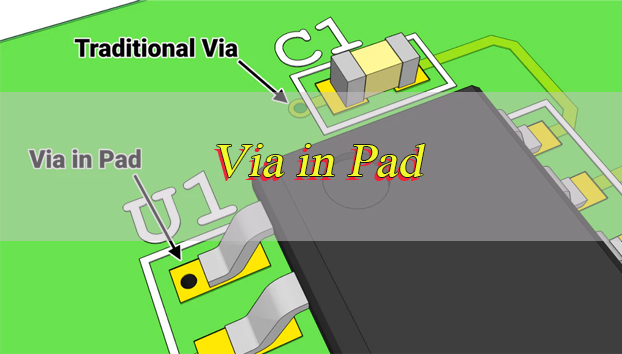
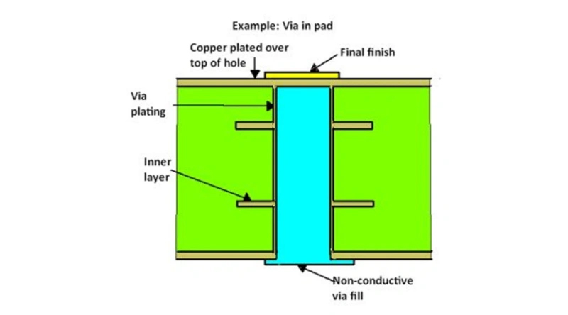
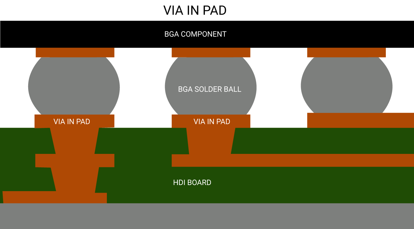
| Via reliability issue | Unsuitable via structure or metallization | Confirm via diameter, filling, plating, and reliability test |
| Chipping at edges | Cutting stress or packaging impact | Improve laser cutting, edge clearance, and protective packing |
| Assembly fracture | Excessive pressure, fixture stress, screw torque | Control mounting torque and use suitable support fixtures |
Many ceramic PCB failures come from mechanical stress rather than electrical design. The board is strong under the right conditions, but brittle when point stress, bending, or uneven mounting force is introduced.
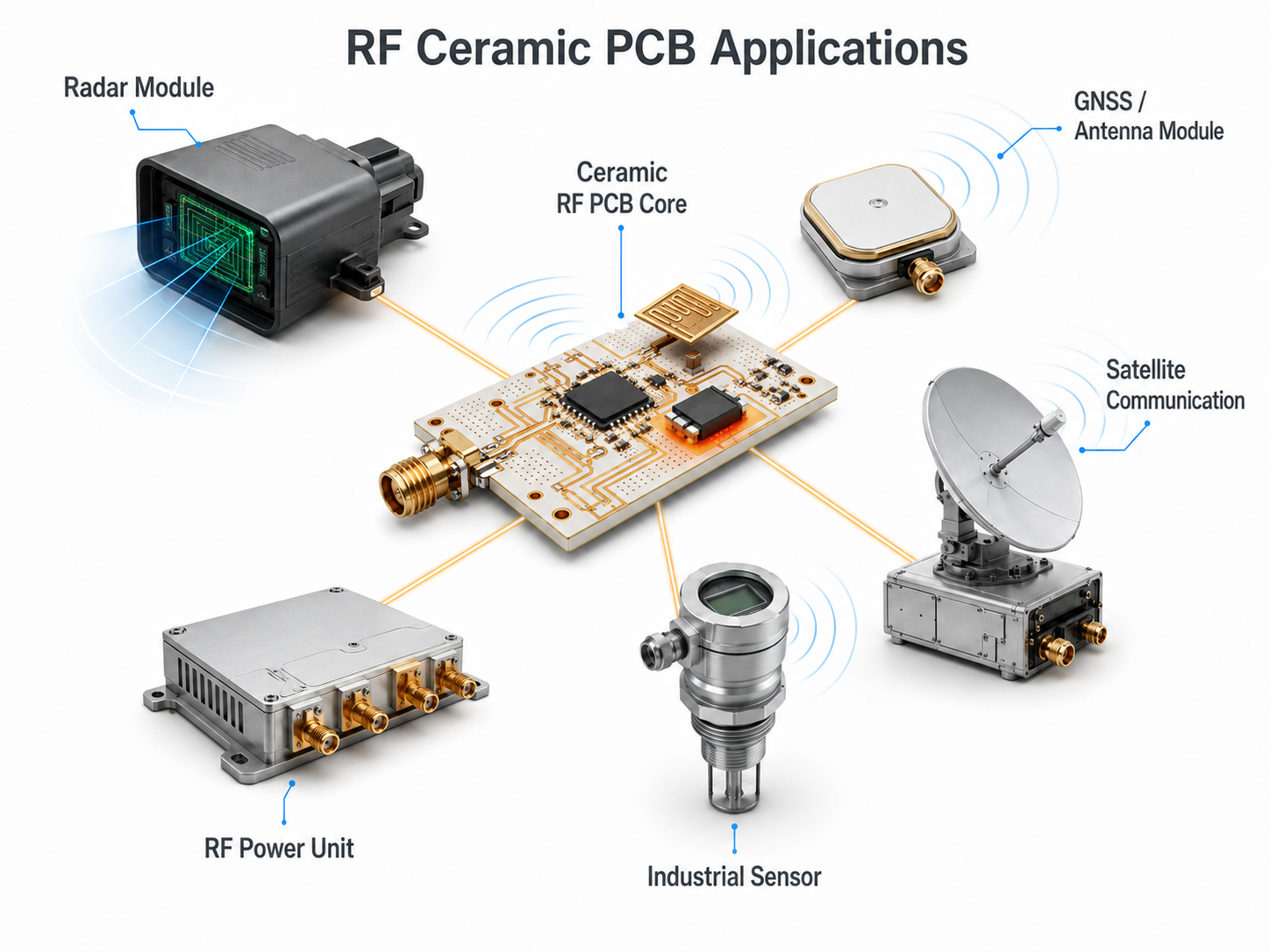
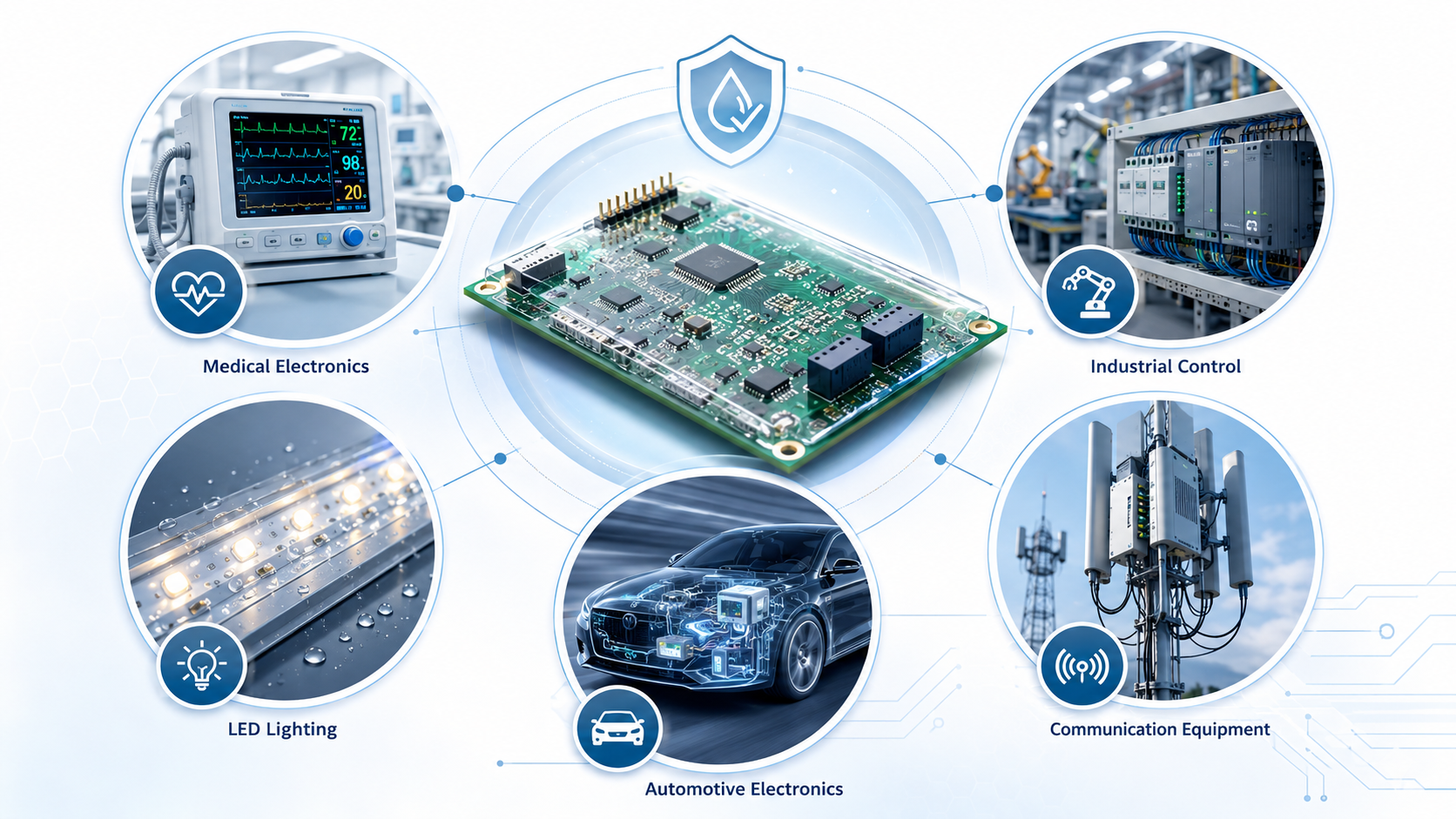
Ceramic PCB Prototype Applications by Industry
Ceramic PCB prototypes are used in industries where heat, insulation, dimensional stability, and reliability are important.
| Industry | Typical Use |
|---|---|
| LED Lighting | High-power LEDs, UV LEDs, COB modules, automotive lighting |
| Power Electronics | IGBT modules, MOSFET modules, converters, inverters |
| Automotive Electronics | EV power modules, battery systems, headlights, sensors |
| Medical Electronics | Diagnostic equipment, imaging modules, sensor circuits |
| Aerospace and UAV | High-reliability control modules, RF modules, power circuits |
| Telecommunications | RF power devices, microwave modules, antenna-related circuits |
| Industrial Control | Motor drives, high-temperature sensors, automation modules |
| New Energy | Solar inverter modules, energy storage systems, charging electronics |
For example, an aluminum nitride ceramic PCB prototype may be selected for a compact high-power LED module because heat must move away from the LED junction quickly. An alumina ceramic PCB prototype may be used for a sensor module where insulation, stability, and cost balance are more important than extreme heat transfer.
Practical Case Examples for Ceramic PCB Prototype
Case 1: High-Power LED Module
A customer developing a high-brightness LED module needs better thermal transfer than FR4 can provide. The prototype uses alumina or AlN ceramic with optimized copper pads and a controlled surface finish. During validation, the team checks solder wetting, junction temperature, optical stability, and mounting flatness. If the temperature remains too high, the design may move from alumina to AlN or increase the copper heat-spreading area.
Case 2: Power Semiconductor Substrate
A power module project needs thick copper, strong bonding, and stable thermal cycling behavior. DBC or AMB ceramic substrate may be reviewed. The prototype helps verify copper adhesion, isolation, current path, and package compatibility. In this type of project, copper structure and thermal cycling performance are usually more important than low prototype cost.
Case 3: Precision Sensor Circuit
A sensor module requires stable insulation and accurate conductor geometry. Alumina ceramic may be enough if the thermal load is moderate. The prototype focuses on dimensional tolerance, surface finish, assembly process, and signal stability. Early DFM review helps prevent fragile edges, narrow spacing risks, and poor solder-pad design.
Cost Factors for Ceramic PCB Prototype
Ceramic PCB prototype cost is affected by material, size, thickness, copper structure, process technology, surface finish, tolerance, testing requirement, and quantity.
| Cost Factor | Cost Impact |
|---|---|
| Material type | AlN and Si₃N₄ usually cost more than alumina |
| Board size | Larger ceramic panels increase material cost and breakage risk |
| Substrate thickness | Special thickness may require custom material preparation |
| Copper thickness | Thicker copper increases process complexity |
| Process type | AMB, DBC, DPC, thick film, and thin film have different cost levels |
| Line width and spacing | Fine circuits require tighter process control |
| Surface finish | ENIG, ENEPIG, silver, gold, or wire-bondable finish affects cost |
| Testing level | Extra reliability testing increases validation cost |
| Quantity | Small batches carry higher unit setup cost |
A low prototype price is not always the best purchasing target. For ceramic PCB projects, the better question is: does the prototype process match the final production method? If the prototype uses a shortcut that cannot scale, the sample may pass testing but still fail during mass production transfer.
Global Procurement Considerations for Ceramic PCB Prototype
Global buyers usually care about technical accuracy, documentation, lead time, export stability, and communication speed. A China-based source factory can support international customers without claiming overseas factories, warehouses, or local branches.
For customers in North America and Europe, common concerns include quality traceability, RoHS compliance, IPC-related documentation, stable surface finish, and long-term repeatability. For Southeast Asia and other cost-sensitive markets, buyers often care more about small-batch flexibility, competitive pricing, practical lead time, and stable export logistics.
A reliable supplier should help buyers confirm:
| Procurement Question | Why It Matters |
|---|---|
| Is the material clearly specified? | Avoids wrong substrate substitution |
| Is the prototype process suitable for mass production? | Reduces transfer risk |
| Are tolerances realistic? | Prevents yield loss and rework |
| Is the surface finish matched to assembly? | Improves soldering or bonding quality |
| Are test reports available when needed? | Supports engineering approval |
| Can the supplier support batch production after prototype approval? | Saves time after validation |
| Are packaging and shipping suitable for brittle ceramic boards? | Reduces transit damage |
Good procurement is not only about finding a ceramic PCB prototype supplier. It is about finding a supplier that understands thermal design, ceramic brittleness, copper bonding, surface finish, assembly behavior, and production consistency.
How to Choose a Ceramic PCB Prototype Supplier?
A ceramic PCB prototype supplier should be evaluated by engineering capability, process matching, inspection control, communication quality, and production scalability.
| Supplier Capability | What to Check |
|---|---|
| Ceramic material experience | Alumina, AlN, Si₃N₄, DBC, DPC, AMB, thick film, thin film |
| DFM support | Ability to review manufacturability before production |
| Process transparency | Clear explanation of material, finish, tolerance, and test plan |
| Quality control | AOI, electrical test, dimensional inspection, adhesion review |
| Assembly understanding | Knowledge of soldering, wire bonding, die attach, thermal interface |
| Documentation | Material confirmation, inspection report, RoHS support when required |
| Production transfer | Ability to move from prototype to small batch and mass production |
| Export experience | Safe packaging, global shipping, responsive technical communication |
The right supplier should not simply accept every file without review. For ceramic boards, a careful supplier will ask about application environment, thermal load, copper thickness, soldering method, surface finish, tolerance, and expected production quantity.
What Files Are Needed Before Ordering a Ceramic PCB Prototype?
Clear files reduce engineering back-and-forth and improve prototype accuracy.
| File or Information | Required Details |
|---|---|
| Gerber files | Copper layers, outline, solder mask, paste, legend if needed |
| Drill file | Hole size, plated/non-plated hole definition |
| Stack-up or structure drawing | Material, thickness, copper thickness, layer requirement |
| Surface finish requirement | ENIG, ENEPIG, silver, gold, OSP if applicable |
| Material requirement | Alumina, AlN, Si₃N₄, DBC, DPC, AMB, or other |
| Quantity | Prototype quantity and possible batch quantity |
| Tolerance requirement | Board size, hole, slot, thickness, flatness |
| Assembly requirement | SMT, through-hole, wire bonding, die attach |
| Test requirement | Electrical test, thermal test, inspection report, reliability test |
| Application background | LED, power module, RF, sensor, medical, automotive, aerospace |
If the project is still in early development, the buyer can provide available files first and request a DFM review. However, PCB design responsibility should remain with the customer or their design team. A manufacturer can review manufacturability, suggest layout-related improvements, and support production feasibility, but it should not replace the customer’s circuit design responsibility.
FAQ About Ceramic PCB Prototype
What is a ceramic PCB prototype used for?
A ceramic PCB prototype is used to verify whether a ceramic circuit board can meet electrical, thermal, mechanical, and assembly requirements before mass production. It helps engineers test material choice, copper layout, surface finish, solderability, dimensional tolerance, and heat dissipation performance in a controlled small-batch stage.
Is ceramic PCB better than FR4 PCB?
Ceramic PCB is better than FR4 when the project needs higher thermal conductivity, stronger temperature stability, or better insulation under demanding conditions. FR4 is still better for many standard control boards, digital circuits, and cost-sensitive products. The right choice depends on the application, not only on material performance.
Which ceramic material is best for PCB prototype?
Alumina is often selected for balanced cost and stable performance. Aluminum nitride is better for high-power heat dissipation. Silicon nitride is suitable when mechanical toughness and thermal cycling resistance are important. The best material depends on power density, temperature, insulation, reliability, and budget.
How long does a ceramic PCB prototype take?
Lead time depends on material, process, copper thickness, surface finish, tolerance, and testing requirement. Simple alumina prototypes may be faster, while AlN, DBC, AMB, multilayer ceramic, or high-reliability prototypes usually need more engineering and process time. The timeline should start after DFM and material confirmation.
Can ceramic PCB prototypes support SMT assembly?
Yes. Ceramic PCB prototypes can support SMT assembly when pad design, surface finish, solder paste, reflow profile, and component layout are correctly controlled. Because ceramic is rigid and brittle, fixture design, mounting pressure, and thermal stress should be reviewed before assembly.
Can ceramic PCB prototypes use through-hole components?
Through-hole components can be used in some ceramic PCB designs, but hole metallization, ceramic thickness, mechanical stress, and soldering process must be reviewed carefully. SMT is more common for many ceramic substrate applications, while through-hole use requires stronger manufacturability confirmation.
Why is ceramic PCB prototype more expensive?
Ceramic PCB prototypes cost more because ceramic substrates, copper bonding, laser processing, metallization, surface finishing, and inspection are more specialized than standard FR4 processing. Small quantities also carry setup cost. However, prototyping can reduce larger losses by preventing wrong material or process decisions.
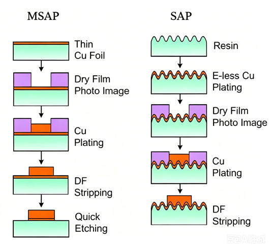
What is the difference between DPC and DBC ceramic PCB?
DPC ceramic PCB uses direct plated copper and is often selected for finer circuits and controlled copper formation. DBC ceramic PCB bonds copper directly to ceramic and is often used for power modules requiring thicker copper. The better choice depends on line precision, current load, thermal demand, and cost target.
Is aluminum nitride ceramic PCB worth the cost?
Aluminum nitride is worth considering when heat dissipation is a core performance requirement. If alumina cannot reduce operating temperature enough, AlN may improve thermal transfer. For moderate thermal loads, alumina may provide a better cost-performance balance.
What surface finish is used on ceramic PCB prototypes?
Common surface finishes include ENIG, ENEPIG, silver, gold, and other application-specific finishes. The choice depends on soldering, wire bonding, storage life, corrosion risk, and assembly process. Wire bonding applications need special attention to finish type and bonding compatibility.
What causes ceramic PCB cracking?
Cracking is often caused by mechanical stress, poor mounting design, excessive screw torque, rough handling, edge impact, or thermal shock. Proper board thickness, hole clearance, edge design, fixture support, packaging, and assembly process control can reduce this risk.
Can ceramic PCB prototypes be used for high-frequency circuits?
Yes, ceramic substrates can be used in high-frequency and microwave applications when dielectric properties, conductor precision, surface finish, and layout requirements are properly controlled. Thin film ceramic processes are often considered when fine lines and high precision are required.
What should buyers confirm before placing a ceramic PCB prototype order?
Buyers should confirm material, thickness, copper thickness, surface finish, tolerance, test requirements, application environment, assembly method, quantity, and target production volume. Clear information allows the supplier to give accurate DFM feedback and avoid wrong process selection.
Can a ceramic PCB prototype move directly to mass production?
It can move to mass production if the prototype process, material, supplier capability, and inspection criteria match the planned production method. Before scaling, the buyer should review test results, assembly yield, thermal data, dimensional accuracy, and any DFM changes.
How do I choose a ceramic PCB prototype manufacturer?
Choose a manufacturer with real ceramic PCB process experience, DFM support, material knowledge, inspection capability, export experience, and batch production capacity. A good supplier should understand ceramic brittleness, copper bonding, solderability, thermal management, and quality documentation.
Conclusion:
A ceramic PCB prototype is a practical engineering step for products that need stronger heat dissipation, stable insulation, high-temperature performance, or long-term reliability.
If your project requires a ceramic PCB prototype for high-power LED modules, power electronics, sensors, RF devices, medical electronics, automotive systems, aerospace modules, or industrial control products, our engineering team can support material selection, DFM review, prototype fabrication, small-batch production, and volume manufacturing.
Send us your Gerber files, stack-up requirements, drawings, BOM, or application details, and we will help review the technical feasibility and provide a reliable quotation. For ceramic PCB prototype, OEM manufacturing, sample development, batch production, or custom engineering support, please contact us at sales@bestpcbs.com