PCB manufacturing PCB manufacturing
Home > Blog

DCB ceramic pcb

Alumina Substrate Manufacturer for Custom Ceramic PCBs
Thursday, September 3rd, 2026

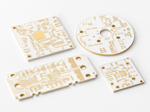
At EBest Circuit (Best Technology), we manufacture custom ceramic PCBs using an alumina substrate as the electrically insulating base. We turn an alumina ceramic substrate into a patterned circuit through thick-film, thin-film or copper-metallization processes. Our manufacturing support covers substrate selection, circuit fabrication and agreed assembly work for hybrid electronics, LED modules and power circuits.
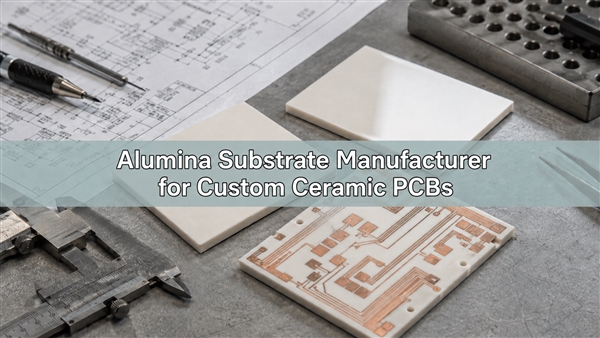
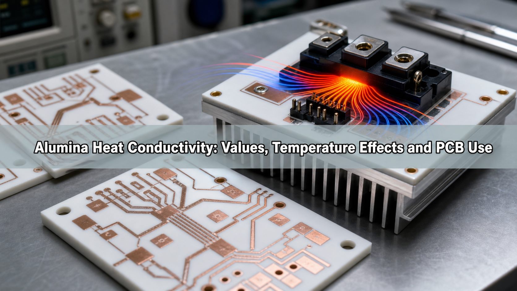
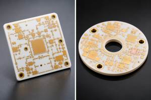
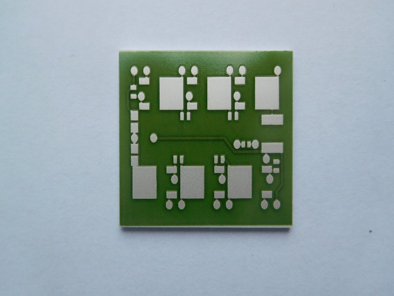
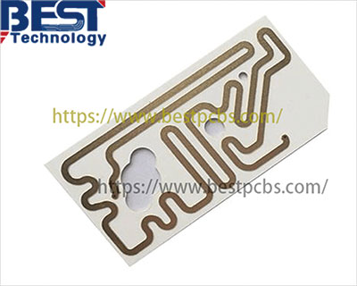
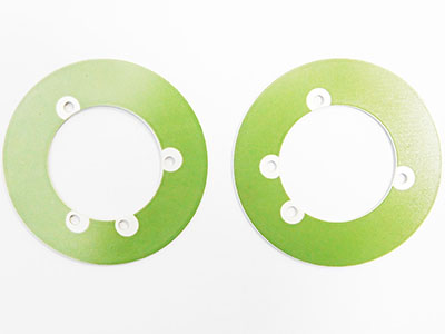
Alumina substrate manufacturer for custom ceramic PCBs with bare and metallized ceramic samples

What Is an Alumina Substrate?

Alumina is aluminum oxide, or Al2O3. A ceramic alumina substrate is a formed and fired plate used as the foundation of an electronic circuit. A bare alumina plate has no conductive pattern; an alumina PCB adds patterned metallization and may include printed resistors, additional dielectric layers and assembled components.

Why is alumina a good substrate? It combines electrical insulation, useful heat conduction, dimensional stability and compatibility with several circuit-forming processes. It is usually opaque white or ivory, not transparent glass. An alumina ceramic insulator also remains mechanically brittle: strong support in service does not make a thin tile resistant to bending or edge impact.

Which Alumina Substrate Properties Matter for Ceramic PCBs?

The physical properties of alumina determine insulation, heat transfer and handling limits. Alumina structure, including grains and pores, changes these results even at similar purity. This alumina property table summarizes representative commercial 96–99.6% electronic-substrate grades, not our finished-board acceptance limits. Use the selected alumina substrate datasheet to confirm alumina material properties for your design.

Property Representative value and condition Practical significance
Alumina thermal conductivity 20–29 W/m·K at 25°C Heat conduction through the ceramic
Alumina substrate dielectric constant / relative permittivity 9.8–9.9 at 1 MHz Al2O3 dielectric constant affects capacitance and impedance
Alumina substrate loss tangent 0.0002 at 1 MHz for the listed electrical grades Dielectric loss; not a microwave-frequency guarantee
Alumina resistivity Volume resistivity >1014 Ω·cm at 25°C Limits leakage through the ceramic body
Dielectric breakdown strength >15 kV/mm, DC material test Insulation reference, not a finished-board working-voltage rating
Alumina substrate CTE 6.7–6.8 ppm/K over 40–400°C Alumina CTE affects stress at bonded interfaces
Density 3.60–3.90 g/cm³ Mass and grade consistency
Specific heat capacity of alumina 750–780 J/kg·K at 25°C Energy absorbed during temperature changes
Flexural strength 370–500 MPa, three-point bending One measure of alumina mechanical properties under bending
Young’s modulus of alumina 330 GPa for the listed tested grades Elastic stiffness, not fracture strength
Vickers hardness 14–16 GPa for the listed tested grades Wear resistance and machining difficulty
Surface roughness, Ra 0.1–0.4 μm across the listed grades Surface suitability for deposited circuit features
Chemical properties of alumina Resistant to many oils and chemicals; compatibility depends on exposure Cleaning must also suit the metal, resistors and coatings

Alumina strength depends on loading: alumina compressive strength and tensile strength of alumina are not interchangeable with the bending values above. For a brittle alumina board, fracture and edge quality matter more than a metal-style yield strength of alumina specification.

How Do 96% and 99.6% Alumina Substrates Differ?

A 96% alumina substrate is widely associated with thick-film circuits. Its surface and glass-phase chemistry must be compatible with the selected conductor and resistor pastes. A 99.6% alumina substrate is commonly considered for fine thin-film patterns where surface quality and processing consistency are important. Higher purity does not, by itself, guarantee higher thermal conductivity or lower finished-board cost.
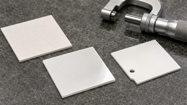
Conceptual comparison of matte and polished alumina substrate surfaces and ceramic thickness

A fine polished alumina substrate can reduce surface irregularities that interfere with fine features. However, polishing is an additional process, not an automatic consequence of selecting a purity. Specify roughness, flatness and acceptable defects separately from composition. Dense alumina is generally appropriate for circuit substrates; alumina porosity must be controlled rather than selected to imitate porous filter ceramics.

For high-purity alumina ceramic substrate development, we match surface finish and metal adhesion to the circuit process. A high purity alumina substrate still needs grade-specific acceptance criteria. A porous alumina substrate is a separate structure, so the dense-grade values above do not apply to it.

How Does Alumina Heat Conductivity Change with Temperature?

Alumina substrate thermal conductivity generally decreases as temperature rises over the operating range relevant to many electronic modules. Use a grade-specific temperature curve, not a straight line invented from a room-temperature value. Al2O3 thermal conductivity also describes the ceramic material, not the thermal resistance of the complete mounted board.

For a simple one-dimensional estimate, ceramic thermal resistance is R = t/(k × A), where t is thickness, k is thermal conductivity and A is the heat-flow area. At an assumed k of 24 W/m·K, a 0.635 mm plate beneath a 10 mm × 10 mm area gives approximately 0.265 K/W. This is a calculated ceramic-only example: it excludes spreading resistance, solder, copper geometry, thermal-interface material and the heat sink.

Thinning the ceramic can reduce through-thickness resistance, but it also changes handling strength and electrical isolation design. A melting temperature or maximum service temperature for bare alumina must never be used as the continuous operating rating of soldered electronics.

What Is the Thickness Range of Alumina Substrates?

For our DPC ceramic circuits, alumina substrate thickness options include 0.25, 0.38, 0.50, 0.635, 0.80, 1.0, 1.25, 1.5 and 2.0 mm, subject to material selection, board size, tolerance and engineering review. A thinner ceramic lowers through-thickness thermal resistance but leaves less mechanical and electrical insulation margin.

For an alumina PCB substrate, define ceramic thickness separately from copper or printed conductor thickness. The metal thickness of alumina substrate circuitry affects current capacity, conductor resistance and pattern resolution. It should not be hidden inside a single finished-board thickness value.

The term alumina sheet usually describes a thin flat ceramic part, not a flexible film. Handle thin alumina plates on an appropriate support and define the edge condition after singulation. Custom alumina ceramic substrates may need holes or outlines made before or after firing, depending on tolerance and process capability.

  • Check flatness and bow against the mounting and assembly method.
  • Specify holes, slots and scribe lines before selecting the processing sequence.
  • Keep fragile edges and corners away from concentrated mounting loads.
  • Review insulation spacing and proof-test requirements for the actual environment.

How Do We Manufacture Alumina Substrate Circuits?

We manufacture alumina circuits through process routes selected for the conductor geometry, electrical load and assembly requirements. Printed paste, deposited films and bonded copper produce different conductor structures; they are not interchangeable simply because all use an alumina base.
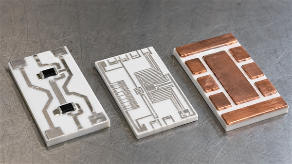
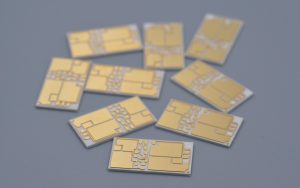
Conceptual alumina circuit samples showing printed conductors, fine thin-film patterns and bonded copper islands

Thick Film on Alumina Substrate

Thick film on alumina substrate uses patterned pastes followed by controlled firing. Conductors and resistors can be integrated on the same ceramic, with additional compatible dielectric layers where required. Our thick-film ceramic PCBs are relevant to hybrid circuits that need printed circuitry rather than a conventional etched copper laminate.

For an alumina substrate resistor circuit, paste selection, firing conditions, geometry and trimming influence final resistance. Material purity alone does not define resistor tolerance or temperature coefficient.

Thin-Film Circuit Patterns

An alumina thin film substrate requires suitable surface quality for deposition and patterning. Our thin-film ceramic PCBs support applications where precise conductor geometry is central to the design. A polished surface may help, but line capability must still be evaluated against the chosen metal stack and production process.

In alumina substrate etching, distinguish patterning the metal layer from machining the ceramic itself. A conductor etchant and a laser used to shape fired ceramic solve different manufacturing problems.

Direct-Bonded Copper and Plated Metallization

Our direct-bonded copper ceramic PCBs combine ceramic insulation with copper conductors for power circuits. DCB, also called DBC, bonds copper foil to the ceramic through a controlled bonding process. DPC instead uses a deposited seed layer and plated copper. Select the route according to conductor geometry, copper requirements and reliability conditions.

A metalized alumina substrate is therefore an incomplete specification. State the conductor material, thickness, adhesion requirements, surface finish and usable circuit area. Heavier copper can improve current handling but also increases thermomechanical stress during temperature changes.

Our DPC ceramic PCB capability includes up to two conductive layers, conductor thickness from 2 to 200 μm and a maximum panel size of 138 × 190 mm. These are process-level capability limits, not a guarantee that every combination is available on every alumina grade or circuit pattern. We confirm the applicable thickness, pattern and panel arrangement for the specific design.

Alumina Substrate vs FR4, AlN and Silicon Nitride

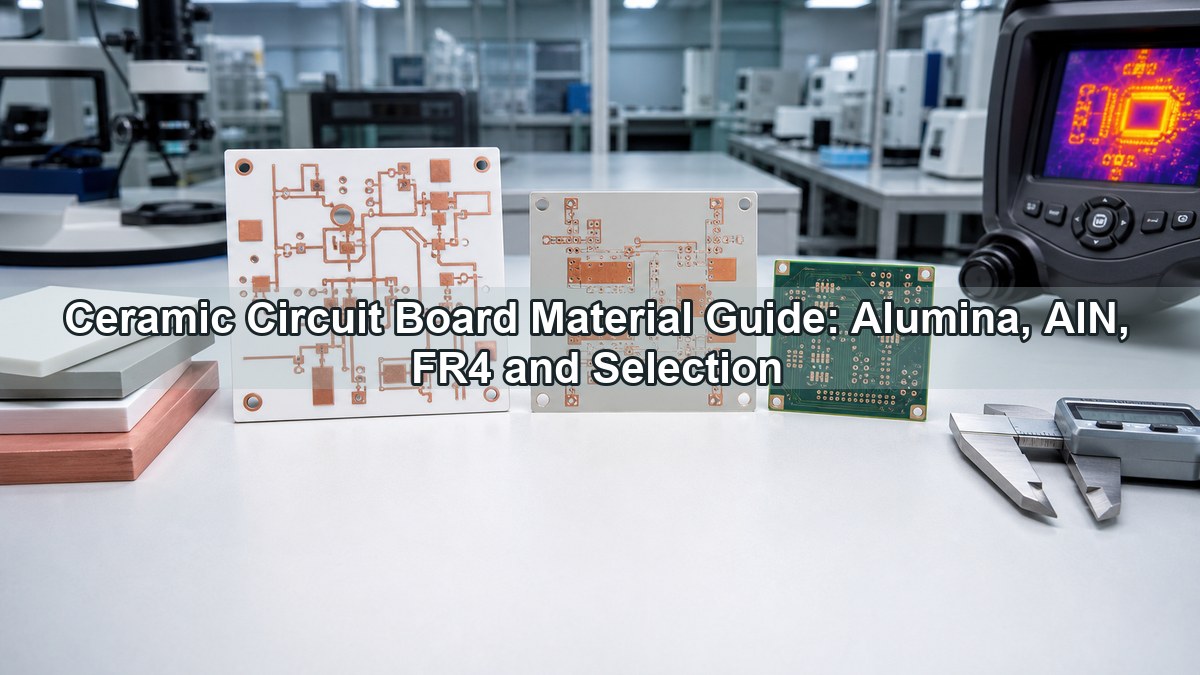
An alumina substrate vs FR4 comparison starts with the circuit’s job: ceramic insulation and heat transfer, or dense multilayer interconnection. Aluminum nitride (AlN) and silicon nitride (Si3N4) address more demanding thermal or mechanical requirements within ceramic power circuits. Typical applications help make those differences concrete.

Material Main selection priority Typical applications
Alumina, Al2O3 Balanced insulation, heat conduction and ceramic processing cost LED circuit substrates, thick-film resistor networks, sensor hybrids and power-module substrates
FR4 Dense multilayer routing and economical general-purpose interconnection Industrial control boards, computer motherboards and network equipment
Aluminum nitride, AlN Higher heat conduction where the ceramic is a thermal bottleneck High-power laser-diode cooling assemblies and high-power-density industrial semiconductor modules
Silicon nitride, Si3N4 Fracture toughness and resistance to repeated thermal cycling EV traction-inverter modules and other power modules with demanding lifetime requirements

Where Are Alumina Ceramic Substrates Used?

What is alumina used for? In electronics, alumina ceramic substrates support circuits that need electrical isolation, controlled conductor patterns and a stable mounting surface. Their role differs by application.

LED Packages and Lighting Modules

Alumina carries the LED’s conductor pads while electrically separating them from the heat sink. Heat passes from the package through its attachment, ceramic and thermal interface. In our high-power LED ceramic PCBs, pad layout, ceramic thickness and mounting flatness must work together. The conceptual cross-section below identifies the ceramic layer in this heat path.
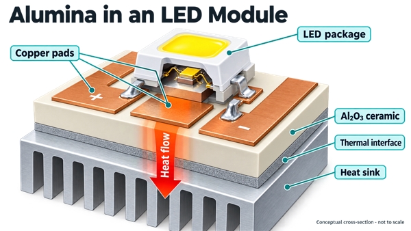
Conceptual LED module cross-section identifying copper pads, Al2O3 ceramic insulation, thermal interface and heat sink

Power Modules and Converter Circuits

In a power module, copper patterns carry current and provide mounting areas for semiconductor devices. The alumina layer separates these live conductors from the cooled base while transferring heat. Copper thickness, conductor spacing and ceramic edge clearance determine the circuit geometry; solder attachment and temperature cycling affect reliability. Our DCB and DPC routes provide different ways to form these copper structures.

Hybrid Circuits and Sensor Electronics

Thick-film hybrids combine conductors and printed resistors on one insulating tile. Automotive sensor interfaces, resistor networks and measurement electronics use this format where compact, stable circuit elements are needed. Alumina supports paste firing and resistor trimming. Paste compatibility, resistor temperature coefficient and the substrate’s flatness are therefore more useful manufacturing inputs than a purity number alone.

RF and Microwave Circuits

An alumina RF substrate can carry thin-film transmission lines, matching networks and resistors in microwave hybrid circuits. For an alumina substrate for high frequency, use alumina substrate permittivity and loss data at the operating frequency, not only the 1 MHz table values. Surface roughness, metal thickness and conductor dimensions affect impedance and loss, making surface preparation and pattern control central to fabrication.

Thermal Printheads

Thermal printheads can use an alumina base with a glazed surface beneath patterned heater resistors. The ceramic provides mechanical support and a heat path, while the glaze helps control heat near the printing elements. Flatness and heater-layer consistency influence printing uniformity. The glaze profile and protective coating are specialized parts of this heater structure, rather than features of an ordinary bare alumina tile.

What Affects Alumina Substrate Price?

Alumina substrate price depends on grade, thickness, dimensions, polishing, holes, edge processing, conductor formation, inspection and order volume. Comparing a blank tile with a finished multilayer hybrid circuit is not a like-for-like cost comparison.

When comparing quotations from alumina substrate suppliers or alumina ceramic substrate manufacturers, separate the alumina sheet price from metallization, tooling, testing and assembly charges. As a China alumina ceramic substrate manufacturer, we quote the agreed ceramic circuit scope and acceptance requirements so you can compare equivalent boards, not a bare tile against a populated assembly.

Why Choose Us as Your Alumina Substrate PCB Manufacturer?

At EBest Circuit (Best Technology), we provide ceramic PCB fabrication and assembly support from prototype requirements to volume production. We match the manufacturing route to your conductor pattern, substrate grade and assembly needs.

  • Process choices matched to the circuit: our ceramic PCB range includes thick-film, thin-film, DCB and DPC options, so conductor structure can be evaluated alongside substrate requirements.
  • Defined manufacturing capability: our DPC process supports the layer, conductor-thickness and panel-size limits described above. Our DCB capability includes up to two layers. Applicable limits remain subject to material selection, board dimensions, circuit complexity and engineering review.
  • Engineering and assembly continuity: we provide DFM review, PCB prototyping, component sourcing and PCB assembly services. The agreed scope depends on the circuit and assembly requirements.

For your next alumina substrate circuit, contact our team at sales@bestpcbs.com to discuss a custom ceramic PCB manufactured for your application.
You may also like

Cost-Effective Al2O3 Ceramic PCB Manufacturer: How to Balance Price, Performance, and Reliability
Friday, July 10th, 2026

What Is an Al2O3 Ceramic PCB?

An Al2O3 ceramic PCB, also called an alumina ceramic PCB, is a printed circuit board or ceramic circuit substrate made from aluminum oxide ceramic. It is used when a design needs better thermal stability, electrical insulation, dimensional stability, and high-temperature resistance than many standard organic PCB materials can provide.

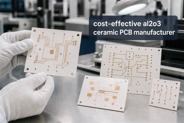
Cost-effective Al2O3 ceramic PCB manufacturer hero image with alumina ceramic PCB substrates

For many electronic products, FR4 PCB is still the most economical PCB material. But when heat, voltage, frequency, size, or reliability requirements become more demanding, alumina ceramic PCB can become a practical and cost-effective option.

The key word is cost-effective, not simply cheap. A low-cost board that fails during assembly or field operation is not economical. A cost-effective Al2O3 ceramic PCB manufacturer should help buyers choose the right ceramic grade, conductor process, copper thickness, tolerance, surface finish, and inspection level for the real application.

Why Choose Al2O3 Instead of Standard FR4?

Al2O3 ceramic PCB is selected when the board material becomes part of the performance requirement. In high-power, high-temperature, high-voltage, compact, or reliability-sensitive designs, the substrate does more than hold copper traces. It affects heat transfer, insulation, mechanical stability, and long-term circuit behavior.

Common reasons to choose Al2O3 ceramic PCB include:

  • Better thermal conductivity than standard FR4
  • Strong electrical insulation
  • Good dimensional stability
  • High operating temperature capability
  • Good mechanical strength
  • Compatibility with thick film, thin film, and DCB ceramic PCB processes
  • Reliable performance in harsh or compact environments

Alumina ceramic PCB is commonly used in LED modules, power electronics, sensors, automotive electronics, industrial control, RF modules, high-voltage circuits, medical electronics, aerospace electronics, and high-reliability assemblies.

Why Al2O3 Is Often More Cost-Effective Than AlN?

Aluminum nitride (AlN) ceramic PCB has higher thermal conductivity than alumina, but it is also usually more expensive. For some power modules and compact thermal designs, AlN is the right choice. However, many products do not need that extra thermal performance.

Al2O3 often gives a better cost-performance balance when the design needs ceramic reliability but does not require the highest possible thermal conductivity.

Material Main Advantage Cost Position Best Fit
Al2O3 ceramic PCB Stable, reliable, widely used, good insulation, practical thermal performance More economical ceramic option LED, sensors, power electronics, RF modules, industrial electronics
AlN ceramic PCB Much higher thermal conductivity Higher cost High-power modules, compact heat-critical designs, advanced thermal products
FR4 PCB Lowest cost for many standard circuits Most economical General control boards, consumer electronics, low-thermal-stress products
Metal core PCB Good heat spreading with metal base Often economical for LED and power boards LED lighting, power conversion, thermal management products

If a design can meet thermal and electrical requirements with Al2O3, choosing AlN may increase cost without improving the product in a meaningful way. A good ceramic PCB manufacturer should help customers avoid over-specification.

What Makes an Al2O3 Ceramic PCB Cost-Effective?

A cost-effective ceramic PCB is not defined by substrate price alone. The total cost includes material, process complexity, yield, testing, lead time, assembly compatibility, and long-term reliability.

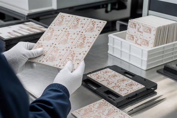
Alumina ceramic PCB panels being reviewed during production preparation

Important cost drivers include:

  • Ceramic substrate size and thickness
  • Alumina purity, such as 96% or 99% Al2O3
  • Circuit size and panel utilization
  • Conductor material and thickness
  • Thick film, thin film, or DCB process selection
  • Minimum line width and spacing
  • Hole, via, and edge requirements
  • Copper thickness or metallization thickness
  • Surface finish and solderability requirement
  • Tolerance level
  • Quantity and delivery schedule
  • Electrical test, visual inspection, and reliability test requirements
  • Whether PCB assembly or wire bonding is needed

The most cost-effective design is usually the one that matches the process capability without adding unnecessary tolerances. For example, asking for extremely fine lines, tight dimensional control, or special metallization may be necessary in some circuits, but it should be justified by the application.

Main Manufacturing Options for Al2O3 Ceramic PCB

Al2O3 ceramic PCB can be manufactured through different processes. The right process depends on circuit density, current load, thermal demand, conductor material, and budget.

Thick Film Al2O3 Ceramic PCB

Thick film ceramic PCB uses screen printing to apply conductive paste onto the ceramic substrate, followed by high-temperature firing. Silver palladium, gold palladium, or other conductor systems may be used depending on the design.

Thick film is often cost-effective for sensors, hybrid circuits, high-temperature electronics, and moderate-density ceramic circuits. It is useful when the design needs ceramic stability but does not require extremely fine thin-film precision.

Thin Film Al2O3 Ceramic PCB

Thin film ceramic PCB uses deposited metal layers and photolithography-like processes to create finer and more precise circuit features. It can support tighter line width, spacing, and high-frequency performance compared with many thick film structures.

Thin film Al2O3 ceramic PCB is usually selected when precision is more important than lowest cost. It is common in RF, microwave, sensor, and high-accuracy electronic modules.

DCB Al2O3 Ceramic PCB

DCB ceramic PCB means direct copper bonded ceramic PCB. In this process, copper is bonded directly to the ceramic substrate under high temperature. DCB ceramic PCB is often used in power electronics because it provides good current capacity, thermal transfer, and reliability.

DCB Al2O3 ceramic PCB can be cost-effective for power modules when the design needs stronger copper and better heat transfer than thick film can provide.

Al2O3 Ceramic PCB Applications

Al2O3 ceramic PCB is used across many industries because it combines ceramic stability with practical manufacturing cost.

Common applications include:

  • LED lighting modules
  • Power supply modules
  • IGBT and MOSFET power circuits
  • Automotive electronics
  • Industrial control boards
  • High-temperature sensors
  • Medical electronic modules
  • RF and microwave circuits
  • Aerospace electronics
  • High-voltage insulation circuits
  • Laser diode modules
  • Battery management and energy equipment

For each application, the board structure should be reviewed against real working conditions. A sensor circuit, LED module, and power module may all use Al2O3, but the conductor process and inspection requirements can be very different.

How to Reduce Cost Without Reducing Reliability?

Buyers can reduce ceramic PCB cost by making the design easier and more stable to manufacture. This does not mean lowering quality. It means removing unnecessary complexity.

Practical cost-saving steps include:

  • Choose Al2O3 instead of AlN when thermal requirements allow it
  • Use standard substrate thickness when possible
  • Avoid overly tight tolerances unless the design needs them
  • Keep board outline simple when possible
  • Improve panel utilization
  • Confirm realistic line width and spacing
  • Avoid unnecessary surface finish requirements
  • Clarify whether thick film, thin film, or DCB is actually needed
  • Separate prototype goals from mass production requirements
  • Provide complete files at the quotation stage
  • Discuss assembly requirements before finalizing the PCB design

The supplier should review manufacturability before production. A small design change may improve yield and reduce cost without changing circuit performance.

How to Evaluate an Al2O3 Ceramic PCB Manufacturer?

When choosing a cost-effective Al2O3 ceramic PCB manufacturer, buyers should evaluate both price and engineering capability.

Useful supplier checks include:

  • Experience with alumina ceramic PCB projects
  • Ability to support thick film, thin film, or DCB ceramic PCB
  • Clear material options, such as 96% or 99% alumina
  • Understanding of thermal, insulation, and tolerance requirements
  • DFM review before production
  • Stable quality control for metallization, adhesion, surface finish, and dimensional accuracy
  • Electrical testing and visual inspection capability
  • Prototype and mass production support
  • PCB assembly or ceramic PCBA support if needed
  • Clear communication about lead time, process limits, and cost trade-offs

The best supplier is not always the one with the lowest first quote. It is the one that can produce the board correctly, explain cost drivers, prevent avoidable defects, and support the project from prototype to production.

What to Send for an Al2O3 Ceramic PCB Quote?

A complete RFQ helps the manufacturer quote faster and more accurately. It also reduces the risk of wrong material, wrong process, or wrong tolerance assumptions.

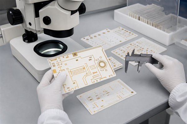
Al2O3 ceramic PCB quality inspection with microscope and caliper

For a ceramic PCB quote, provide:

  • Gerber files
  • Drawing or mechanical outline
  • Ceramic material, such as Al2O3
  • Alumina purity if specified
  • Substrate thickness
  • Board dimensions
  • Copper or conductor thickness
  • Thick film, thin film, or DCB process requirement if known
  • Minimum line width and spacing
  • Hole, slot, or edge metallization requirements
  • Surface finish
  • Working voltage and current
  • Thermal requirement or power dissipation
  • Operating temperature range
  • Quantity for prototype and mass production
  • Inspection or reliability test requirement
  • Assembly requirement if PCBA is needed

If you are not sure which process is best, explain the application and performance target. A qualified ceramic PCB manufacturer can help compare thick film, thin film, DCB, Al2O3, AlN, FR4, and metal core PCB options.

When Al2O3 Ceramic PCB May Not Be the Best Choice?

Al2O3 is versatile, but it is not always the right answer.

FR4 may be better when the circuit is low-power, low-temperature, and cost-sensitive. Metal core PCB may be better for some LED and power designs that need heat spreading but do not need ceramic insulation or high-temperature stability. AlN may be better when thermal conductivity is the main limiting factor and the product can justify higher cost.

The goal is not to force every project into alumina ceramic PCB. The goal is to choose the most reliable and economical structure for the real design.

How EBest Circuit Supports Cost-Effective Ceramic PCB Projects?

EBest Circuit (Best Technology) provides custom PCB and PCBA solutions including ceramic PCB, metal core PCB, FR4 PCB, rigid-flex PCB, high frequency PCB, heavy copper PCB, HDI PCB, component sourcing, PCB assembly, and full turnkey service.

For ceramic PCB, EBest Circuit supports alumina ceramic PCB and other ceramic substrate solutions for customers that need thermal stability, insulation, and reliability. The team can review ceramic material, process choice, manufacturability, PCB assembly requirements, and quotation details before production.

This is useful for buyers who want one engineering conversation covering bare ceramic PCB, material selection, process selection, assembly risk, lead time, and cost control.

FAQ

What is an Al2O3 ceramic PCB?

An Al2O3 ceramic PCB is a printed circuit board or circuit substrate made from aluminum oxide ceramic. It is used when the design needs strong insulation, thermal stability, dimensional stability, and reliability in demanding environments.

Is Al2O3 ceramic PCB cost-effective?

Yes, Al2O3 ceramic PCB can be cost-effective when the design needs ceramic performance but does not require the higher thermal conductivity and higher cost of AlN ceramic PCB.

What is the difference between Al2O3 and AlN ceramic PCB?

Al2O3 is usually more economical and widely used. AlN has much higher thermal conductivity but is more expensive. The right choice depends on thermal demand, budget, application, and reliability requirements.

Which is cheaper, Al2O3 ceramic PCB or FR4 PCB?

FR4 is usually cheaper for standard circuits. Al2O3 ceramic PCB is used when FR4 cannot meet thermal, insulation, temperature, or reliability requirements.

What affects the price of Al2O3 ceramic PCB?

Price is affected by material grade, substrate thickness, board size, process type, conductor thickness, line width, spacing, holes, tolerance, quantity, testing, lead time, and assembly requirements.

What is the best process for alumina ceramic PCB?

There is no single best process for every design. Thick film is often practical and cost-effective, thin film is better for fine precision and RF needs, and DCB is suitable for higher-current power applications.

Can Al2O3 ceramic PCB be used for high-temperature electronics?

Yes. Alumina ceramic PCB is commonly used in high-temperature and harsh-environment electronics because of its ceramic stability, insulation properties, and thermal performance.

Can a ceramic PCB manufacturer also provide assembly?

Some manufacturers can provide ceramic PCB assembly or turnkey PCBA support. This is useful when the project needs component sourcing, SMT, wire bonding, testing, or production integration.

Conclusion

A cost-effective Al2O3 ceramic PCB manufacturer should help you balance price, process capability, thermal performance, insulation, reliability, and production yield. Alumina ceramic PCB is often the practical ceramic choice when FR4 is not enough and AlN is more than the application requires.

If you need an Al2O3 ceramic PCB, thick film ceramic PCB, thin film ceramic PCB, DCB ceramic PCB, or ceramic PCBA solution, EBest Circuit (Best Technology) can review your files and help choose a reliable manufacturing path. Contact sales@bestpcbs.com for a quotation and engineering review.

You may also like

Why don’t use BeO as substrate to make DBC ceramic PCB?
Monday, June 22nd, 2020

It is widely known that BeO with high thermal conductivity (200-250W/m.k). High dielectric constant 6-7 (0.1MHz) and dielectric loss tangent is 10-4 (0.1GHz), extremely high working temprature. It is ideal material for ceramic PCB, lots of engineers want to use it as DBC ceramic PCB substrate.

But it is not popular in ceramic PCB market, comparing with Al2O3, AIN, Si3N4, or ZrO2, as the powder of BeO is extremely poisonous.

The poison gas is produced by the reaction between oxygen, Cu and BeO under 1065-1085 degrees Celsius, so it is limited to make cooper on BeO substrate, it has caused ALN (Aluminium Nitride) is becoming more and more popular.

Right now, only few countries are using BeO to make ceramic PCB, such as USA, Russia and China. USA had biggest capability to make BeO , and here in China, there’re still some companies to make BeO raw material and among them, a few companies to produce direct copper bonded (DCB) on BeO because of environment limitation.

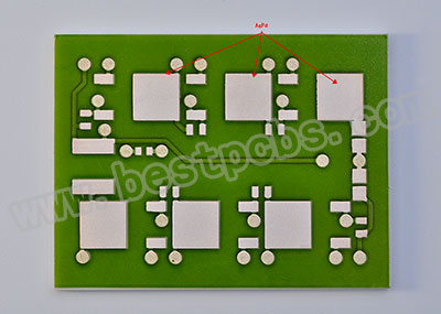
Though BeO is not popular for DBC technology, but it is feasible for thick film technology, because when the mentalization of Ceramic PCB, the conductor (Au or AgPd) on BeO substrate was made by silk-screen printing, and drying temperature is only around 850C, no need to under high temperature environment, so there is no chemical reactions, no environment issue.

Below the thick film ceramic PCB manufacturing process for your reference.

https://www.bestpcbs.com/products/thick-film-ceramic-pcb-manufacturing-process.htm

Here is the photo of BeO with AgPd conductor.

BeO with AgPd conductor

Welcome to contact us if you have better idea, or different comments on BeO ceramic PCB, communation will make us becoming better and better.

You may also like