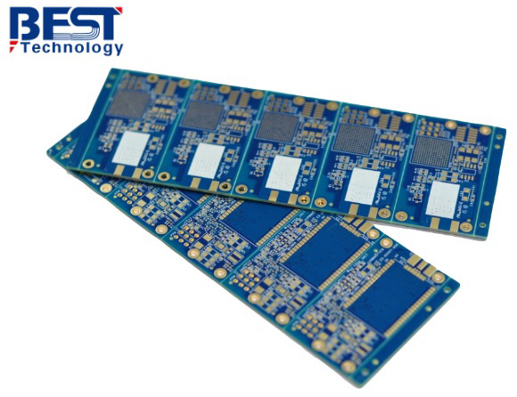
Industrial systems operate in harsh environments. Heat, vibration, dust, moisture, and electrical noise are part of daily life. The circuit boards inside these systems must survive years of continuous duty. This is where industrial PCB manufacturing stands apart from standard consumer production.
In this guide, we will walk through the materials, design rules, process steps, cost structure, certifications, and real-world expectations behind industrial-grade boards. If you design, source, or manage projects in this field, this article will give you clarity and confidence.
What Is Industrial PCB Manufacturing?
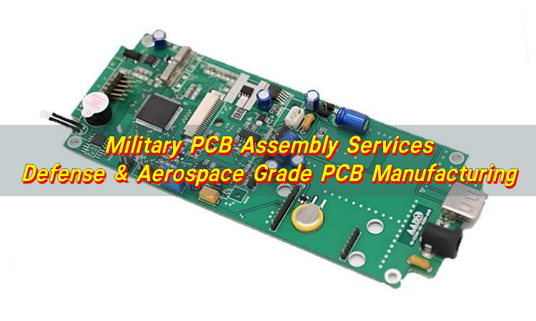
Industrial PCB manufacturing refers to the fabrication and assembly of circuit boards designed for high-reliability, long-life, and high-stress environments. These boards are used in equipment that runs factories, power plants, transportation systems, and heavy machinery.
Unlike consumer electronics, industrial products often:
- Operate 24/7
- Face extreme temperatures
- Handle high voltages or heavy current
- Experience mechanical vibration
- Require a long service life, often 10–20 years
Because of this, the production standards are stricter. Material selection is more demanding. Inspection levels are higher. Traceability is critical.
An industrial board is not defined by size or layer count. It is defined by performance expectations. A simple two-layer board can be industrial if it must operate reliably inside a motor control cabinet for fifteen years.
What Materials Are Used In Industrial PCB Manufacturing?
Material choice drives long-term performance. Industrial boards rarely rely on basic FR-4 alone. Instead, engineers consider thermal stress, mechanical load, and electrical safety margins.
Here are common materials used:
- High-Tg FR-4: Glass transition temperature above 170°C. Ideal for thermal cycling.
- Polyimide: Excellent thermal resistance and chemical stability.
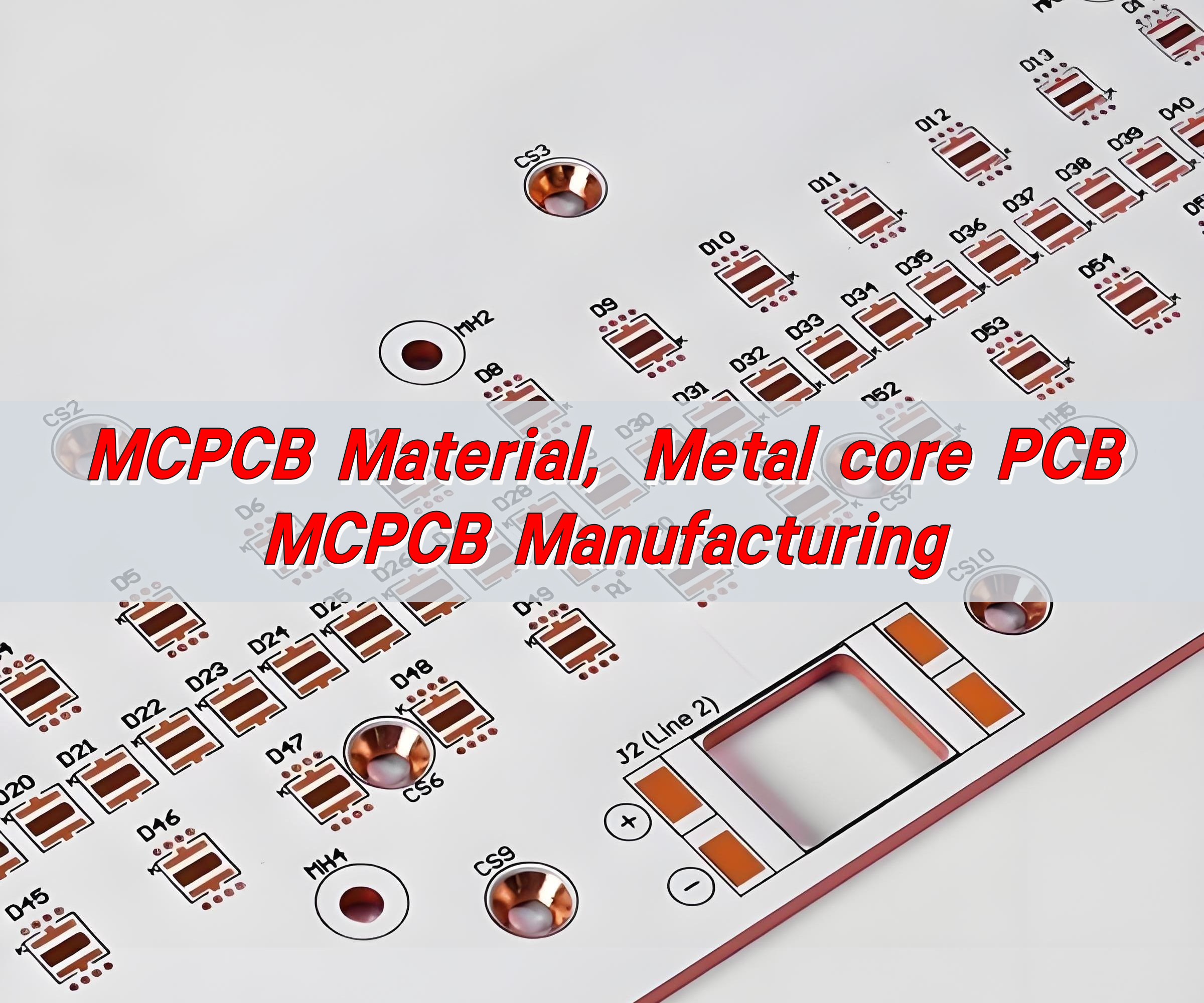
- Metal-core PCB (MCPCB): Aluminum or copper base for heat dissipation.
- Ceramic substrates: Alumina or aluminum nitride for extreme heat and power modules.
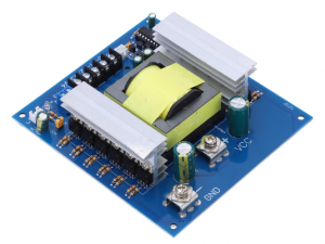
- Heavy copper laminates: 2oz to 6oz copper for high current paths.
Let’s compare common substrate options:
| Material Type | Heat Resistance | Mechanical Strength | Cost Level | Typical Use Case |
| Standard FR-4 | Moderate | Good | Low | Light industrial |
| High-Tg FR-4 | High | Very good | Medium | Motor drives |
| Polyimide | Very high | Excellent | High | Aerospace-grade industrial |
| Aluminum Core PCB | High | Strong | Medium | LED power modules |
| Ceramic PCB | Extreme | Very rigid | High | Power electronics |
Copper thickness is another key factor. Industrial boards often use:
- 2oz copper for power control
- 3oz or 4oz for heavy current
- Thicker copper for busbar-like layers
Surface finish is selected for durability. ENIG, immersion silver, and OSP are common. For long storage, ENIG remains a strong option.
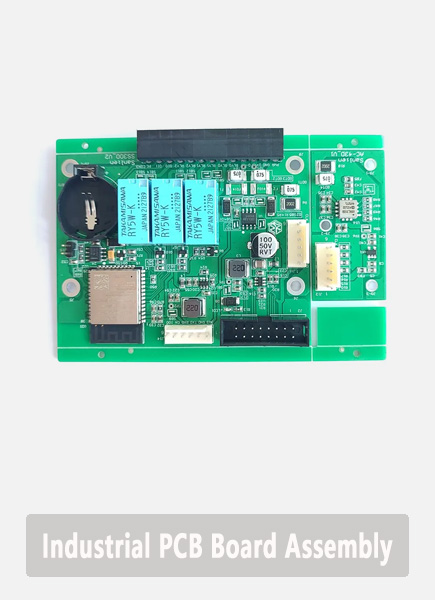
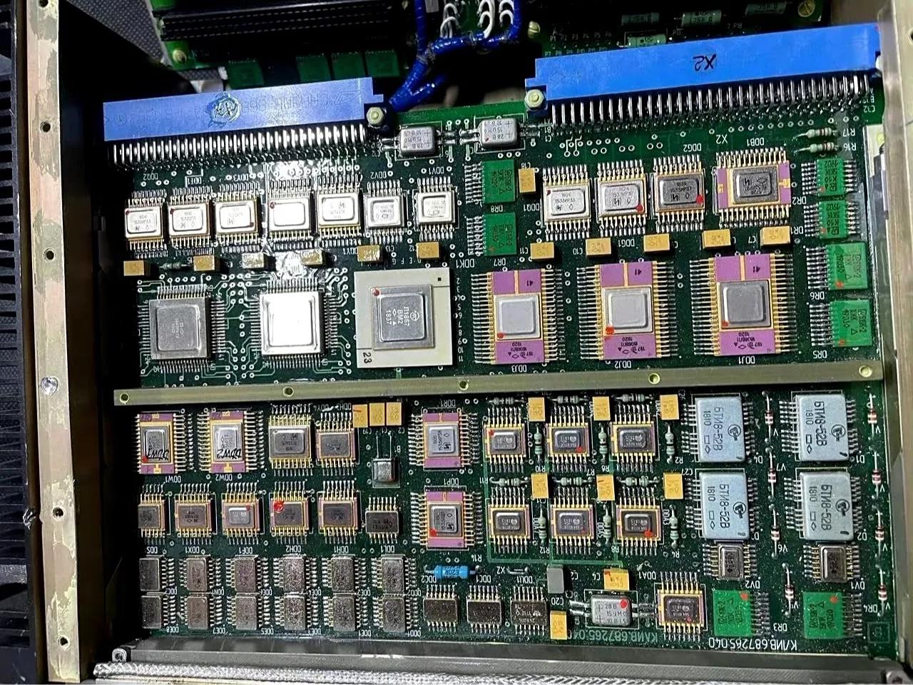
What Industries Use Industrial PCBs?
Industrial PCBs support mission-critical sectors. Because downtime is costly, reliability becomes a core requirement.
Key industries include:
- Factory automation
- Renewable energy systems
- Oil and gas control platforms
- Rail transportation
- Power distribution equipment
- Robotics systems
- Industrial IoT infrastructure
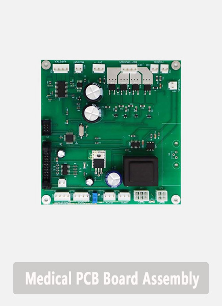
- Medical industrial equipment
For example, motor drives rely on thick copper traces for switching stability. Similarly, solar inverters demand thermal resilience during constant power conversion. In rail systems, vibration resistance is essential for passenger safety.
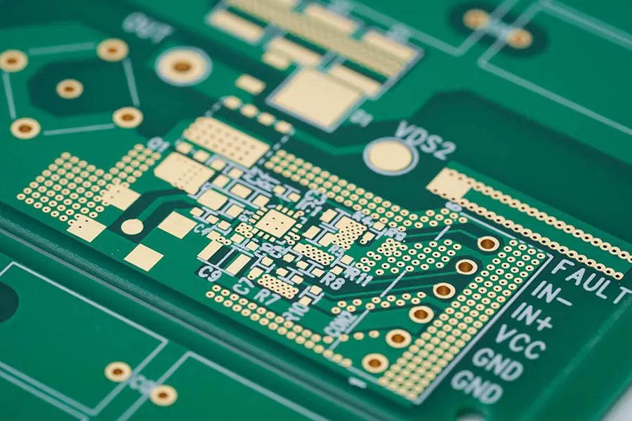
Industrial PCB Design Rules
- Trace Width and Spacing: High-current paths require wider traces. Voltage clearance must meet safety standards.
- Copper Weight Selection: Choose copper thickness based on current load and temperature rise calculations.
- Creepage and Clearance: Industrial boards must meet international safety spacing standards.
- Thermal Management: Use thermal vias, copper pours, and metal cores when necessary.
- Vibration Reinforcement: Anchor large components and connectors.
- Layer Stack-up Planning: Balanced stack-ups reduce warpage.
- Surface Finish Selection: ENIG, OSP, or Immersion Tin depending on application.
Design for manufacturability (DFM) reviews are critical. Best Technology performs DFM checks before fabrication begins. Early feedback reduces rework and accelerates production.
How Long Does Industrial PCB Manufacturing Take?
Lead time depends on complexity, testing scope, and material sourcing. However, planning can significantly improve schedule predictability. Below is a typical timeline for medium-complexity industrial boards:
| Production Stage | Typical Duration |
| Engineering Review | 1–2 days |
| Material Preparation | 2–3 days |
| PCB Fabrication | 7–14 days |
| Assembly (SMT + THT) | 3–7 days |
| Testing & Inspection | 2–5 days |
Best Technology offers expedited services for urgent industrial projects. If your project requires urgent processing, please contact our team immediately or make a note in the order.
Industrial PCB Manufacturing Process
Unlike standard commercial boards, industrial-grade circuits must perform in environments where heat, vibration, dust, and electrical stress are part of daily operation. Because of that, every stage in the process is carefully managed and documented.
Below is a whole process of how a high-reliability industrial PCB moves from design to a fully tested finished board.
1. Engineering Review and DFM Verification
The process begins with a complete review of design files, including Gerber data, drill files, stack-up details, and fabrication notes. Engineers perform Design for Manufacturability (DFM) analysis to identify potential production risks.
Key checks include:
- Trace width and spacing compliance
- Copper weight accuracy
- Annular ring tolerances
- Via structure validation
- Creepage and clearance verification
- Material compatibility
At Best Technology, this stage is critical because catching issues early prevents delays, rework, and unexpected cost increases later in the production cycle.
2. Material Preparation
Once files are approved, raw materials are prepared. Industrial boards often use high-Tg laminates, heavy copper foils, or specialized substrates such as metal cores.
Material preparation includes:
- Cutting laminate panels to production size
- Cleaning copper surfaces
- Verifying material certifications
- Baking moisture-sensitive laminates when required
Proper material handling ensures dimensional stability and strong layer bonding in later stages.
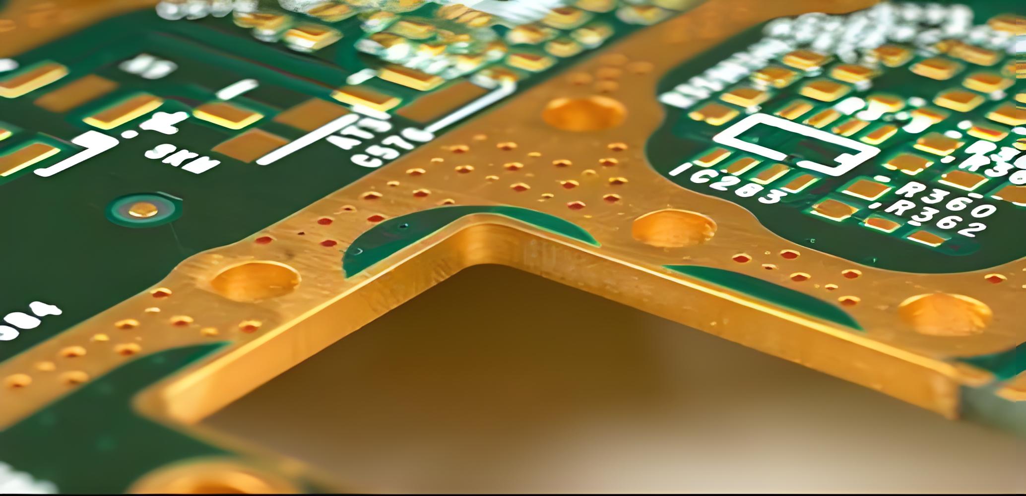
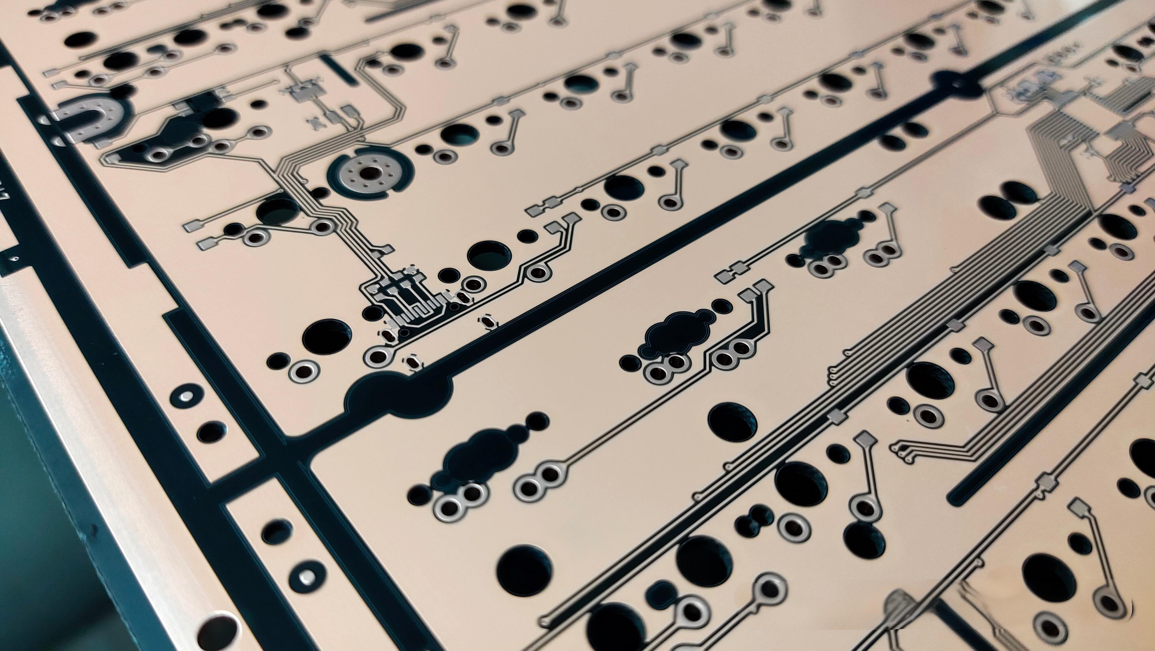
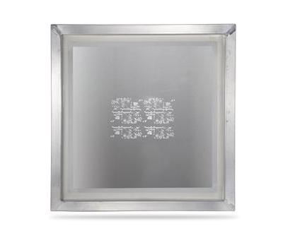
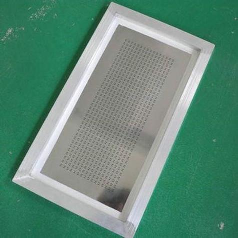
3. Inner Layer Imaging
For multilayer boards, the process starts with inner layers. A photosensitive film is applied to copper-clad laminate panels. The circuit pattern is transferred using UV exposure through phototools.
After exposure, the panel is developed, leaving only the intended copper pattern protected.
Precision at this stage directly impacts electrical performance and layer alignment accuracy.
4. Inner Layer Etching
The exposed copper is removed through controlled chemical etching. This step defines the actual copper traces that carry current within the board.
Strict control of etching parameters ensures:
- Accurate trace width
- Clean copper edges
- Minimal undercutting
- Consistent impedance performance
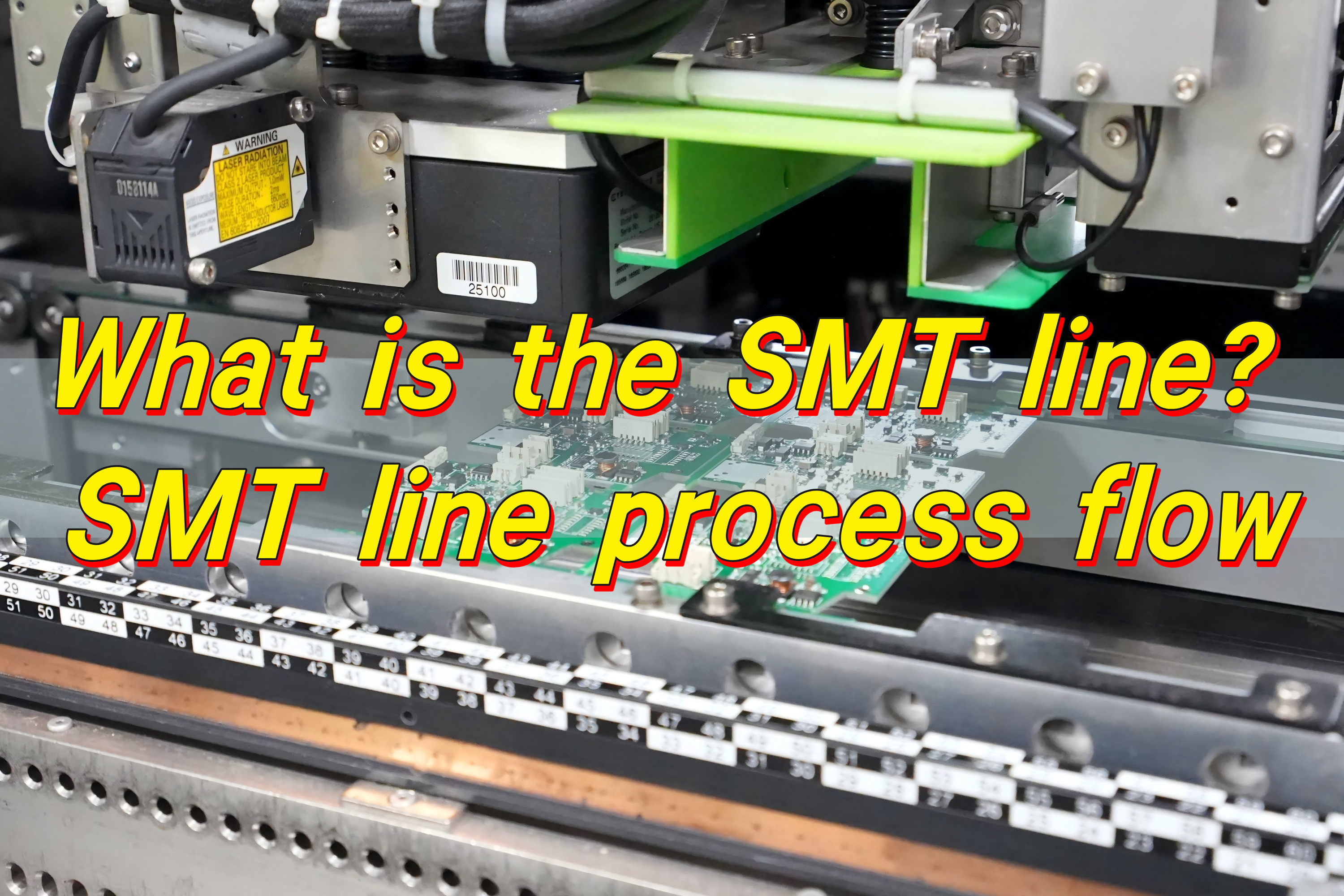
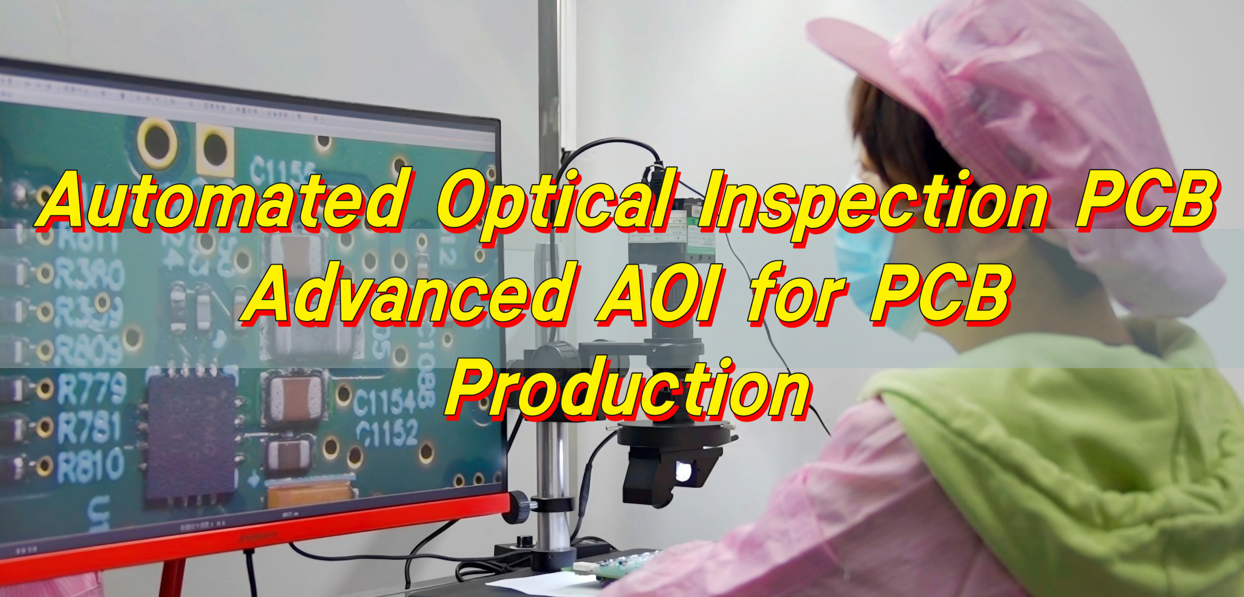
Once etched, each inner layer undergoes automated optical inspection (AOI) to verify pattern accuracy before proceeding.
5. Layer Alignment and Lamination
Next, inner layers are stacked with prepreg sheets and outer copper foils. Proper alignment is essential for via accuracy and structural stability.
The stacked layers are pressed under high heat and pressure in a lamination press. During this stage:
- Resin flows and bonds layers together
- Air pockets are eliminated
- Structural integrity is formed
Balanced stack-up design helps reduce warpage and improves mechanical strength, which is especially important in industrial environments.
6. Drilling
After lamination, mechanical drilling creates vias, component holes, and mounting holes. In advanced designs, laser drilling may be used for microvias.
Drilling accuracy affects:
- Electrical connectivity
- Structural reliability
- Vibration resistance
Hole wall quality is closely inspected because poor drilling can weaken plating performance.
7. Hole Wall Plating
To make vias conductive, the hole walls are chemically treated and plated with copper. This step creates electrical connections between layers.
The plating process includes:
- Desmearing and surface conditioning
- Electroless copper deposition
- Electrolytic copper plating
For industrial boards, thicker copper plating improves mechanical strength and long-term reliability under thermal cycling.
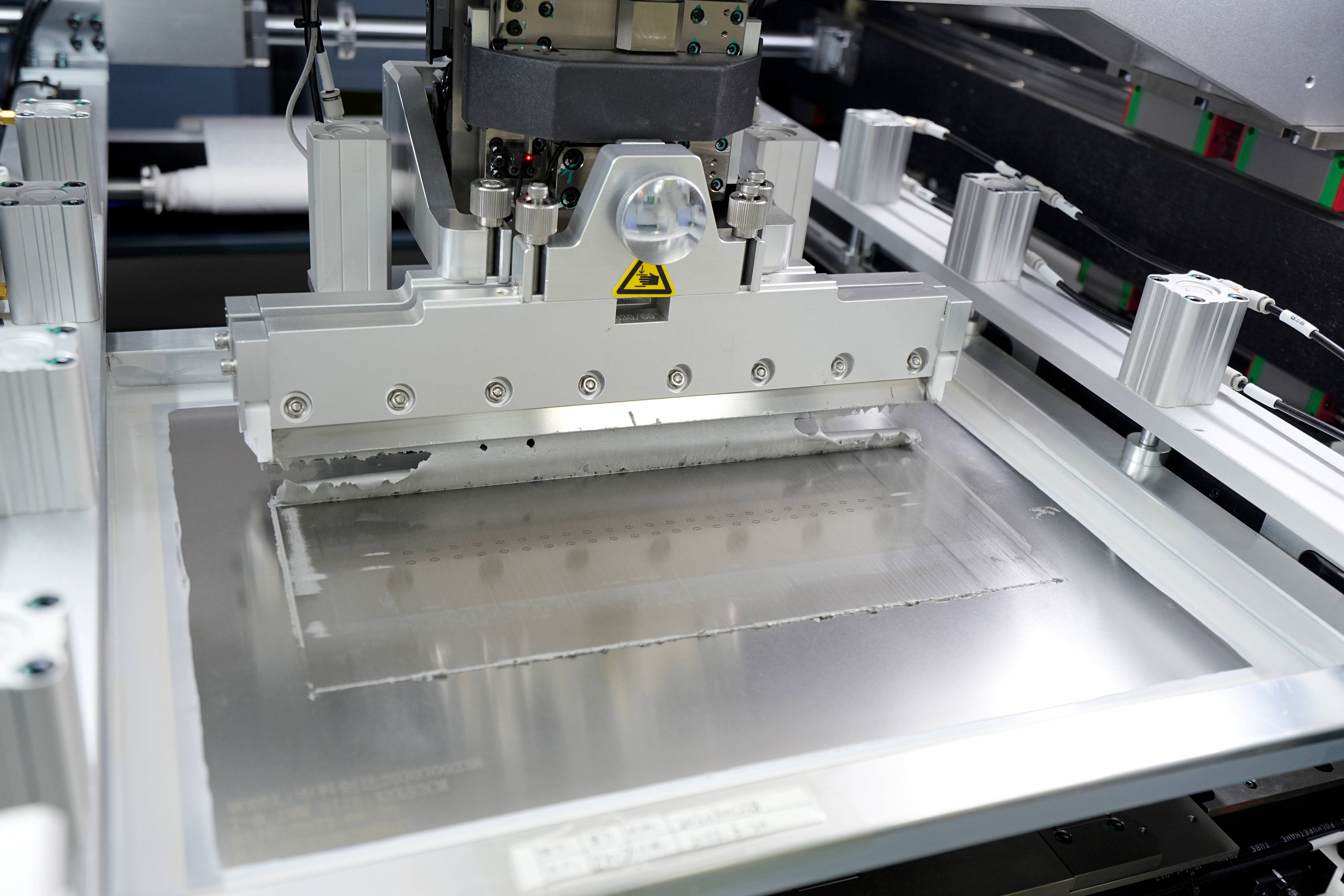
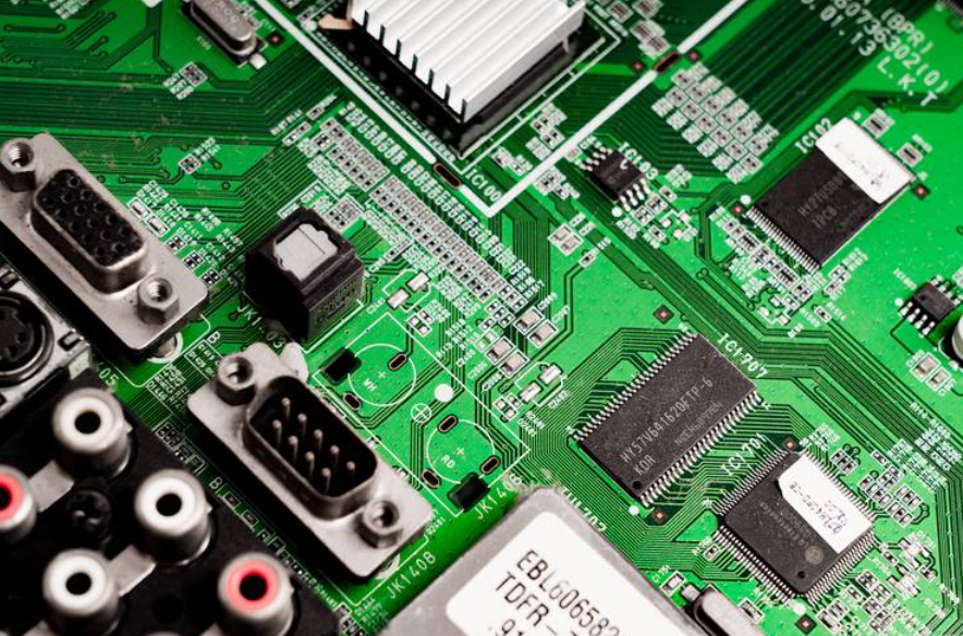
8. Outer Layer Imaging and Etching
The outer layers follow a similar imaging and etching process as the inner layers. Circuit patterns are transferred and defined with high precision. Because outer layers interface directly with components, accuracy here is critical for solder joint reliability and assembly performance.
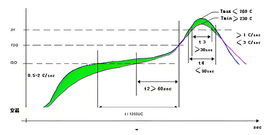
9. Solder Mask Application
A protective solder mask coating is applied over the board surface. It shields copper traces from oxidation and prevents solder bridging during assembly.
Industrial boards may use thicker or higher-grade solder mask formulations for improved environmental resistance. After application, the mask is cured under controlled temperature conditions.
10. Surface Finish Application
The exposed copper pads receive a surface finish to protect against oxidation and ensure reliable soldering.
Common finishes in industrial PCB manufacturing include:
- ENIG (Electroless Nickel Immersion Gold)
- HASL (Hot Air Solder Leveling)
- Immersion Silver
- OSP (Organic Solderability Preservative)
ENIG is widely chosen for industrial applications due to its flat surface and long shelf life.
11. Silkscreen Printing
Component reference markings, logos, and identification codes are printed on the board surface. Clear marking improves traceability and simplifies maintenance during field service.
Industrial systems often require serial numbers or batch tracking information for long-term support.
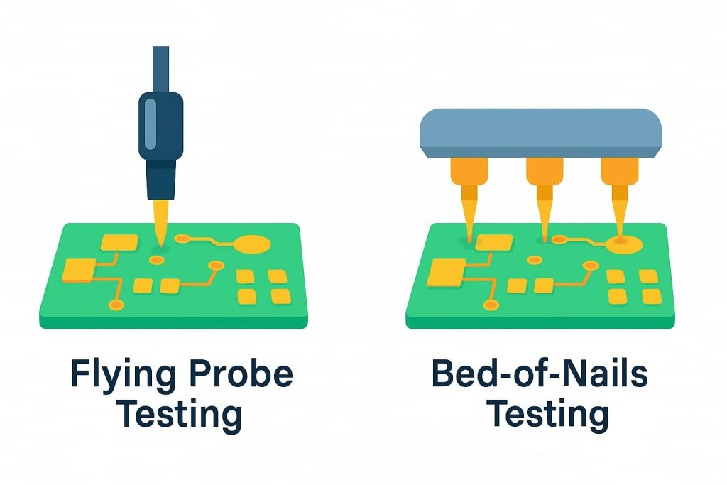
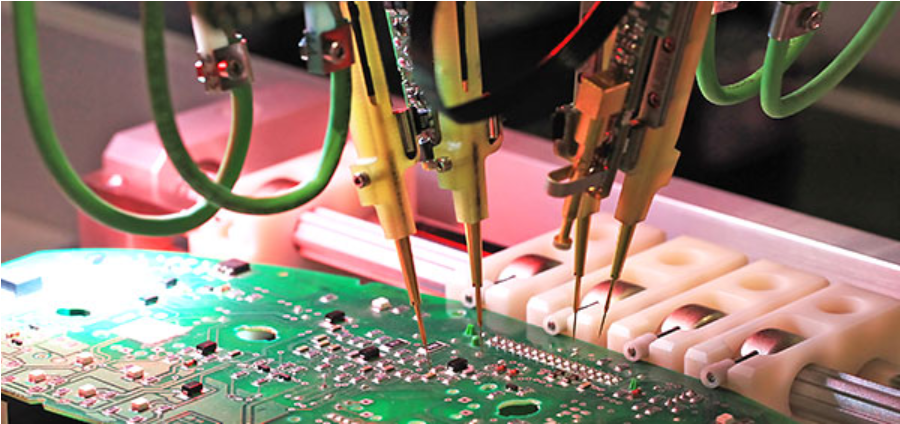
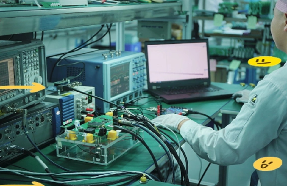
12. Electrical Testing
Every industrial PCB undergoes electrical testing before shipment. Flying probe or fixture-based testing verifies:
- Continuity
- Isolation
- Short circuit detection
- Open circuit detection
Given the critical nature of industrial electronics, 100% testing is standard practice.
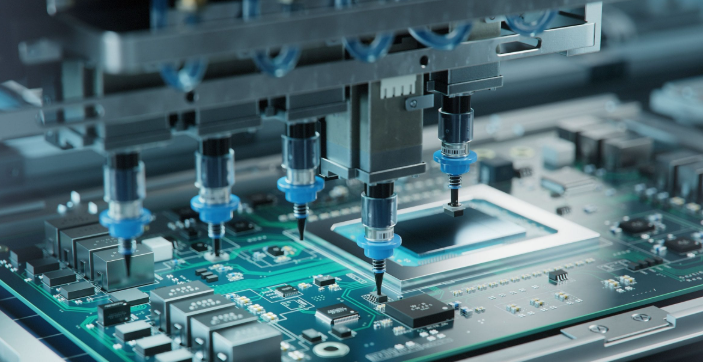
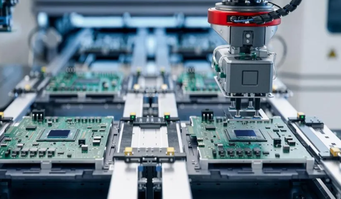
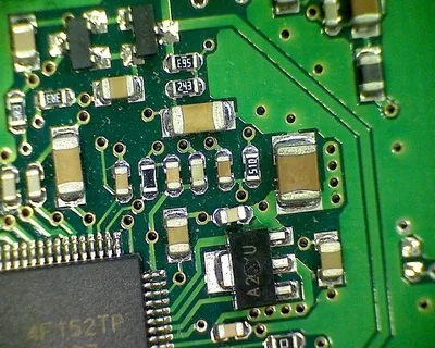
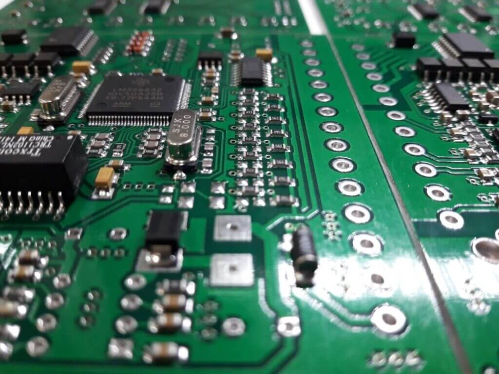
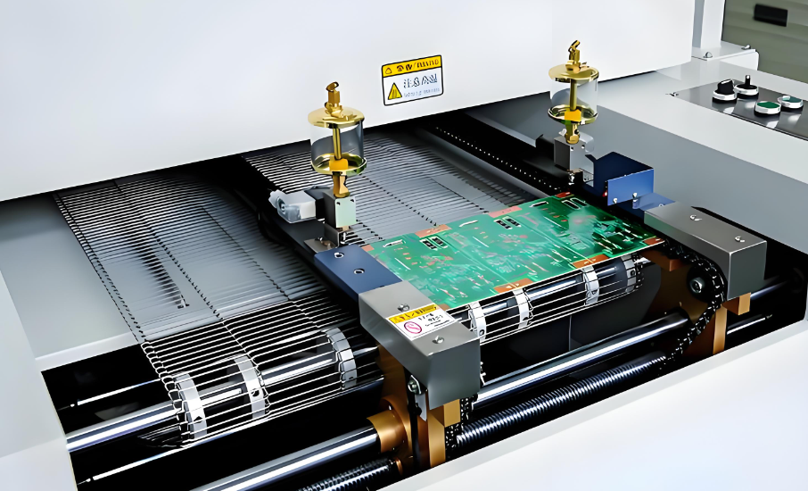
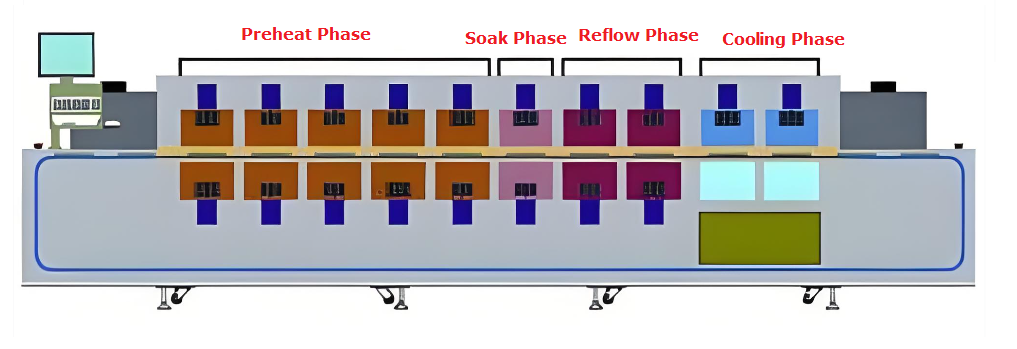
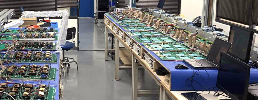
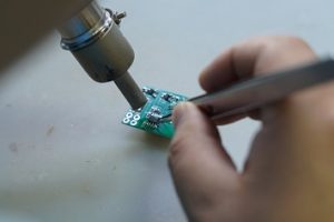
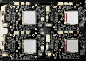
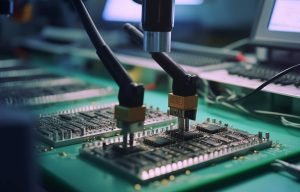
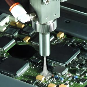
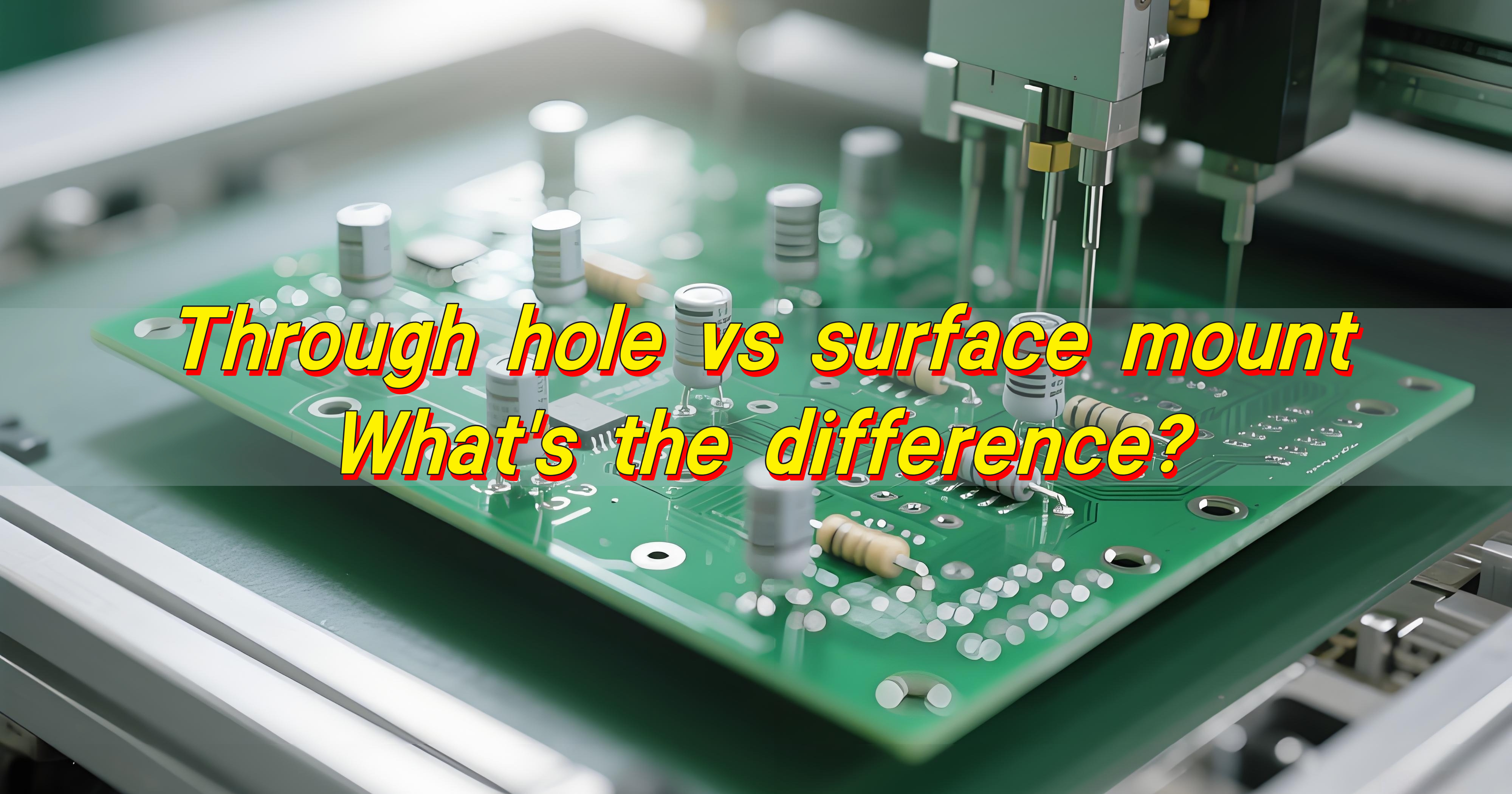
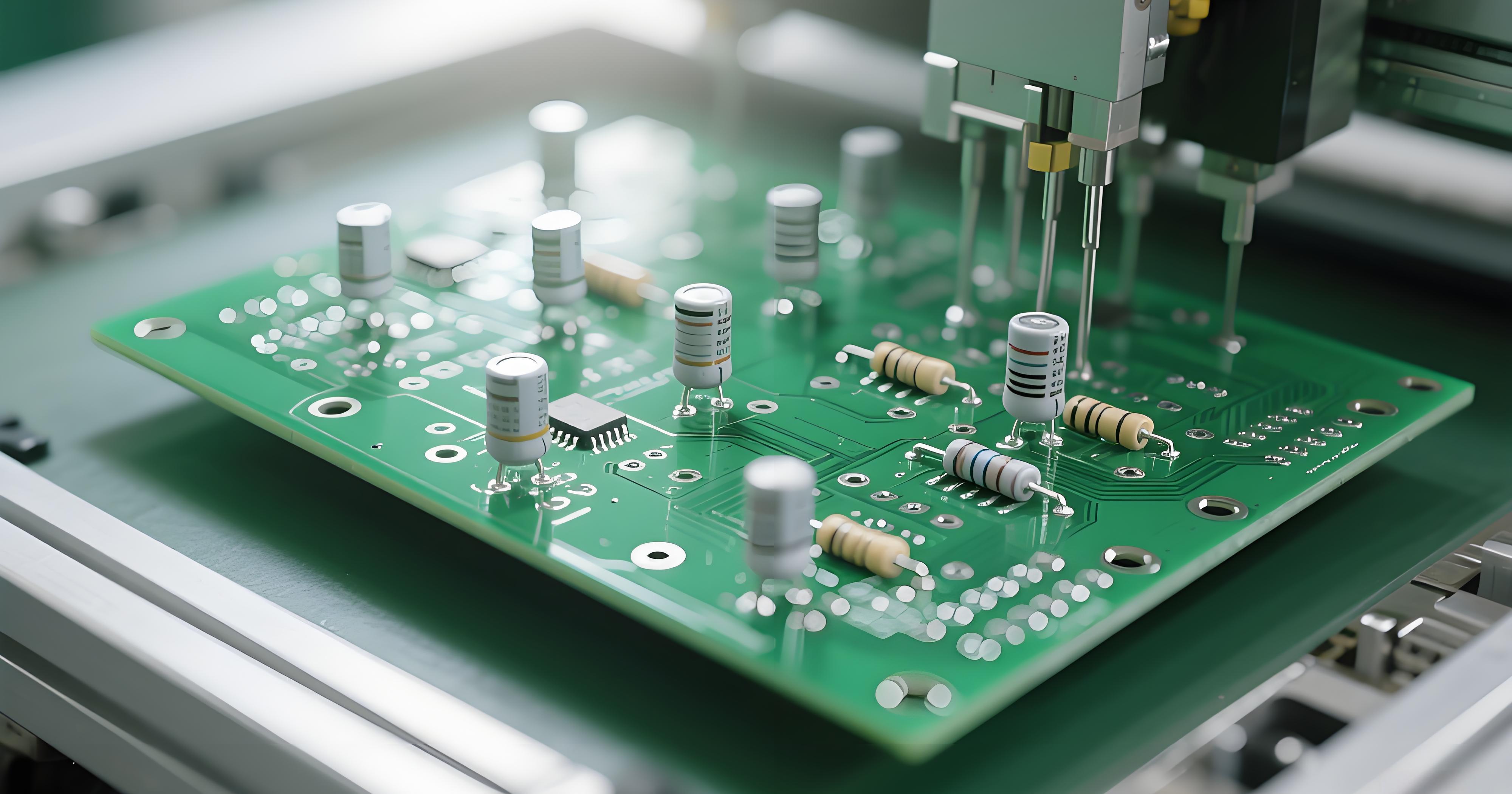
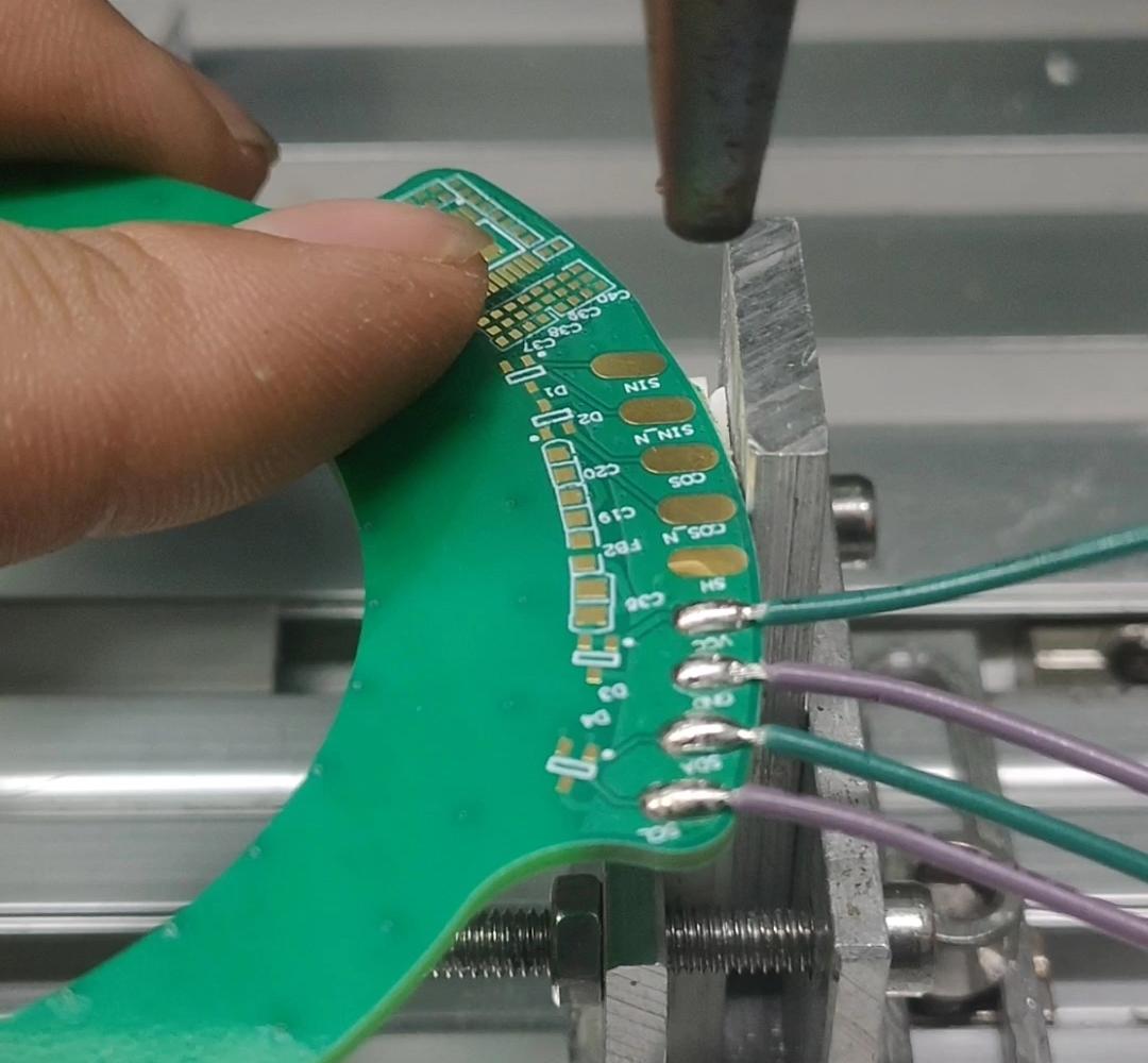
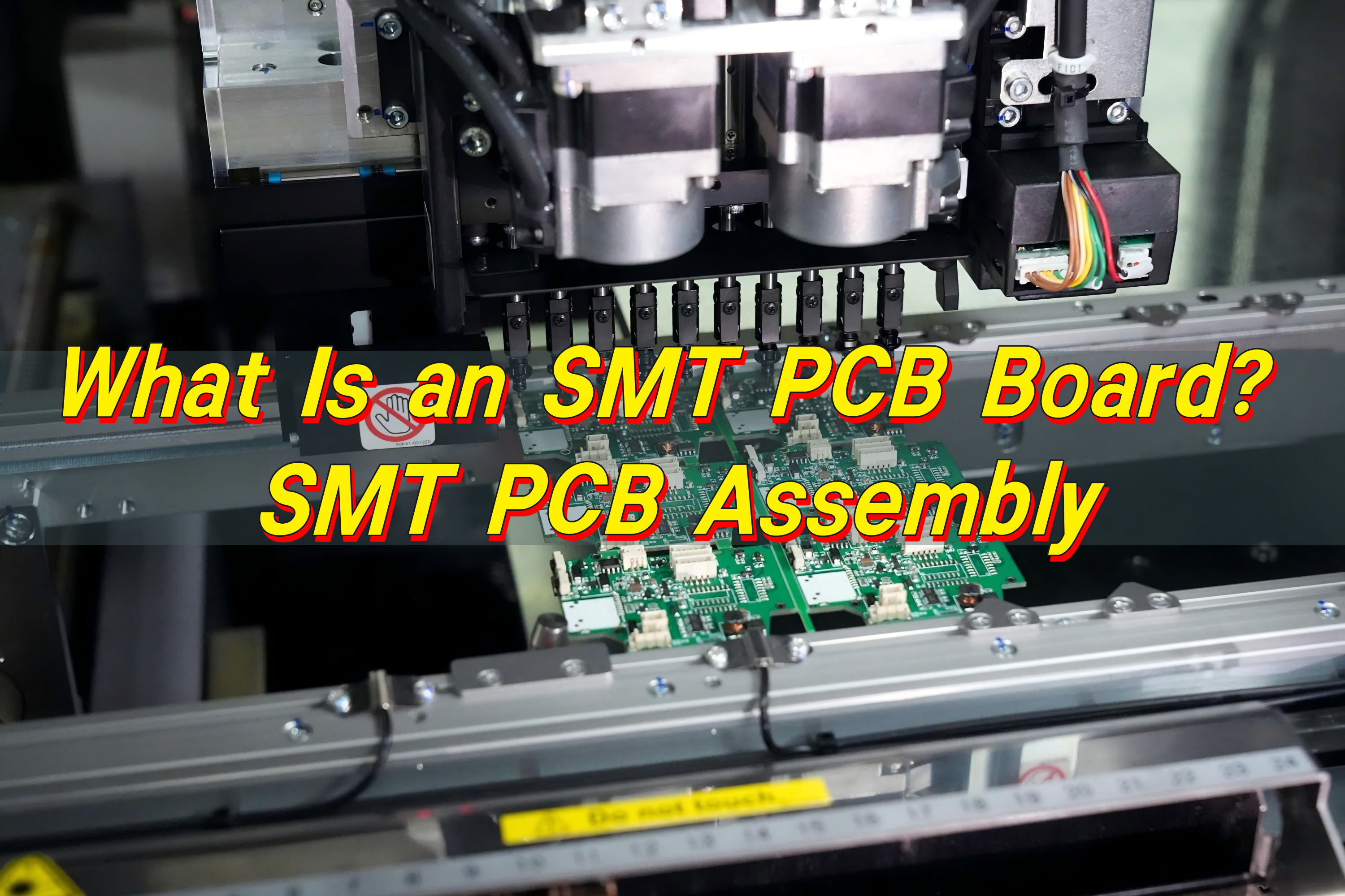
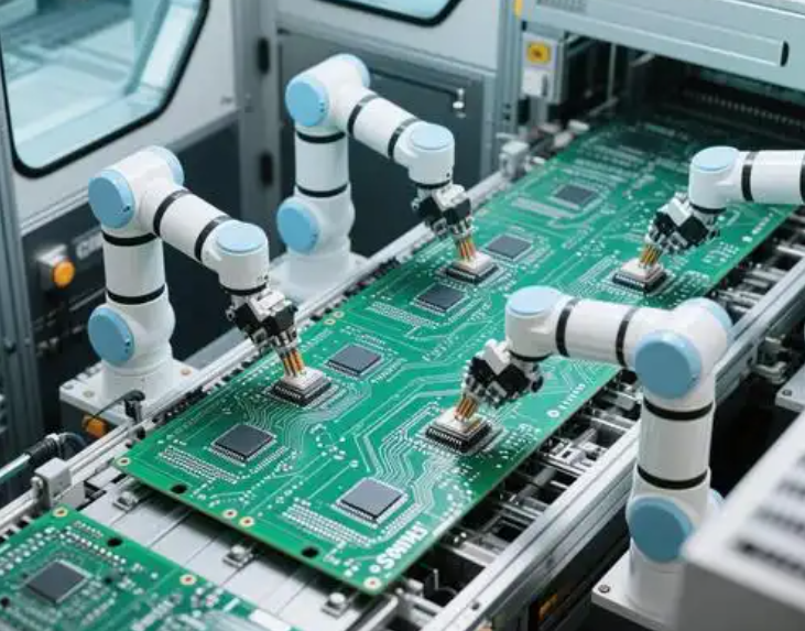
13. Assembly (If Required)
If the project includes assembly, components are mounted using:
- SMT (Surface Mount Technology)
- THT (Through-Hole Technology)
- Mixed technology processes
Industrial assemblies may require additional reinforcement for heavy components or connectors.
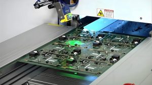
14. Functional Testing and Quality Inspection
The final stage includes:
- Automated optical inspection (AOI)
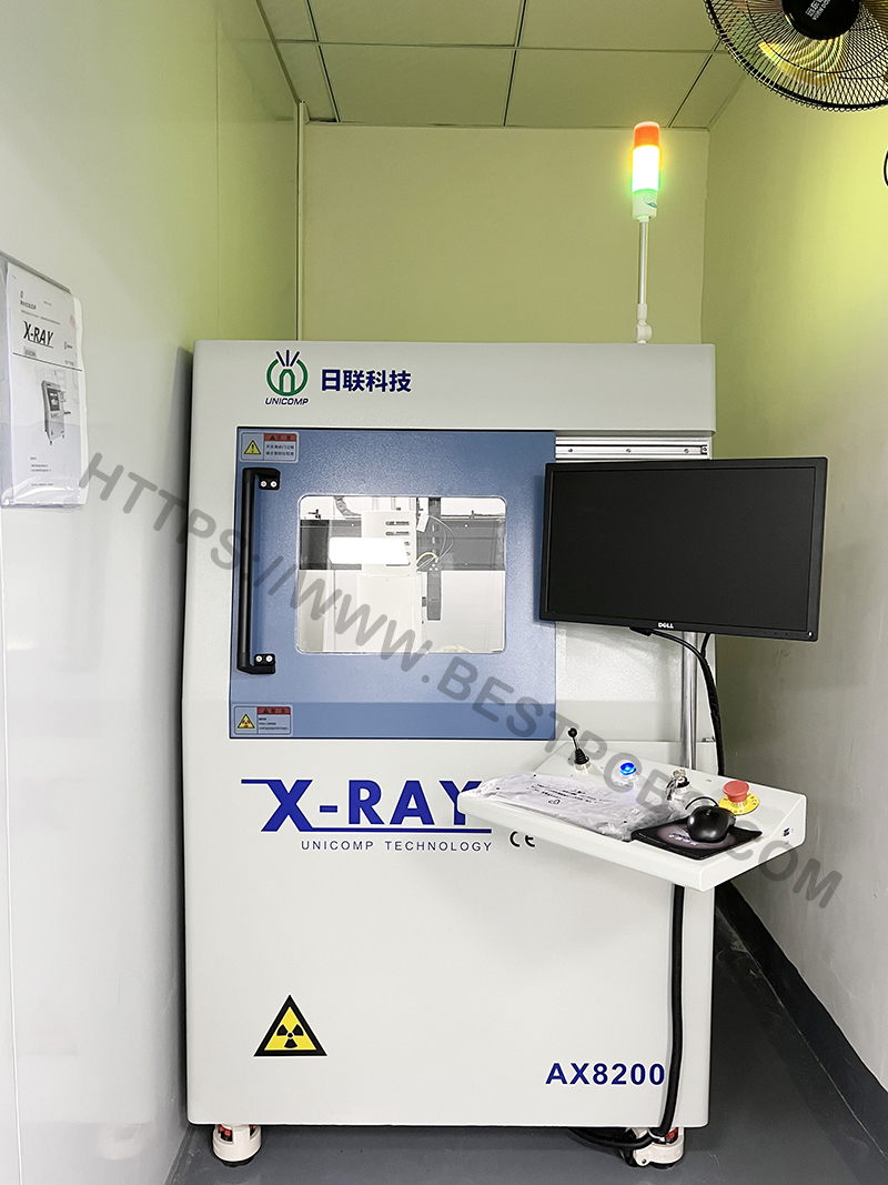
- X-ray inspection for hidden joints
- Functional testing
- Burn-in testing when required
These tests confirm that the board performs under real operating conditions.
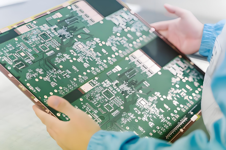
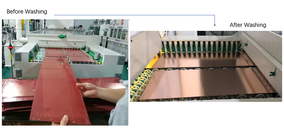
15. Final Inspection and Packaging
Before shipment, boards are visually inspected and cleaned. Moisture-sensitive boards are vacuum sealed with desiccant if required.
Protective packaging prevents mechanical damage during transport, especially for heavy copper or thick boards.
How Much Does Industrial PCB Manufacturing Cost?
Cost depends on several factors:
- Layer count
- Copper weight
- Board size
- Special materials
- Surface finish
- Volume
- Testing requirements
Here is a simplified comparison:
| Feature | Standard PCB | Industrial PCB |
| Copper Weight | 1oz | 2–6oz |
| Material Grade | Standard FR-4 | High-Tg / Polyimide |
| Testing Level | Basic | Extensive |
| Reliability Target | Short to medium term | Long-term operation |
Industrial boards are priced higher because they require premium materials, heavier copper, additional inspection, and longer validation.
However, higher initial cost reduces field failure risks and service interruptions. Over product lifetime, total cost of ownership is lower. Best Technology provides transparent quotations with detailed cost breakdowns to help customers plan effectively.
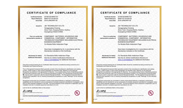
What Certifications Should Industrial PCB Factories Have?
Certifications reflect manufacturing discipline and quality systems.
Key certifications include:
- ISO 9001 – Quality Management
- ISO 14001 – Environmental Management
- UL Certification – Safety compliance
- IPC-A-600 – PCB acceptability
- IPC-A-610 – Assembly standard
- RoHS Compliance
For specialized sectors:
- ISO 13485 for medical
- IATF 16949 for automotive
A certified factory demonstrates structured process control and traceability. Best Technology maintains globally recognized certifications to support industrial customers.
Why Choose EBest As Your Industrial PCB Manufacturing Partner?
Choosing the right manufacturing partner plays an important role in the success of industrial electronics projects. Reliable quality, responsive engineering support, and stable delivery schedules help ensure that products move smoothly from development to production.
At EBest Circuit (Best Technology), we focus on PCB fabrication and PCBA assembly for industrial electronics. Our team supports applications such as automation equipment, power control systems, robotics platforms, and industrial monitoring devices.
Our core manufacturing capabilities include:
- PCB fabrication from 2 to 50 layers
- Support for HDI, heavy copper, and high-frequency PCBs
- Integrated component sourcing and SMT assembly
- Advanced inspection equipment including SPI, AOI, and X-ray systems
- Flexible support for prototype, small batch, and mass production
If you are developing industrial electronics and need reliable PCB fabrication or PCBA assembly support, our engineering team is ready to assist with your project. For technical consultation or a quotation, please contact us at sales@bestpcbs.com.
FAQ
1. What is an industrial PCB?
An industrial PCB is a circuit board designed for equipment operating in demanding environments such as factories, automation systems, and power electronics.
2. What thickness is typical for industrial PCBs?
Common thickness ranges from 1.6 mm to 2.4 mm depending on mechanical requirements.
3. What copper weight is used in industrial PCBs?
Many industrial boards use 2 oz to 6 oz copper layers for higher current handling.
4. What certifications should industrial PCB manufacturers have?
ISO9001, ISO13485, IATF16949, and AS9100 are commonly required for high reliability manufacturing.
5. How do industrial PCBs resist vibration?
Designers increase board thickness, improve mounting structures, and reinforce solder joints.
6. How are industrial PCBs tested?
Manufacturers typically perform AOI inspection, electrical testing, and functional testing before shipment.