IMS PCB vs ceramic substrate is not simply a contest between a low-cost board and a high-performance material. The right choice depends on where heat is generated, how it leaves the assembly, the required electrical isolation, the mechanical environment, and the cost of changing the surrounding design. This guide focuses on those practical consequences so you can identify the better starting point without paying for performance your product cannot use—or accepting risks that appear only after testing.
EBest Circuit supports both IMS PCB and ceramic substrate projects, allowing the discussion to begin with your application rather than a predetermined material. If you are comparing the two for a new design or a redesign, send your operating conditions and current construction to sales@bestpcbs.com. Our team can help you identify which option deserves deeper thermal, electrical, and mechanical validation.
IMS PCB vs Ceramic Substrate: A Quick Comparison
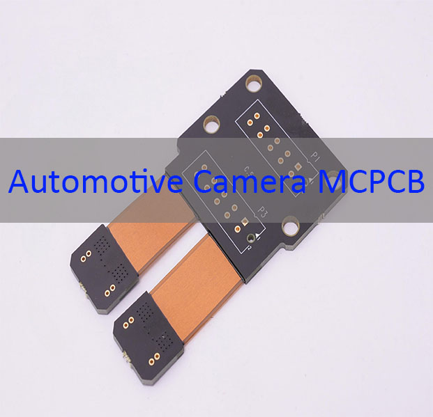
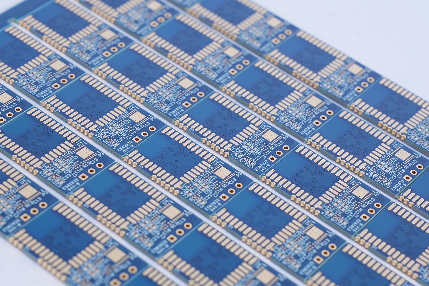
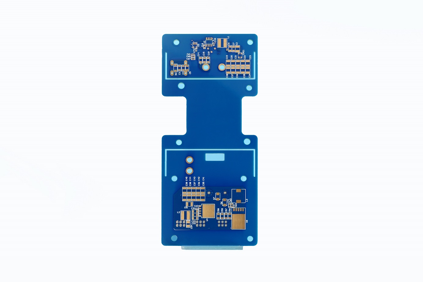
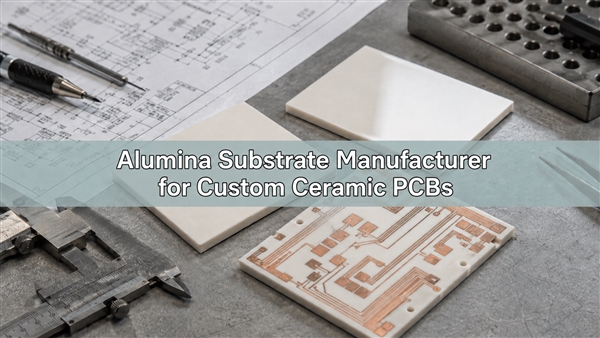
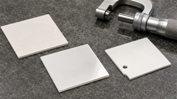
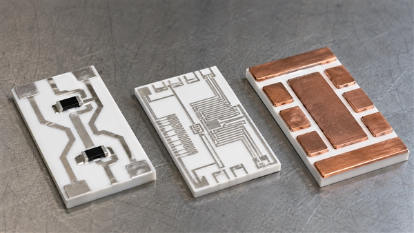
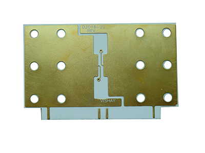
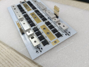
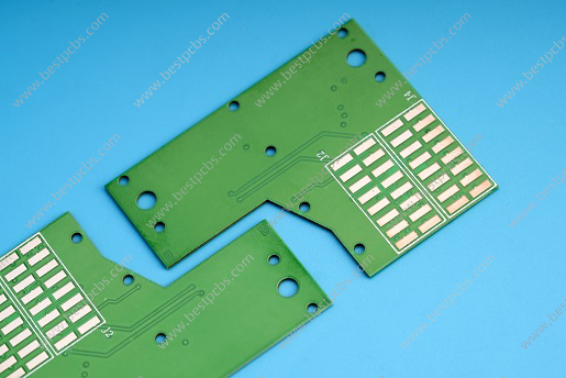
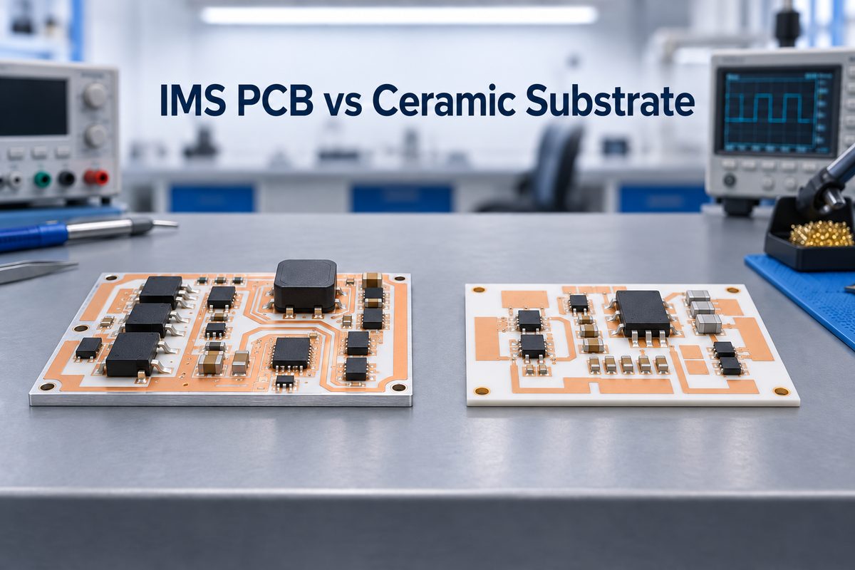
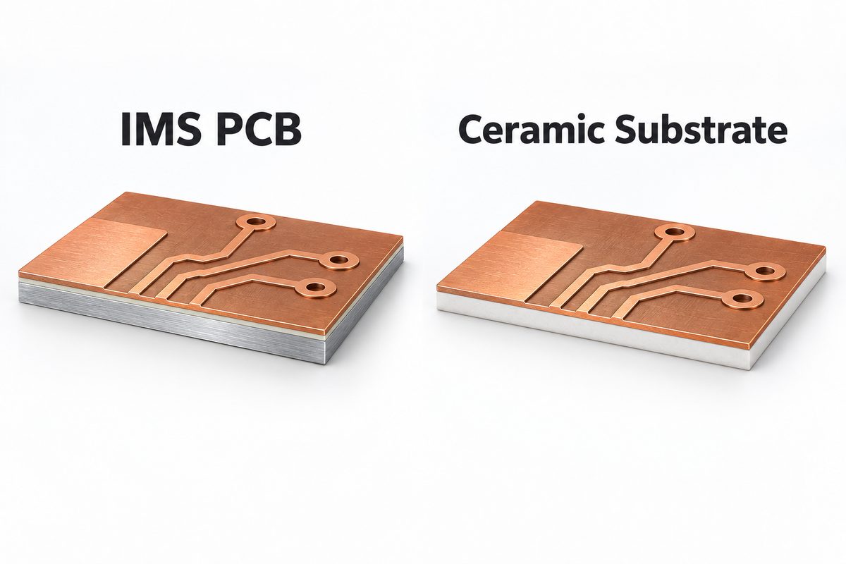
An IMS PCB normally combines a copper circuit, a thermally conductive but electrically insulating dielectric, and an aluminum or copper base. A ceramic substrate uses a ceramic body—commonly alumina or aluminum nitride—as the insulating and heat-conducting foundation. Depending on the ceramic technology, conductors may be formed by thick film, thin film, DPC, DBC, AMB, or another metallization process.
The practical difference is that an IMS PCB moves heat through a thin polymer-based dielectric into a metal plate, while a ceramic substrate can provide insulation and heat transfer through the ceramic itself.
| Your priority | Likely starting point |
|---|---|
| Broad heat spreading at controlled cost | IMS PCB |
| High heat flux in a compact area | Ceramic substrate |
| Resistance to vibration and handling | IMS PCB |
| High-temperature electrical stability | Ceramic substrate |
| Large board area or higher volume | IMS PCB |
| Compact power-device packaging | Ceramic substrate |
This table is a starting point, not a final verdict. A well-designed IMS PCB can outperform an unsuitable ceramic construction at the system level, while ceramic may solve limitations that cannot be corrected by simply changing the IMS dielectric.
When Is an IMS PCB Enough—and When Should You Use a Ceramic Substrate?
An IMS PCB is often enough when the heat source is spread over a reasonable area, the metal base can connect efficiently to a heatsink or housing, and the required isolation can be achieved with a suitable dielectric. This is why IMS is widely considered for LED lighting, power conversion, automotive electronics, motor controls, and other products that need better heat removal than conventional FR-4 without moving to a ceramic platform.
Ceramic becomes more compelling when several demanding conditions occur together:
- Heat is concentrated in a small footprint.
- The assembly operates at elevated temperature.
- High voltage and limited spacing reduce insulation margin.
- Low thermal expansion or dimensional stability is important.
- The substrate is part of a compact power module rather than a large standalone board.
The decision should not be based on power alone. A 100 W load distributed across a large IMS board is different from the same power concentrated under a small semiconductor. Heat-flux density, contact area, cooling method, voltage, and mechanical support are usually more informative than total wattage.
Ceramic should therefore be selected because it removes a known limitation—not simply because its material data sheet contains a higher thermal-conductivity number.
Will a Ceramic Substrate Actually Reduce Your Device Temperature?
It can, but only when the substrate is a meaningful part of the thermal bottleneck.
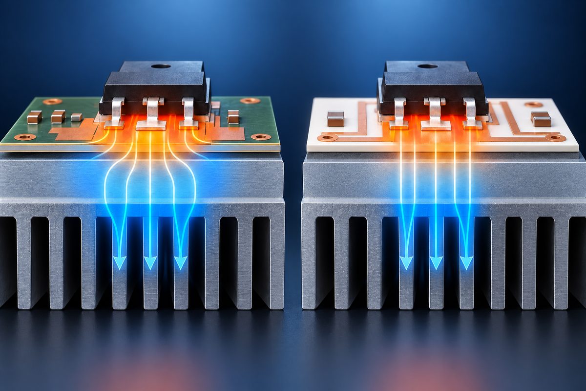
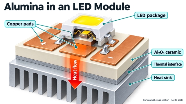
In an IMS PCB, heat typically travels from the component into the copper, through the dielectric, into the metal base, and then through a thermal interface material to a heatsink or housing. The dielectric is thin, but its thermal conductivity is much lower than that of the surrounding copper and metal. When this layer dominates the thermal resistance, moving to an appropriate ceramic substrate may reduce the temperature rise.
However, changing the substrate may provide little benefit if the main restriction is elsewhere. Common examples include:
- A poor component-to-pad thermal connection
- Insufficient copper area around the heat source
- A thick or poorly applied thermal interface material
- An undersized heatsink
- Limited airflow around the enclosure
- High thermal resistance inside the semiconductor package
This is why comparing only material conductivity can be misleading. The useful comparison is the total junction-to-ambient thermal path under the same power, mounting pressure, cooling method, and available area.
Before changing materials, identify where the largest temperature drop occurs. If it is across the IMS dielectric, ceramic may offer a meaningful improvement. If it is between the metal base and the heatsink, improving that interface may deliver a larger result with less redesign.
Do You Need a Ceramic Substrate for Electrical Insulation?
Not every high-voltage design requires ceramic. An IMS PCB can provide electrical isolation when its dielectric material, thickness, conductor spacing, operating temperature, and manufacturing quality are appropriate for the application.
Ceramic becomes more attractive when the design needs insulation performance to remain stable under a combination of high voltage, high temperature, small dimensions, or long service life. Unlike an IMS construction, ceramic does not depend on a thin polymer dielectric between the copper and metal base. That structural difference can provide useful insulation and thermal advantages in demanding power-electronics environments.
The voltage printed on a material data sheet is not a complete design limit. Actual insulation performance is also affected by:
- Dielectric or ceramic thickness
- Conductor geometry and edge spacing
- Surface contamination and humidity
- Voids, cracks, or metallization defects
- Repeated thermal and electrical stress
- Creepage and clearance elsewhere in the assembly
If an IMS PCB already provides adequate isolation margin at the real operating temperature, ceramic may not add enough value to justify a platform change. If the design is losing insulation margin as voltage rises and spacing shrinks, ceramic deserves serious evaluation—but it must still be assessed as part of the complete assembly.
IMS PCB vs Ceramic Substrate: Which Handles Thermal Cycling and Stress Better?
Neither option is universally more reliable because they fail in different ways.
The metal base of an IMS PCB provides toughness and resistance to handling, vibration, and impact. This can be valuable in large boards, vehicle-mounted electronics, lighting assemblies, and products fastened directly to a housing. Its polymer dielectric can also accommodate some strain, although repeated temperature changes may stress copper features, solder joints, interfaces, and the bond between layers.
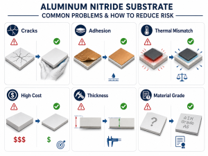
Ceramic offers excellent high-temperature stability and a coefficient of thermal expansion that may better match certain semiconductor materials. This can reduce stress in compact power assemblies. The trade-off is brittleness: unsupported ceramic can crack during machining, assembly, screw fastening, impact, or uneven mounting.
Customers should evaluate reliability against the real environment:
- For vibration, impact, large dimensions, or frequent handling, the mechanical toughness of IMS may be valuable.
- For high operating temperature and close integration with power semiconductors, ceramic may provide better material stability.
- For either option, solder-joint life depends on the expansion mismatch among the substrate, copper, component, solder, and heatsink.
A reliability decision should therefore consider mounting and support conditions alongside the temperature range. Selecting ceramic for thermal reasons while clamping it like a metal board can introduce a new mechanical failure risk.
IMS PCB vs Ceramic Substrate: How Will Each Affect Layout and Assembly?
Changing the substrate can change more than the board material. It may affect routing, conductor formation, component attachment, panel size, mounting, inspection, and the way the finished assembly connects to its cooling structure.
An IMS PCB is often familiar to PCB designers and assemblers. It can support practical board sizes and conventional component assembly, although the metal base and insulation requirements influence drilling, routing, layer structure, and electrical clearances. More complex multilayer IMS constructions are possible, but they should not be treated as equivalent to standard multilayer FR-4.
Ceramic substrates can support compact, thermally demanding circuits and precise conductor technologies, but the selected ceramic process matters. Thick film, thin film, DPC, DBC, and AMB do not offer identical conductor thickness, feature size, bonding method, or cost. The word “ceramic” alone is not enough to define the design rules.
For the customer, the important issue is how far the material change spreads into the rest of the product. IMS usually fits more naturally into familiar PCB routing and solder-assembly workflows, especially when the circuit occupies a larger area. Moving to ceramic may allow a more compact power section, but the available conductor technology can change trace geometry, copper capability, component attachment, and panel utilization.
The mechanical design may change as well. An IMS board can often be fastened to a housing in a familiar way, while ceramic needs even support and controlled mounting pressure to reduce crack risk. The cooling interface must suit the new substrate rather than simply copying the previous stack. A platform change is worthwhile only when these layout and assembly changes produce a clear thermal, electrical, packaging, or reliability benefit in the finished product.
IMS PCB vs Ceramic Substrate Price: What Changes from Prototype to Production?
IMS PCB is usually the more economical starting point for larger boards and volume production because aluminum-base materials and familiar PCB processes are widely available. Ceramic substrates often cost more because the ceramic material, metallization, processing, dimensional control, and handling requirements can be more demanding.
But unit price alone can produce the wrong decision. A ceramic substrate may justify its cost when it enables a smaller power stage, removes a separate insulation component, creates enough temperature margin to avoid a larger cooling system, or supports longer service life at elevated temperature. In those cases, the substrate costs more but the complete product may become smaller, simpler, or more dependable.
Conversely, ceramic is difficult to justify when the product still requires the same large heatsink, enclosure, and board area while gaining little measurable improvement in temperature, insulation margin, or service life.
Prototype pricing can also exaggerate the difference. Small ceramic quantities may carry high setup and process costs, while production economics depend on substrate utilization, conductor technology, yield, inspection, and required tolerances. The useful question is not “Which board is cheaper?” but “Which complete product reaches the required performance and reliability at the lower total cost?”
IMS PCB vs Ceramic Substrate in Three Real Applications
The better option becomes clearer when the comparison is tied to a product rather than an isolated material property.
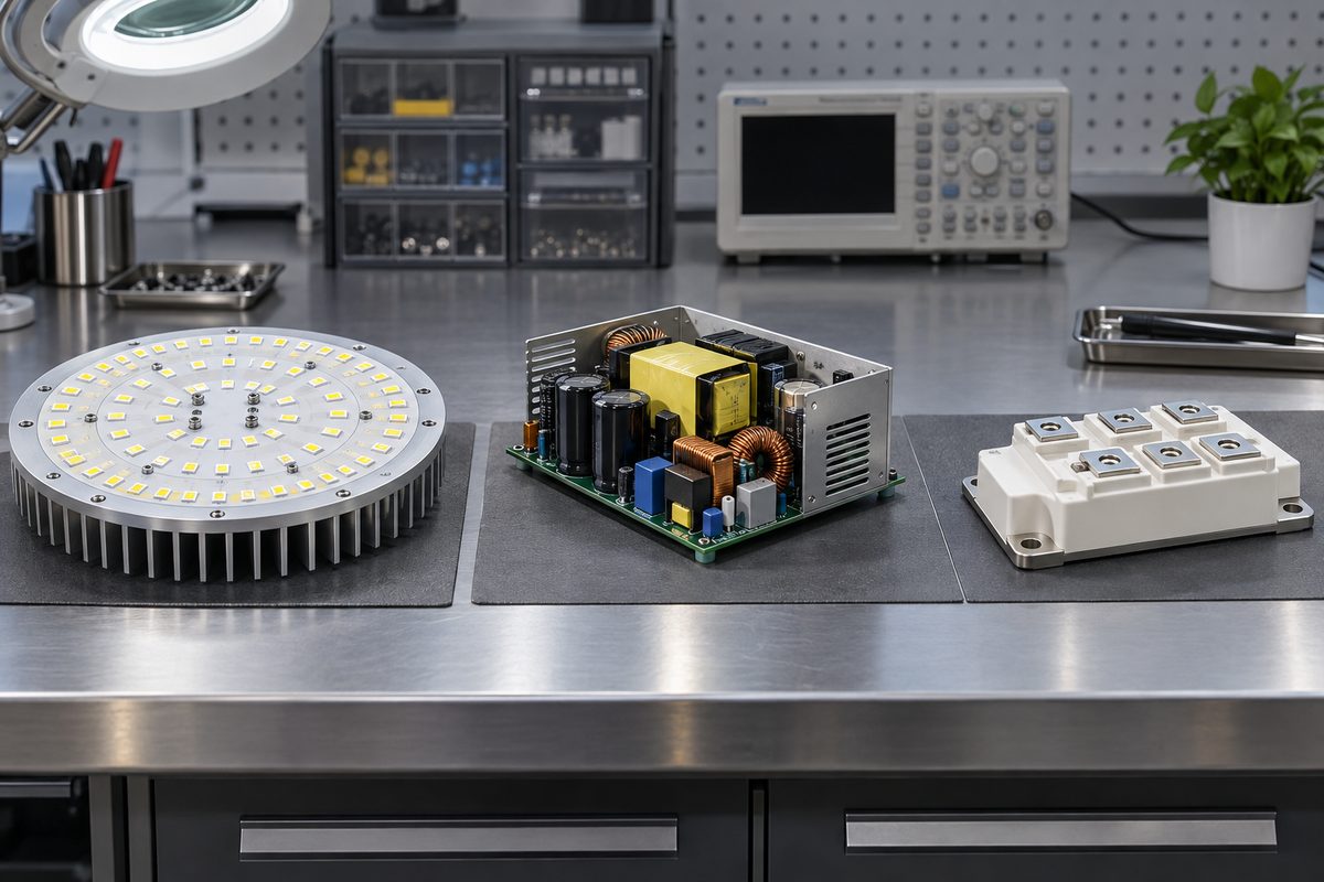
Application 1: Large LED lighting board
The heat sources are distributed across a relatively large area, the board attaches to an aluminum housing, and cost matters at production volume. An aluminum IMS PCB is usually the stronger starting point because it spreads heat, provides mechanical support, and integrates well with conventional LED assembly. Ceramic may not reduce LED temperature enough to offset the additional cost and fragility.
Application 2: Compact high-voltage power converter
The design combines concentrated heat, limited space, high voltage, and elevated operating temperature. A ceramic substrate becomes more attractive because thermal transfer and insulation can be provided within a compact structure. The conclusion still depends on package resistance, conductor requirements, creepage, cooling, and attachment method, but ceramic is more likely to solve a real design constraint here.
Application 3: Vehicle-mounted power electronics
The assembly experiences vibration, temperature cycling, mechanical fastening, and a demanding service life. IMS may be preferred when board area is moderate and mechanical toughness is critical. Ceramic may be selected for a compact power stage with high heat flux, but it needs suitable support and stress-controlled mounting. A hybrid architecture can also be sensible: ceramic for the high-density power section and IMS or another PCB technology for the broader circuit.
These scenarios show why application context matters. The same designer may reasonably select IMS for one product and ceramic for another without contradicting any material specification.
FAQs About IMS PCB vs Ceramic Substrate
Is a ceramic substrate always better than an IMS PCB?
No. Ceramic can provide stronger high-temperature, insulation, and localized thermal performance, but IMS often offers better mechanical toughness, larger practical board formats, familiar assembly, and lower production cost.
Can IMS PCB handle high-power components?
Yes, when the component footprint, dielectric, copper distribution, metal base, interface material, and cooling system create an acceptable total thermal path. Total power alone does not determine suitability.
Does aluminum nitride always outperform alumina?
Aluminum nitride generally offers higher thermal conductivity, but alumina may be adequate and more economical. Metallization, substrate thickness, geometry, interfaces, and the full cooling path still affect the result.
Can ceramic substrate replace an IMS PCB without changing the layout?
Not always. The conductor technology, design rules, substrate size, attachment process, mounting method, and thermal interface may require layout or mechanical changes.
What is the biggest risk when choosing between them?
The biggest risk is optimizing one material property while ignoring the complete product. A higher thermal-conductivity substrate cannot correct every package, interface, heatsink, insulation, or mechanical problem.
How should I compare the two for my project?
Begin with the problem the present design must solve. If the limitation is broad heat spreading, mechanical support, or production cost, IMS is often the logical baseline. If the limitation is concentrated heat, shrinking insulation margin, high operating temperature, or compact power packaging, ceramic deserves closer evaluation. The comparison becomes meaningful when it predicts a product-level result such as lower device temperature, more insulation margin, a smaller assembly, or longer service life.
If you are still deciding about IMS PCB vs ceramic substrate, describe the performance limit you are trying to overcome to sales@bestpcbs.com. EBest Circuit can help you compare realistic constructions and determine whether changing the substrate is likely to improve the finished product before you commit to a prototype.