power divider vs power splitter is a common search when an RF buyer needs to understand whether a circuit only has to distribute signal power or whether it also needs port isolation, balance, controlled impedance, and stable RF performance on the finished PCB.
In real RF projects, the answer is not only a vocabulary difference. The choice affects the circuit topology, expected insertion loss, port-to-port isolation, amplitude balance, phase balance, stackup, laminate choice, copper geometry, connector launch, and the information a PCB manufacturer needs before fabrication.
EBest Circuit does not sell standalone RF power divider or power splitter components. Our role is different: we support RF and high-frequency PCB fabrication, controlled impedance review, material selection review, ENIG and other PCB finishes, and SMT assembly when the customer releases a manufacturable PCB design for production.
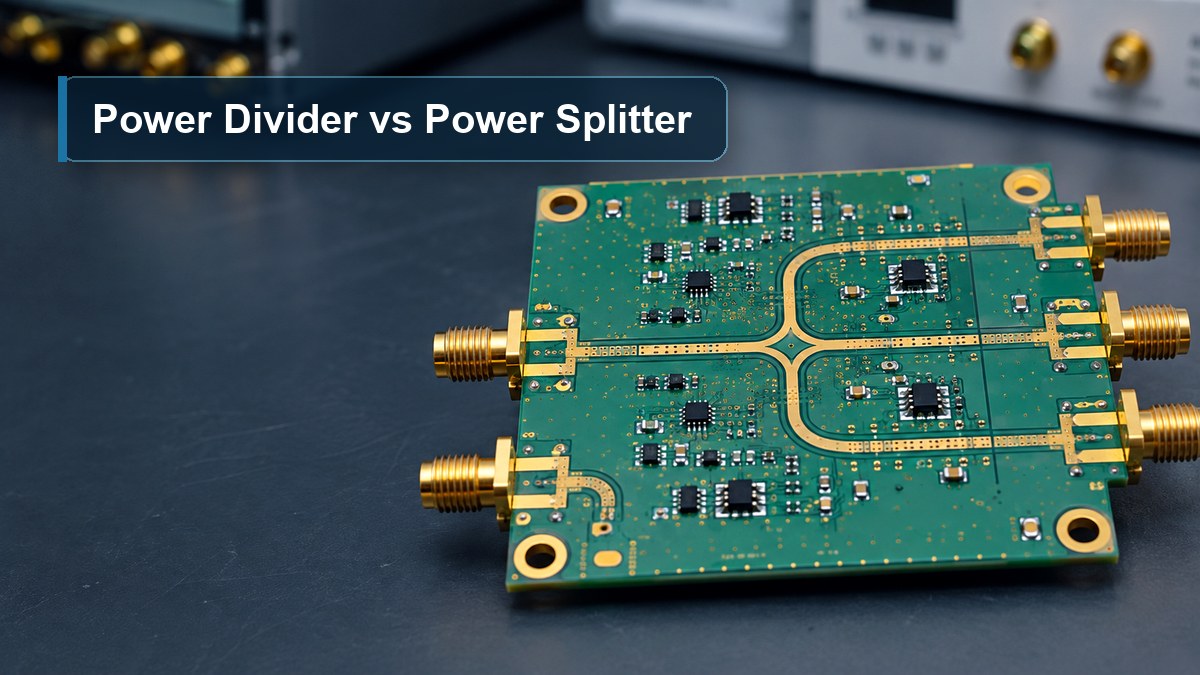
Are Power Dividers and Power Splitters the Same?
Power dividers and power splitters are often used as if they mean the same thing, especially when people are simply describing one RF input being divided into two or more outputs. In many purchasing conversations, that wording overlap is normal.
For engineering work, the distinction matters. A power splitter usually means a simpler signal-splitting network. It may divide power, but it may not provide strong isolation between output ports. A power divider is often expected to provide better impedance matching, defined insertion loss, and isolation behavior, depending on the topology.
For a buyer, the useful question is not “Which word is technically perfect?” The useful question is “What does this RF circuit need the finished PCB to maintain?” If the circuit is only distributing a low-risk signal, a splitter-style structure may be enough. If the circuit must keep two RF paths balanced and isolated, the PCB has to support the divider requirements more carefully.
| Buyer Situation | Usually Acceptable | Reason |
| Simple signal distribution | Power splitter | Lower isolation demand |
| Matched RF outputs | Power divider | Better balance control |
| Two outputs affect each other | Power divider | Isolation becomes important |
| Measured RF performance required | Power divider | Loss, phase, and match must be controlled |
Power Divider vs Power Splitter: Key Differences in RF Circuits
The main difference is how much RF behavior must be controlled after the signal is divided. A splitter can be enough when the application only needs to send one signal to multiple paths and the load interaction is not critical. A divider is more suitable when the outputs must remain matched, isolated, and predictable.
Insertion loss is one of the first differences buyers notice. Any two-way split has theoretical power division loss of about 3 dB before real-world losses are added. The PCB, connectors, copper, dielectric material, solder mask, and assembly can add more loss. For higher-frequency projects, those extra losses become easier to see in test results.
Isolation is another important difference. If one output port reflects energy or changes load condition, poor isolation can allow that change to disturb another output. In a divider circuit designed for isolation, the topology and PCB implementation work together to reduce that interaction.
Amplitude and phase balance also matter. In many RF systems, the two outputs are not judged only by whether signal appears at both ports. They are judged by how closely the two paths match. Small differences in trace width, dielectric thickness, connector launch geometry, via transitions, or electrical length can create measurable differences between outputs.
| RF Requirement | Why Buyers Care |
| Insertion loss | Output signal strength |
| Isolation | Less port interaction |
| Return loss | Better impedance match |
| Amplitude balance | Matched output levels |
| Phase balance | Matched signal timing |
| VSWR | Lower reflected energy |
Power Divider vs Splitter Selection by RF Application
Application context decides whether a splitter is enough or a divider is safer. A lab test fixture, a monitoring point, or a simple distribution path may tolerate a basic splitter. A phased-array, antenna feed, RF front-end, test instrument, telecom module, or microwave signal path usually needs a divider structure with more controlled performance.
For buyers, the selection should start from the performance risk. If two outputs must be nearly equal, the board must protect symmetry. If one output load can change, isolation becomes more important. If the frequency is high enough that small geometry changes affect the result, the PCB stackup and controlled impedance notes must be treated as part of the RF design, not as a general fabrication detail.
| Application Need | Better Direction | PCB Impact |
| Basic signal split | Splitter | Standard RF routing may be enough |
| Equal two-way output | Divider | Matched branch geometry |
| Port isolation needed | Divider | Topology and layout must support isolation |
| High-frequency path | Divider or controlled splitter | Material, impedance, and launch details matter |
| Measured RF board | Divider | Coupons, reports, and tolerances may be required |
This is why an RF PCB buyer should send more than Gerber files when requesting fabrication. Stackup, material, impedance targets, copper weight, solder mask preference, connector type, and test requirements help the manufacturer understand what must be controlled before production starts.
RF Power Divider vs Splitter Parameters That Change PCB Requirements
The RF parameters decide how sensitive the PCB will be. A low-frequency or low-risk splitter may be forgiving. A divider used in a measured RF path is much less forgiving because the board structure becomes part of the circuit.
Frequency is the first driver. As frequency rises, dielectric thickness, Dk stability, copper roughness, trace width, via geometry, and connector launch shape become more important. A small change that does not matter on a simple digital board can change RF behavior on a divider or splitter board.
Power level also matters. Higher power may require wider conductors, thermal consideration, copper thickness review, and spacing checks. If the board is used in a compact RF module, heat, insertion loss, and connector placement may all affect the final build.
Port count changes manufacturing sensitivity. A two-way structure is easier to keep symmetrical than a four-way or eight-way structure. More branches mean more chances for small geometry differences to affect amplitude balance or phase balance.
| Parameter | PCB Detail Affected |
| Frequency | Laminate, Dk, trace geometry |
| Power level | Copper, spacing, heat |
| Port count | Symmetry and branch matching |
| Isolation target | Topology-sensitive layout |
| Phase balance | Electrical length control |
| Connector type | Launch geometry and grounding |
Before quotation, buyers should share the released stackup, controlled-impedance notes, material requirement, copper requirement, surface finish, connector type, and any impedance test or RF test expectation. This allows the manufacturing review to focus on the details that can actually affect the finished board.
RF PCB Material Choices for Divider and Splitter
Material choice affects loss, impedance stability, and repeatability. FR-4 may be acceptable for lower-frequency or less sensitive splitter applications. For higher-frequency divider or splitter circuits, RF laminates such as Rogers, Taconic, Isola, or Shengyi high-frequency materials may be considered depending on frequency, loss target, cost, and availability.
The material decision should be made by the customer’s RF design team. From the manufacturing side, EBest Circuit can review whether the selected material, Dk, dielectric thickness, copper, finished thickness, and surface finish are clearly defined for production.
For divider and splitter PCBs, laminate consistency matters because the signal path is not only a copper trace on a board. The dielectric under or around the trace is part of the transmission-line structure. If the Dk, dielectric thickness, or copper geometry changes, the impedance and electrical length can change with it.
| Material Factor | Buyer Impact |
| Dk stability | More predictable impedance |
| Df / loss tangent | Lower RF loss |
| Dielectric thickness | Trace width and impedance control |
| Copper type | Loss and etching result |
| Pressed stackup | Repeatability across builds |
| Surface finish | Solderability and RF interface reliability |
EBest Circuit can support RF/high-frequency PCB projects using materials such as Rogers, Taconic, Isola, Shengyi, Arlon, and similar laminate systems when the project files define the requirement clearly.
Controlled Impedance in Divider and Splitter RF PCBs
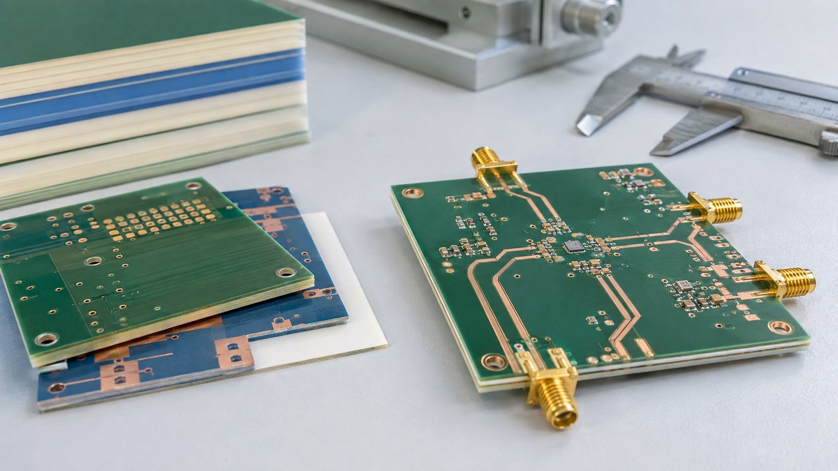
Controlled impedance in a divider or splitter RF PCB does not always mean every RF trace is 50 Ω. The required impedance depends on the circuit topology. In a typical two-way Wilkinson divider, for example, the input and output ports are usually 50 Ω, while the quarter-wave branch lines are about 70.7 Ω.
The most sensitive areas are the input trace, split point, branch lines, output paths, via transitions, and RF connector launches. Even when two output traces look symmetrical, differences in trace width, dielectric thickness, via structure, or electrical length can affect return loss, insertion loss, amplitude balance, and phase balance.
For fabrication, impedance is controlled by finished trace width, copper thickness, dielectric thickness, laminate Dk, transmission-line structure, etching variation, plating result, solder mask condition, and reference-plane continuity.
A common controlled-impedance tolerance is ±10%, while tighter RF designs may specify ±5%, depending on frequency, material system, line geometry, and customer requirements. For a nominal 50 Ω line, ±10% corresponds to approximately 45–55 Ω.
The manufacturing files should identify the controlled traces, target impedance, signal layer, reference plane, material, dielectric thickness, copper thickness, tolerance, and any coupon or test-report requirement. This avoids a common RF PCB problem: the Gerber geometry says one thing, while the stackup or impedance note says another.
EBest Circuit can review the released PCB data to confirm that the stackup, materials, copper, and impedance requirements are clearly defined for fabrication. The RF circuit target remains with the customer’s design team, while our role is to ensure those requirements can be built consistently.
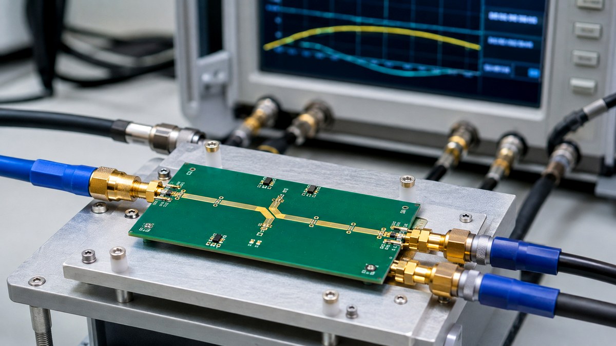
How EBest Circuit Supports RF PCB Builds for Divider and Splitter
EBest Circuit supports divider and splitter PCB projects as RF/high-frequency PCB builds, not as off-the-shelf RF component sales. Buyers provide the released PCB design, stackup, material notes, impedance targets, drawings, and assembly files. We review the manufacturing side before production.
For fabrication, we can review RF laminate selection, finished thickness, copper structure, controlled-impedance requirements, ENIG or other surface finish requirements, solder mask notes, via structures, panelization, and connector-related manufacturing details.
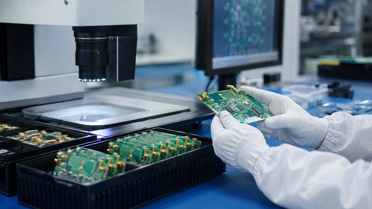
For assembly, EBest Circuit can support SMT and THT requirements when the RF PCB design includes components, SMA connectors, shielding parts, or mixed assembly. The useful result for the buyer is a clearer path from released RF design data to buildable PCB or PCBA production.
| Buyer Sends | EBest Circuit Reviews |
| Gerber and drill files | Fabrication feasibility |
| Stackup drawing | Layer and dielectric consistency |
| Impedance table | Target values and tolerances |
| Material notes | Laminate and copper requirements |
| BOM and CPL | SMT assembly readiness |
| Connector drawings | Launch and footprint clarity |
If files are incomplete, the buyer gets fewer surprises when the open items are clarified before fabrication. If the files are consistent, the project can move into production with less risk of stackup, material, or impedance misunderstanding.
RF PCB Case Study for a Power Divider Project
A two-way RF power divider project submitted to EBest Circuit required controlled-impedance transmission lines and closely matched output paths. The PCB used Shengyi S1000-2 TG170 material, a finished thickness of 1.60 mm ±10%, ENIG surface finish, and a specified 50 Ω trace with a 0.19 mm line width on the inner signal layer.
The divider had one RF input and two outputs. The input and output transmission lines were designed for 50 Ω, while the quarter-wave divider branches used approximately 70.7 Ω impedance. The design also specified an amplitude balance within ±0.3 dB and a phase balance within ±3° between the two outputs. SMA connectors were used for the RF input and output interfaces.
Problem
During the manufacturing review, the specified 50 Ω trace geometry did not fully match the released stackup information. For this power divider, the issue was important because the input, 70.7 Ω branch sections, and two 50 Ω output paths depended on defined transmission-line geometry.
If the board had entered production without clarification, changes in dielectric thickness or finished trace geometry could have shifted the impedance and created differences between the two RF paths, potentially affecting return loss, insertion loss, amplitude balance, and phase balance.
Solution
Before fabrication, EBest Circuit reviewed the laminate, copper structure, dielectric thickness, finished board thickness, 50 Ω traces, and 70.7 Ω branch-line requirements with the customer. The production stackup and impedance parameters were aligned before manufacturing.
The two output paths and SMA launch areas were also reviewed for consistent RF geometry and reference-plane conditions.
The project required turnkey SMT assembly as well. After assembly, each board was carefully cleaned, with no solder balls or other visible contamination allowed on the PCB surface.
Result
The production stackup and controlled-impedance structure were confirmed before fabrication, reducing the risk of impedance deviation between the input, divider branches, and two output paths.
By resolving the manufacturing data before production, the PCB could be built around the intended 50 Ω and 70.7 Ω transmission-line structures while maintaining the geometry required for consistent RF output performance.
FAQs About Power Divider vs Power Splitter
Is a power divider the same as a power splitter?
They are often used interchangeably in casual RF discussions, but a power divider usually implies more defined matching, isolation, and balance behavior. A splitter may simply divide signal power with less isolation.
When is a power splitter enough?
A splitter may be enough for simple signal distribution, lab monitoring, low-risk test paths, or applications where output-to-output interaction is not critical.
When should buyers use a power divider?
A power divider is more suitable when the outputs need controlled matching, isolation, amplitude balance, phase balance, or stable performance across a defined frequency range.
Does every divider or splitter RF PCB use 50 Ω traces?
No. Many RF ports are 50 Ω, but some divider branches may use other impedance values. A two-way Wilkinson divider, for example, commonly uses about 70.7 Ω quarter-wave branch lines.
What PCB information should be provided for a divider or splitter board?
Send Gerber files, drill files, stackup, material requirement, copper thickness, controlled-impedance table, surface finish, connector information, and any impedance coupon or test-report requirement.
Can EBest Circuit design the RF divider or splitter circuit?
The RF circuit design and performance target should come from the customer’s design team. EBest Circuit can review the released files for PCB manufacturability, stackup clarity, material definition, impedance requirements, fabrication, and assembly readiness.
Can EBest Circuit manufacture RF divider and splitter PCBs?
Yes, when the customer provides released manufacturing data. EBest Circuit can support RF/high-frequency PCB fabrication, controlled-impedance review, surface finish, and SMT assembly where required.
If you are comparing power divider vs power splitter requirements for an RF PCB project, send your Gerber files, stackup, impedance notes, material requirement, BOM, CPL, and quantity to sales@bestpcbs.com. EBest Circuit can review whether the released data is clear enough for RF PCB fabrication and assembly before production starts.