Indium phosphide is a key semiconductor material for optical communication, high-speed photonics, infrared detection, and selected RF devices. Demand has also grown with AI data-center infrastructure, where high-speed optical links increasingly rely on InP-based lasers, detectors, and photonic components.
For engineers and buyers, however, choosing an InP substrate is not simply a matter of ordering a 2-inch or 4-inch wafer. Conductivity type, dopant, crystal quality, EPD, orientation, surface condition, and supplier consistency can all affect epitaxial growth and device yield. This guide explains the main types, applications, available sizes, material alternatives, pricing factors, suppliers, and current supply risks.
What Is an Indium Phosphide (InP) Substrate?
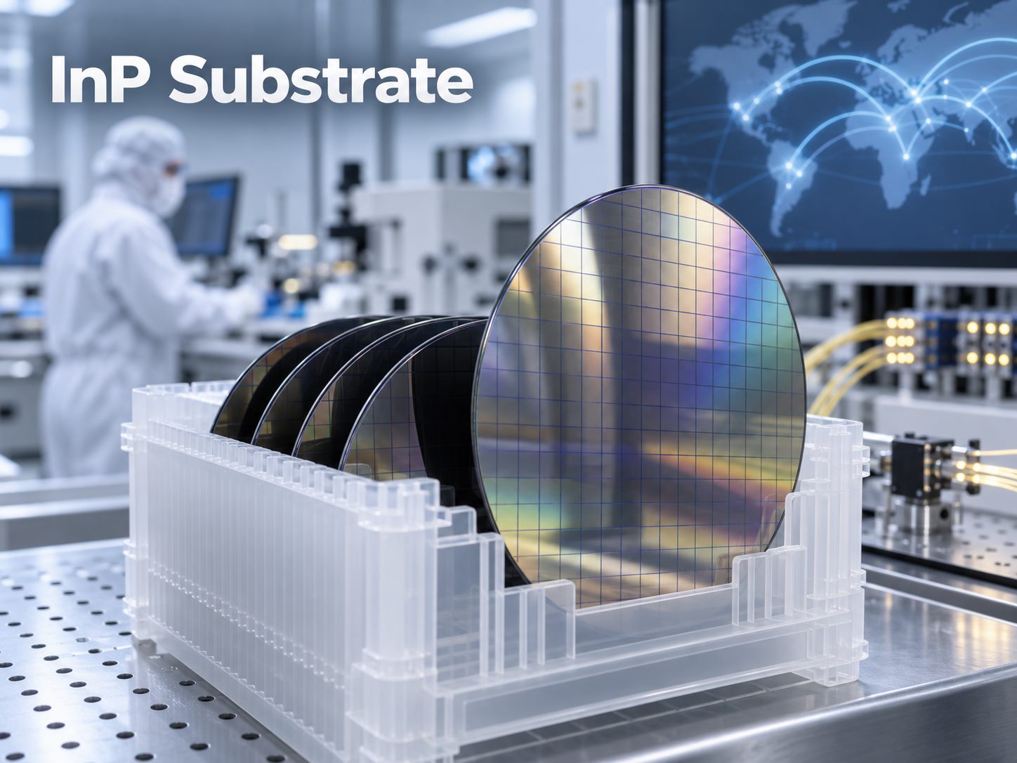
An InP substrate is a single-crystal wafer made from indium phosphide, a III-V compound semiconductor consisting of indium and phosphorus.
It is mainly used as the crystalline foundation on which additional semiconductor layers are grown. Materials such as InGaAs, InGaAsP, and InAlAs can be deposited on InP to form active device structures for lasers, photodetectors, modulators, HBTs, HEMTs, and photonic integrated circuits.
The terms InP wafer and InP substrate are often used interchangeably, but the manufacturing context matters:
- Bare InP substrate: A polished single-crystal wafer before epitaxial growth.
- Epi-ready InP substrate: A polished and cleaned wafer prepared for MOCVD or MBE epitaxy.
- InP epiwafer: An InP substrate with one or more epitaxial semiconductor layers already grown on it.
This distinction matters in sourcing. A company that grows bulk InP crystals and supplies polished substrates is providing a different product from an epitaxy supplier offering a completed device layer structure.
What Is an InP Substrate Used For?
InP substrates are mainly used where the device requires long-wavelength photonics, high-speed optical conversion, infrared detection, or very high-frequency electronic performance.
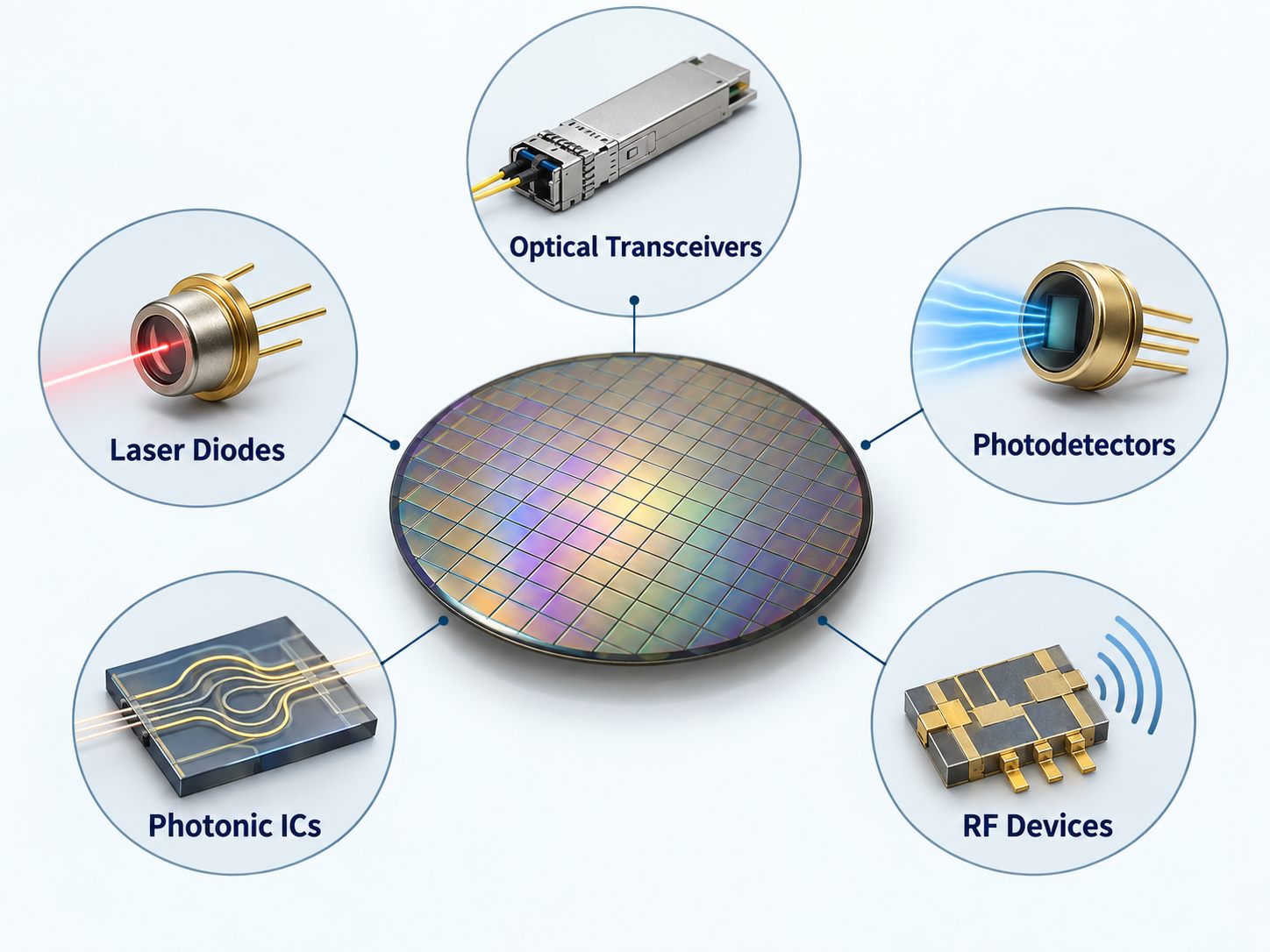
Typical applications include:
- Optical transceivers for telecom networks and data centers
- DFB and FP laser diodes
- Electro-absorption modulated lasers
- PIN photodiodes and avalanche photodiodes
- Photonic integrated circuits
- Optical modulators and amplifiers
- Short-wave infrared detectors
- LiDAR and optical sensing
- HBT and HEMT devices
- Millimeter-wave electronics
One of InP’s strongest application areas is optical communication around 1310 nm and 1550 nm. The substrate supports III-V epitaxial systems such as InGaAsP and InAlGaAs that can be engineered for these telecom wavelength bands.
This makes InP particularly useful in laser sources, detectors, and integrated photonic devices used in high-speed optical links. Silicon photonics may handle routing and passive functions in the same module, but active light generation and detection often still rely on III-V materials.
What Types of InP Substrates Are Available?
InP substrates are usually classified by conductivity type and dopant.
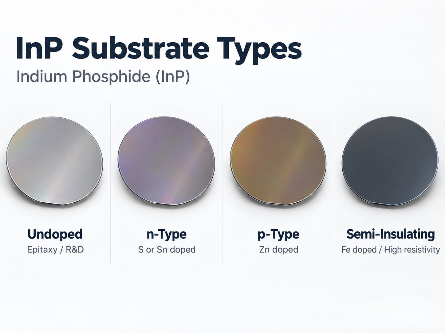
| InP Substrate Type | Common Dopant | Electrical Behavior | Typical Use |
| Undoped InP | None | Usually lightly conductive | Epitaxy, research, special structures |
| n-Type InP | S or Sn | Electron-conducting | Lasers, detectors, optoelectronics |
| p-Type InP | Zn | Hole-conducting | Selected device structures |
| Semi-insulating InP | Fe | Very high resistivity | RF, HBT, HEMT and isolated device structures |
Semi-insulating InP substrate is especially important for high-frequency electronics. Its high resistivity helps limit unwanted current paths through the substrate and improves isolation between active areas.
Specifying only “n-type” or “semi-insulating” is not enough for production purchasing. The RFQ should also define the required:
- Carrier concentration
- Resistivity
- Mobility, where relevant
- Dopant type
- Electrical tolerance range
Two wafers sold under the same general category can still have substantially different electrical characteristics.
What Sizes Are InP Substrates Available In?
Commercial InP substrates are commonly available in 2-inch, 3-inch, and 4-inch diameters, while 6-inch InP is becoming more important for higher-volume manufacturing.
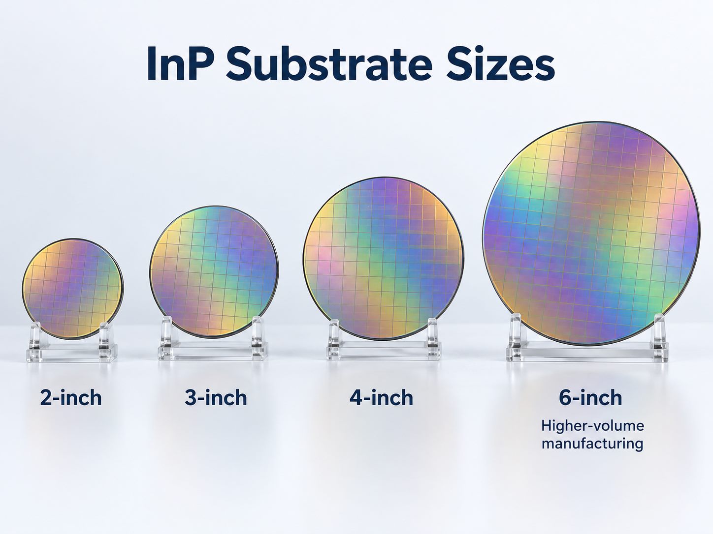
| Nominal Size | Diameter | Typical Use |
| 2 inch | 50.8 mm | R&D, legacy production, specialty devices |
| 3 inch | 76.2 mm | Established compound-semiconductor production |
| 4 inch | 100 mm | Common modern production platform |
| 6 inch | 150 mm | Higher-volume and newer manufacturing platforms |
Availability varies by supplier. A manufacturer that routinely ships 3- or 4-inch material may not have qualified 6-inch capacity.
Larger wafers can improve production economics because more dies are processed in one batch, but scaling InP crystal growth is difficult. Maintaining low EPD, good flatness, uniform electrical properties, and acceptable yield becomes harder as crystal diameter increases.
For that reason, a 6-inch requirement should be discussed with suppliers early. Do not assume it will have the same lead time, grade availability, or supplier base as 4-inch material.
InP vs GaAs vs Silicon: When Should You Use Each Substrate?
InP is not the best substrate for every semiconductor device. It becomes attractive when its material system provides a performance advantage that is difficult to reproduce with GaAs or silicon.
| Selection Factor | InP | GaAs | Silicon |
| 1310/1550 nm photonics | Excellent | Limited | Strong passive platform |
| Native light generation | Excellent | Excellent in suitable wavelengths | Poor |
| High-frequency electronics | Excellent | Excellent | Good |
| Photonic integration | Strong | Application-dependent | Very strong ecosystem |
| Large wafer availability | Limited | Better than InP | Excellent |
| Material cost | High | High | Low |
| Manufacturing scale | Specialized | Mature III-V | Extremely mature |
Use InP when the device architecture depends on:
- InGaAs-based photodetection
- Long-wavelength semiconductor lasers
- High-speed InP HBTs
- Integrated III-V photonics
- Epitaxial structures lattice-matched to InP
GaAs is often more suitable for VCSELs, RF amplifiers, LEDs, and some sensing systems. Silicon remains the preferred choice when low cost, large wafer size, CMOS compatibility, and mature manufacturing are more important than native III-V optical performance.
The material choice should therefore start with device physics rather than wafer price.
How Much Does an InP Substrate Cost?
InP substrate prices vary widely, so there is no reliable single market price.
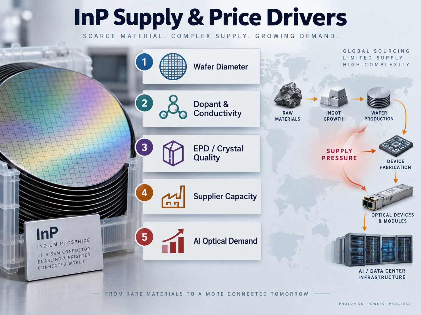
Small research-grade wafers may cost hundreds of dollars, while larger production-grade, low-defect, or epi-ready wafers can reach four-figure prices per wafer. During supply shortages, pricing can rise well beyond normal levels.
An InP substrate price quote should therefore be compared against the complete wafer specification and supply terms. The main price drivers include:
- Wafer diameter
- Conductivity type
- Dopant
- EPD requirement
- Crystal quality
- SSP or DSP polishing
- Epi-ready finishing
- Orientation tolerance
- Flatness requirements
- Inspection level
- Quantity
- Supplier capacity
A quotation issued during a shortage may also reflect capacity allocation rather than normal manufacturing cost.
When comparing InP substrate suppliers, send the same specification to each company. Otherwise, a lower price may simply correspond to a higher EPD, wider geometric tolerance, different polishing grade, or less demanding inspection criteria.
Why Are InP Substrates in Short Supply?
The current shortage is largely the result of fast-growing optical demand meeting a relatively concentrated substrate manufacturing base.
Several factors are involved:
- AI data-center growth: Faster optical interconnects require more lasers, detectors, and optical transceiver components.
- Limited crystal-growth capacity: High-quality InP single-crystal production is difficult to scale quickly.
- Supplier concentration: Only a limited number of companies can manufacture qualified production-grade material at volume.
- Long qualification cycles: Switching substrate suppliers can require new epitaxy, wafer-fab, reliability, and customer validation.
- 6-inch transition: Larger-diameter production requires new crystal-growth capability and downstream qualification.
- Trade restrictions: Export controls and geographic concentration can create regional availability problems.
- Capacity reservation: Large device manufacturers increasingly secure substrate volumes through long-term agreements.
For procurement teams managing InP substrate shortages, the useful response is not simply buying excess inventory. Our overview of critical semiconductor supply-chain materials provides additional context for qualification and continuity planning. Better controls include:
- Qualifying a second source
- Providing suppliers with realistic demand forecasts
- Identifying acceptable alternative grades
- Tracking lead-time changes
- Reserving capacity for production programs
- Requalifying material changes before volume release
Main InP Substrate Companies Globally
The global InP supply chain includes bulk crystal growers, polished substrate manufacturers, epitaxy companies, device fabs, and distributors. They should not be treated as the same type of supplier.
Several established InP substrate companies with documented substrate capabilities include:
| Company | Region | InP Capability | Buyer Should Confirm |
| Sumitomo Electric | Japan | Semi-insulating and conductive InP substrates | Diameter, grade and available capacity |
| JX Advanced Metals | Japan | Multiple diameters and dopant options | EPD, flatness and capacity allocation |
| AXT | USA / global manufacturing | Multiple wafer sizes including large-diameter InP | Origin, qualification and availability |
| Freiberger Compound Materials | Germany | Semiconducting and semi-insulating InP | EPD grade, polish and orientation |
| IQE / Wafer Technology | UK / USA | InP substrate and epi-ready wafer capability | Bare substrate vs epitaxial scope |
This is not a ranking.
A well-known company may still be unsuitable for a specific program if it cannot support the required diameter, dopant, EPD, surface condition, monthly volume, or qualification history.
Buyers should also establish what the company actually controls:
- Bulk crystal growth
- Wafer slicing
- Grinding and polishing
- Epi-ready surface preparation
- Epitaxial growth
- Distribution only
That distinction becomes important when investigating yield problems or controlling future process changes.
How Should You Choose an InP Substrate Supplier?
Start with the released wafer specification rather than the supplier’s standard product catalog.
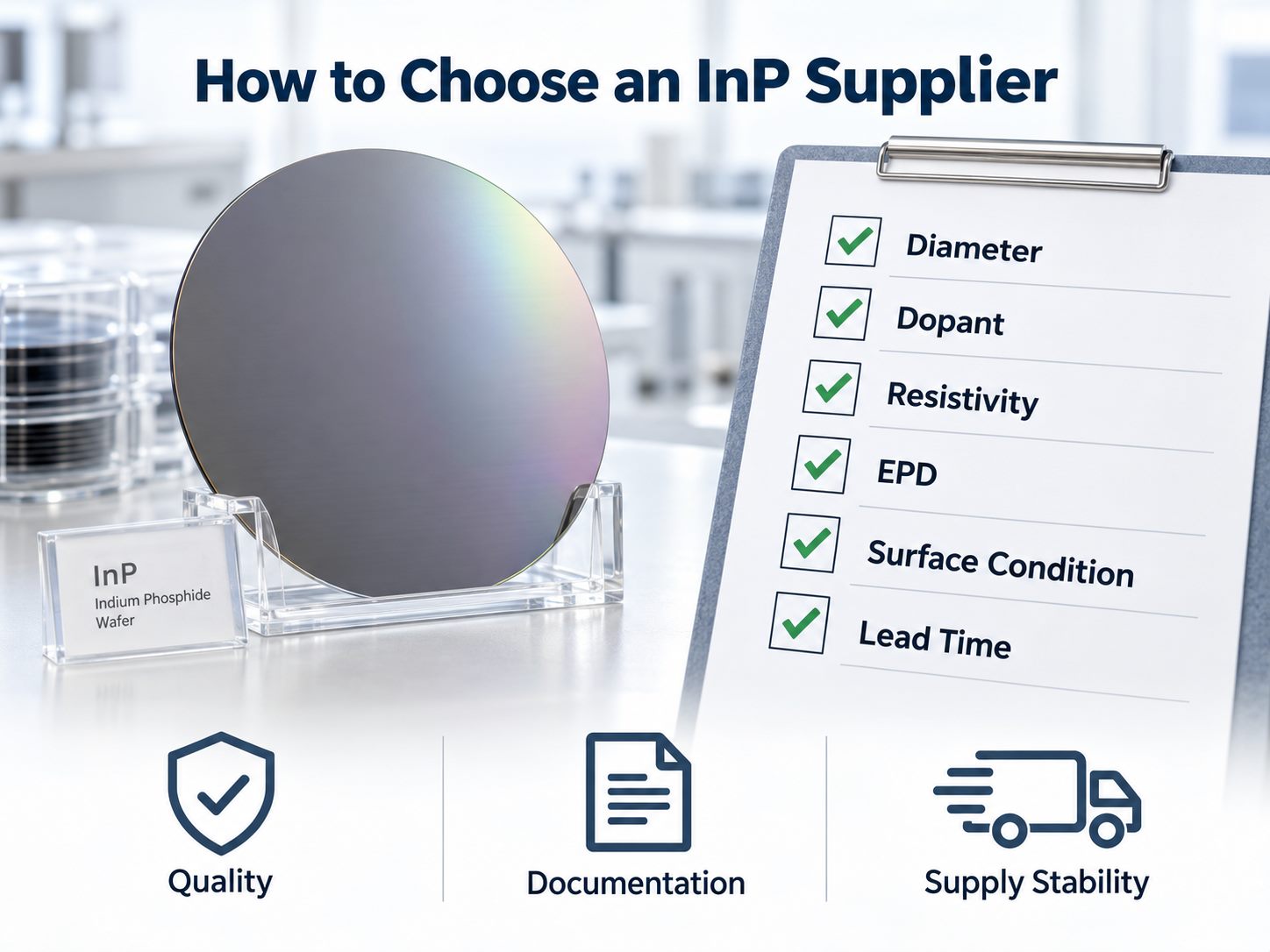
A useful RFQ should include three groups of information.
Material requirements
- Diameter and thickness
- Crystal orientation
- Off-cut, if required
- Conductivity type
- Dopant
- Carrier concentration or resistivity
- Maximum EPD
Geometry and surface requirements
- TTV
- Bow
- Warp
- SSP or DSP
- Surface roughness
- Epi-ready requirement
- Flat or notch
- Particle and contamination limits
Quality and supply requirements
- Certificate of analysis
- Lot traceability
- Electrical test data
- EPD data
- Packaging method
- Standard lead time
- Monthly capacity
- MOQ
- Change-notification policy
For production programs, also confirm how the supplier handles changes to crystal-growth equipment, polishing processes, raw materials, manufacturing locations, or inspection methods.
The lowest wafer price is not always the lowest program cost. Stable epitaxy yield, lot-to-lot consistency, controlled changes, and predictable delivery can be more valuable than a small difference in substrate price.
InP Substrate FAQs
1. What does semi-insulating InP mean?
Semi-insulating InP is engineered to have very high electrical resistivity rather than behaving like a normal conductive n-type or p-type semiconductor substrate. Fe compensation is commonly used. The high-resistivity substrate helps isolate active device regions and reduce parasitic electrical paths, making it useful for HBTs, HEMTs, RF devices, and selected integrated circuits.
2. What dopants are commonly used in InP substrates?
Common InP dopants include sulfur and tin for n-type material, zinc for p-type material, and iron for semi-insulating material. Undoped material is also available. The exact dopant should be specified together with the required carrier concentration or resistivity rather than by dopant name alone.
3. What is an epi-ready InP substrate?
An epi-ready InP substrate has been polished, cleaned, inspected, and packaged so its surface is suitable for epitaxial growth. Important controls may include surface roughness, particles, haze, contamination, orientation, and flatness. Epi-ready should still be defined against the supplier’s specification because the term does not establish one universal surface limit.
4. Why is InP more expensive than silicon?
InP is more expensive because crystal growth is more difficult, usable crystal diameter is smaller, material volume is much lower, defect control is more demanding, and the manufacturing ecosystem is far less scaled than silicon. Silicon benefits from enormous 200 mm and 300 mm production infrastructure that InP does not have.
5. How is InP substrate quality measured?
No single measurement defines InP quality. Typical controls include EPD, resistivity or carrier concentration, mobility, crystal orientation, TTV, bow, warp, surface roughness, particle count, contamination, and visual defects. Which parameter deserves the tightest limit depends on the intended epitaxial structure and device process.
6. Can InP substrates be replaced by GaAs?
Sometimes, but not as a direct drop-in replacement. GaAs can replace InP only when the required device structure, wavelength, lattice-matched epitaxial system, and electrical performance can be redesigned around GaAs. For many 1310/1550 nm lasers, InGaAs detectors, and InP-based high-speed photonic devices, changing to GaAs would require a different epitaxial and device architecture rather than simply changing the substrate.
InP substrates provide capabilities that are difficult to reproduce with silicon or GaAs in specific high-speed photonic and electronic applications, but those advantages come with higher material cost, tighter supplier capacity and more demanding qualification requirements. Before purchasing, define the substrate by its diameter, conductivity, dopant, electrical range, EPD, orientation and surface condition, then compare suppliers on both technical consistency and supply continuity.
If your InP-based optical, RF, or semiconductor device is moving into PCB or PCBA integration, EBest Circuit can review the board-level manufacturing requirements, controlled-impedance interfaces, assembly constraints, and production data. Send your Gerber files, BOM, drawings, and project requirements to sales@bestpcbs.com for engineering review and quotation.