





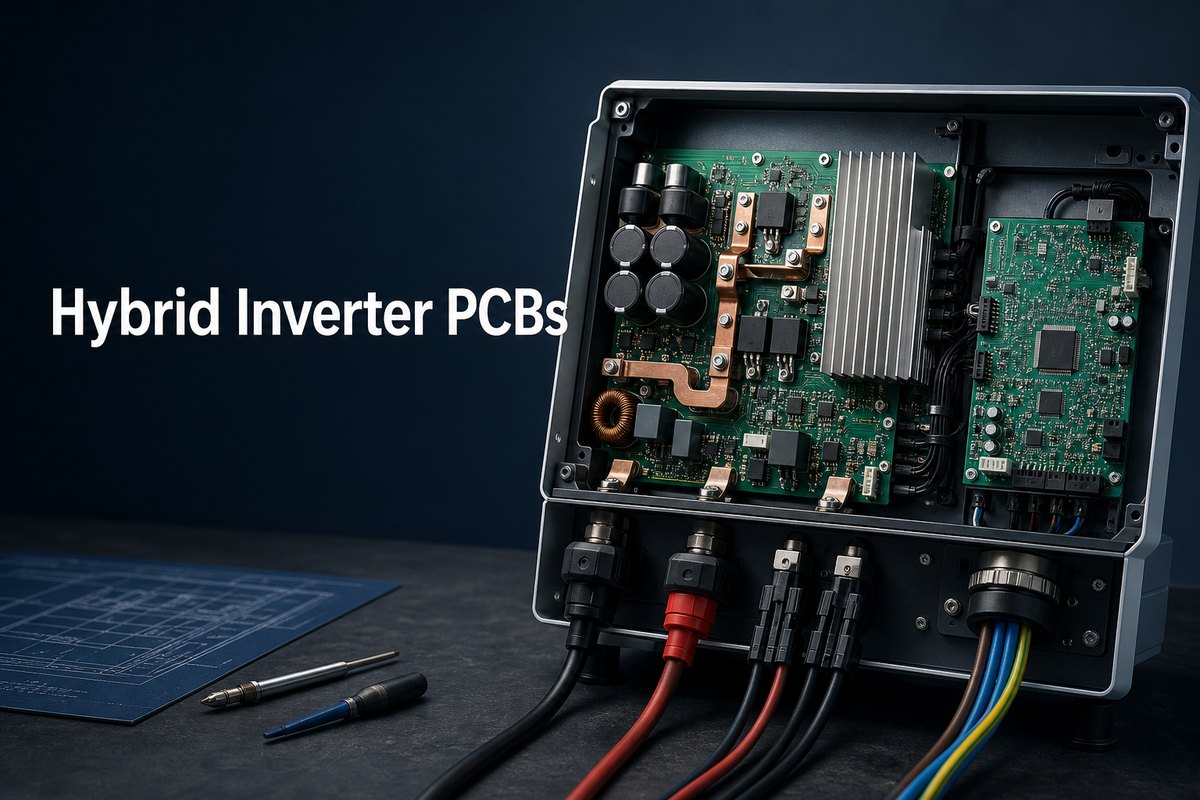
Hybrid Inverter PCBs coordinate more power paths than a conventional grid-tied inverter board. They may receive energy from photovoltaic strings, charge or discharge a battery, form or follow an AC output, communicate with a battery-management system, and protect the product during faults or operating-mode changes. That combination makes board partitioning, insulation, switching-loop control, thermal design, and test access inseparable engineering decisions.
This guide explains how a hybrid inverter PCB is divided into functional blocks, what makes its layout difficult, and which manufacturing information should be settled before prototype release. The focus is the custom PCB and PCBA—not a replacement module selected only by inverter model number.
What Are Hybrid Inverter PCBs?
A hybrid inverter PCB is part of the electronic platform that routes and converts energy among a photovoltaic array, battery, utility grid, and local loads. Unlike a simple DC-to-AC board, it must support multiple operating states: solar generation, battery charging, battery discharge, grid import, grid export where permitted, backup operation, and fault shutdown.
The phrase can refer to one integrated board or a coordinated set of boards. A compact unit may combine control, sensing, gate drive, auxiliary power, and portions of the power stage. Higher-power equipment often separates these functions so that heat, isolation, serviceability, and mechanical current paths can be managed independently.
How Does a Hybrid Inverter PCB Diagram Divide Power and Control?
A useful hybrid inverter pcb diagram begins with energy flow, not with component placement. The PV path normally includes input protection and an MPPT-controlled DC/DC stage. The battery path is often bidirectional because the same product must charge and discharge the battery. Both paths interact through a DC link before the DC/AC stage supplies the grid or protected loads.
Control, sensing, protection, and communications supervise every conversion stage. They measure voltage, current, and temperature; drive power switches; coordinate relays or contactors; communicate with the BMS; and move the system to a defined state when a reading becomes invalid.
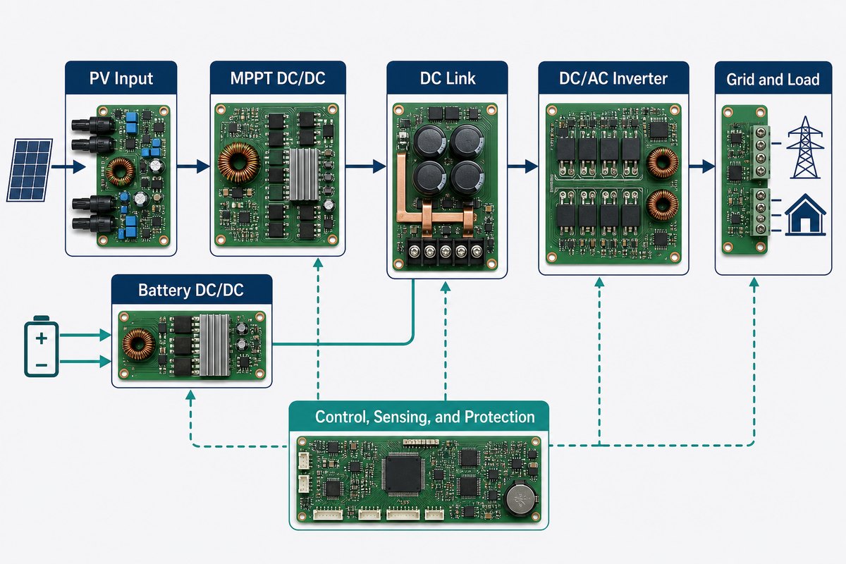
The diagram is an architecture map, not a manufacturing drawing. Before layout, each boundary must identify the maximum working and transient voltages, current direction, isolation requirement, switching frequency, signal bandwidth, fault energy, connector system, and cooling path. These inputs determine which functions can safely share a board.
Which Boards Belong in a Hybrid Inverter?
There is no universal board count. The right split depends on power level, enclosure geometry, service strategy, semiconductor package, cooling method, and certification path. The following division is common enough to guide an early design review.
| Board or Module | Primary Function | Main PCB Concern |
|---|---|---|
| PV / MPPT power board | Conditions photovoltaic input and tracks the operating point | Switching-loop inductance, current path, sensing accuracy, and heat |
| Bidirectional battery board | Controls battery charge and discharge | Current reversal, protection coordination, bus impedance, and BMS interface |
| DC/AC inverter board | Converts the DC-link energy into controlled AC | Gate-drive loops, commutation paths, common-mode noise, and cooling |
| Control and communications board | Runs control algorithms, measurements, protection logic, and communications | Clean references, ADC routing, isolation, return paths, and firmware test access |
| Auxiliary supply / gate-driver board | Provides isolated rails and switch control | Isolation barrier, transformer parasitics, local decoupling, and propagation matching |
| DC-link / filter assembly | Stores energy and filters switching components | Low-inductance interconnect, mechanical fastening, ripple current, and clearance |
A modular split can simplify cooling and replacement, but it adds connectors, harnesses, fastening tolerances, and interface failure points. An integrated hybrid inverter pcb board reduces interconnects, yet it concentrates heat and makes the high-energy and low-level circuits harder to separate. The tradeoff should be decided from electrical and mechanical requirements, not from board area alone.
How Should PV, Battery, DC-Link, and Grid Paths Be Partitioned?
Partition the assembly by energy domain and noise sensitivity. A practical floorplan keeps switching power cells compact while preventing high-dv/dt copper, high-di/dt loops, and hot components from crossing through measurement and communication areas.
- Define current loops first. Mark the commutation loop for each switching stage and place its local capacitors before routing low-level signals.
- Keep the DC link physically close to the power stage. Long bus paths add parasitic inductance and can increase overshoot and ringing.
- Separate noisy and quiet grounds by function. Join them only through the intended measurement or isolation strategy; an arbitrary split plane can be as harmful as an uncontrolled shared plane.
- Protect current and voltage sensing routes. Use deliberate differential routing, filtering, and reference returns so switch-node noise is not interpreted as real power-system behavior.
- Plan precharge and discharge paths. Their components, connectors, and test points must be part of the physical architecture rather than added after the main bus is routed.
- Review every state transition. Grid loss, battery connection, battery full/empty conditions, cold start, and protection trips can change current direction and common-mode conditions.
For a broader system-level view of sensing, switching, and protection, see our guide to power control systems. The hybrid inverter project should turn that system logic into explicit PCB domain boundaries.
What PCB Layout Decisions Control Switching Noise and EMI?
The schematic defines connections; the layout defines parasitic inductance, capacitance, and coupling. In fast-switching power converters, those unintended elements influence overshoot, gate stability, conducted noise, radiated noise, measurement error, and device stress.
- Place gate drivers and their local supply capacitors close to the power-device control pins.
- Keep gate and source/Kelvin return paths short, direct, and separated from high-current conductors.
- Minimize switch-node copper to the area needed for current and heat, because a large high-dv/dt area can increase capacitive coupling.
- Place high-frequency DC-link capacitors across the relevant power loop with the lowest practical connection inductance.
- Route current-sense pairs together and away from switch nodes; do not share their quiet return with gate-drive or load current.
- Give clocks, communications, and ADC references continuous, intentional return paths.
- Reserve accessible probe points so ringing, gate voltage, bus voltage, and current-sense behavior can be measured safely during validation.
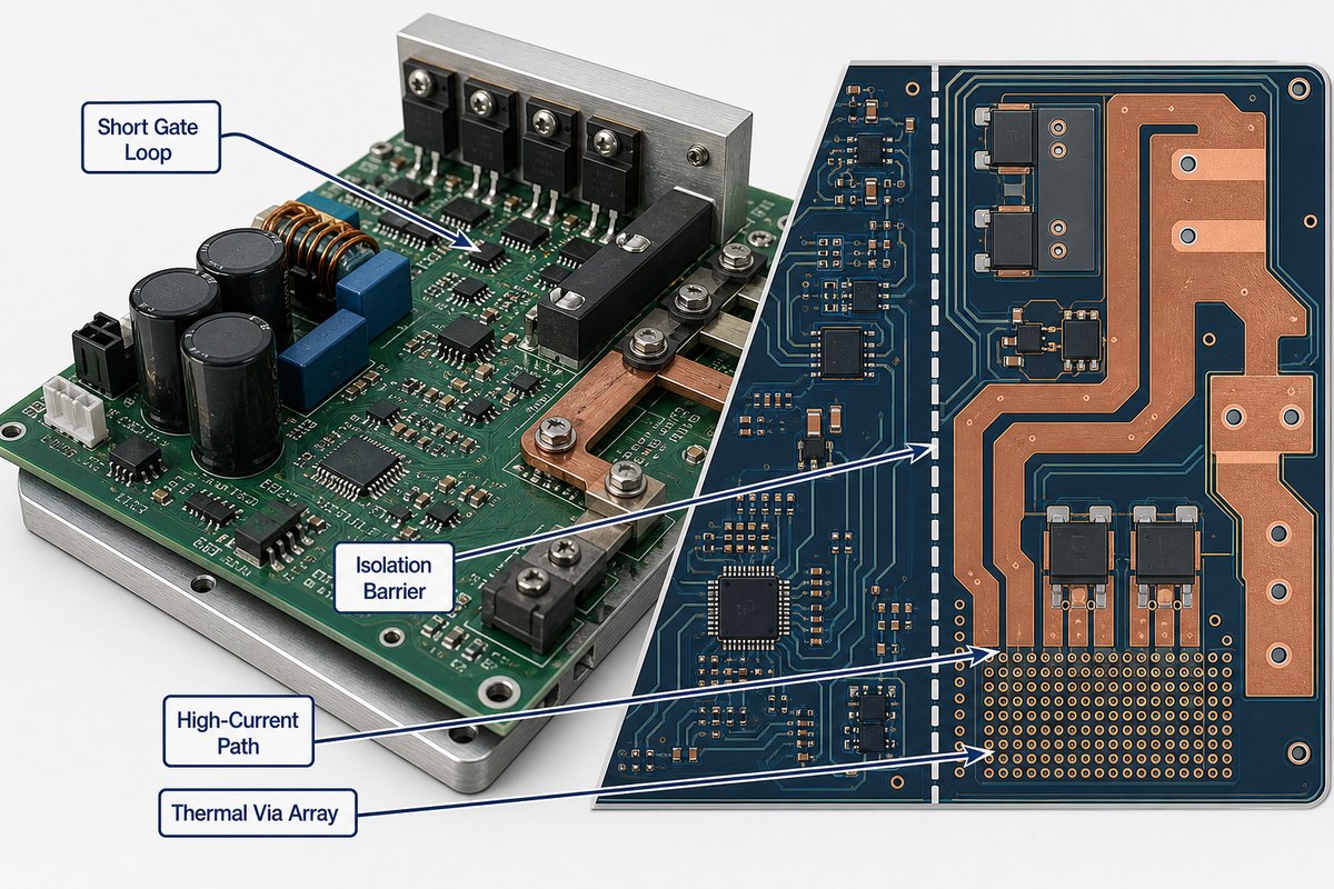
Moving from silicon IGBTs to faster SiC or GaN devices can expose layout weaknesses that were previously hidden. Faster edges can reduce switching loss, but the gate loop, common-source inductance, isolation capacitance, and measurement bandwidth need to be re-evaluated. A component substitution is not automatically a drop-in PCB change.
How Should High-Voltage Isolation Be Planned?
Working voltage alone is not enough to choose creepage, clearance, slots, or dielectric construction. The applicable end-product standard, insulation type, transient or impulse voltage, pollution degree, altitude, coating process, and material group all affect the required solution.
Map the isolation boundary across the complete assembly:
- PCB copper, pads, vias, mounting holes, slots, and board edges
- Transformers, optocouplers, digital isolators, relays, current sensors, and connectors
- Heat sinks, screws, brackets, shielding, chassis, and cable routing
- Contamination, condensation, coating coverage, and manufacturing tolerances
A routed slot can extend the surface path, but it does not automatically satisfy the air-clearance requirement. Solder mask is also not a universal substitute for qualified solid insulation. Our high-voltage PCB design guide explains why the final spacing must be tied to the actual insulation case instead of a generic voltage table.
How Do Copper and Thermal Design Affect Reliability?
Copper weight does not determine current capacity by itself. Conductor width and length, layer position, adjacent dielectric, via transitions, terminal contact, duty cycle, ambient temperature, enclosure airflow, heat-sink interface, and allowable temperature rise all influence the result.
Start with a loss map for semiconductor conduction and switching losses, magnetics, shunts, connectors, capacitors, relays, and copper paths. Then check the complete heat route from each source to copper planes, thermal vias, baseplate, heat sink, airflow, or enclosure. A large copper pour that ends in a thermally isolated region may spread heat locally without removing it from the assembly.
Heavy copper can reduce resistance and help spread heat, but it changes etching, lamination, drilling, plating, solder mask, copper balance, and reflow behavior. Our article on 4-layer heavy copper PCB design covers these manufacturing interactions in more detail.
For validation, measure the assembled unit under representative current, switching mode, battery charge/discharge direction, enclosure temperature, airflow, and duty cycle. Thermal images are useful for locating hot spots, but thermocouples or other calibrated measurements may be needed where emissivity or access makes an image misleading.
Which Materials and Stackups Suit Hybrid Inverter PCB Boards?
Most solar inverter pcbs and hybrid inverter control boards can begin with an FR-4-family construction, but the exact material system must be chosen from operating temperature, thermal cycling, insulation, CTI, copper weight, dimensional stability, CAF risk, and assembly profile. “High-Tg” alone does not describe all of those properties.
| Design Need | Construction Direction | What Must Be Confirmed |
|---|---|---|
| Mixed control and moderate-power functions | Multilayer FR-4 with deliberate reference planes and domain separation | Stackup, dielectric system, copper distribution, isolation, and impedance where needed |
| High-current power paths | Heavier copper, local bus structures, or separate power board | Etched geometry, plating, terminal transitions, thermal rise, and manufacturability |
| High heat flux near power packages | Thermal-via arrays, bonded heat spreader, metal-core sub-board, or ceramic option | Electrical isolation, attachment method, solder reliability, and real cooling path |
| Fast control or communications | Controlled multilayer return paths and impedance where the interface requires it | Trace geometry, reference transitions, loss budget, and fabrication tolerance |
A stackup should be reviewed with the fabricator before routing is frozen. Heavy outer copper can limit fine spacing; thick inner copper affects resin fill and lamination; mixed copper densities can worsen warpage; and isolation slots or large cutouts can weaken panel support. The optimum power board and control board may therefore use different constructions.
What Assembly Challenges Need Early DFM Review?
Hybrid inverter assemblies combine high-thermal-mass parts with dense control electronics. That creates competing stencil, placement, soldering, and inspection requirements. DFM should begin while component packages and mechanical interfaces can still change.
- Large terminals and bus connections: confirm hole tolerance, copper connection, mechanical load path, fastening access, and soldering method.
- Power packages: review exposed-pad geometry, void-sensitive joints, thermal vias, solder volume, heat-sink flatness, and mounting sequence.
- Mixed thermal mass: evaluate whether one reflow profile can heat large power joints without overstressing nearby small components.
- Tall and heavy parts: confirm placement clearance, polarity marking, adhesive or mechanical support, and vibration requirements.
- Isolation areas: keep flux residue, markings, test pads, copper thieving, tooling features, and coating keep-outs from compromising the designed barrier.
- Service connectors: check mating cycles, insertion forces, harness strain, and access after enclosure assembly.
Provide 3D mechanical data for heat sinks, busbars, capacitors, inductors, terminals, enclosure walls, and fasteners. A PCB can be electrically correct yet impossible to assemble without bending parts or loading solder joints.
How Should a Hybrid Inverter PCBA Be Tested?
Testing should be derived from the failure risks of each board. No single method proves conductor quality, solder integrity, measurement accuracy, isolation, communication, and system behavior at once.
- Bare-board verification: use netlist-based electrical testing or flying probe as appropriate, plus impedance, copper-thickness, and microsection checks where specified.
- Assembly process inspection: use visual inspection and AOI for presence, polarity, alignment, and visible joints.
- Hidden-joint inspection: apply X-ray where packages or power joints prevent adequate optical access.
- Low-energy bring-up: confirm rails, isolation interfaces, current-sense offsets, communications, programming, and protection logic before applying full bus energy.
- Functional verification: run the customer-defined fixture and limits for control states, I/O, relay sequencing, sensing, fault response, and communications.
- System validation: validate efficiency, temperature, EMI, grid behavior, battery transitions, surge/fault behavior, and product-standard requirements on a representative inverter assembly.
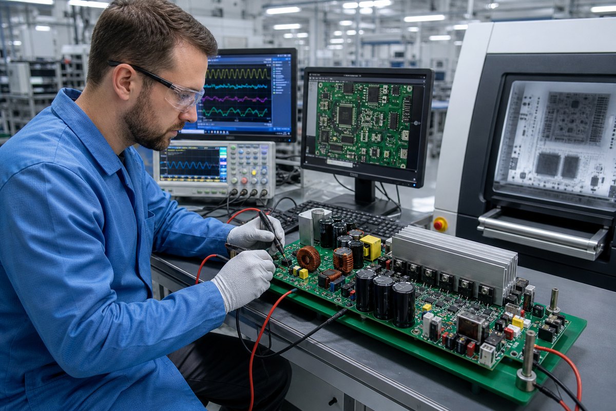
EBest Circuit can support AOI, X-ray inspection, functional testing, electrical/flying-probe testing, impedance testing, microsection inspection, and copper-thickness testing when they are defined for the project. Customer-owned firmware, fixtures, loads, pass/fail limits, and safety procedures should be identified before quotation so the production test scope is unambiguous.
What Common Failure Modes Should Be Designed Out?
Many inverter failures are system interactions that appear on the PCB. A useful design review traces the initiating condition, the electrical stress path, the thermal or mechanical consequence, and the test that can detect the weakness.
- Gate ringing or false turn-on: commonly linked to loop inductance, common-source coupling, poor gate return, excessive edge rate, or isolation parasitics.
- Current-sense instability: caused by switch-node coupling, weak reference routing, bandwidth mismatch, or shared high-current returns.
- Hot terminals and neck-downs: created when a wide copper region funnels through a pad, via field, connector, fuse, or layer transition.
- Isolation breakdown or tracking: associated with inadequate spacing, contamination, moisture, unreviewed slots, conductive hardware, or an incorrect insulation assumption.
- Cracked power joints: driven by thermal cycling, package-to-board CTE mismatch, heavy components, heat-sink stress, or mounting tolerance.
- Mode-transition resets: produced when auxiliary rails, ground references, communication links, or protection timing do not tolerate a sudden energy-flow change.
Do not treat a symptom such as “inverter PCB burned” as a root cause. Preserve fault logs, waveforms, failed parts, board location, operating mode, load, battery state, and environmental conditions for analysis.
What Files Are Needed for a Manufacturing Quote?
A complete RFQ lets the manufacturer evaluate board construction, assembly difficulty, inspection coverage, and material availability before price and lead time are committed.
- Gerber or ODB++ fabrication data, NC drill files, netlist, stackup, finished copper requirements, board thickness, surface finish, controlled-impedance table, and dimensional drawing
- BOM with manufacturer part numbers, approved alternates, do-not-substitute items, lifecycle concerns, and sourcing responsibility
- Centroid/pick-and-place file, assembly drawings, polarity and orientation notes, stencil requirements, and special soldering instructions
- Working and transient voltages, current and duty-cycle information, isolation classification, environmental conditions, applicable standards, and critical spacing dimensions
- Heat-sink, busbar, terminal, enclosure, hardware, and 3D mechanical data with torque or flatness requirements where applicable
- Programming files, functional-test procedure, fixture responsibility, test limits, required reports, sample approval plan, quantity, and delivery schedule
If the design is still evolving, mark assumptions and open items instead of hiding them. Early review of the solar inverter PCB manufacturing package can prevent a layout that works electrically but cannot be built or tested repeatably.
FAQ About Hybrid Inverter PCBs
What is the PCB in a hybrid inverter?
It is the printed circuit platform that supports power conversion, gate drive, sensing, protection, control, communications, or interface functions. A product may use one integrated PCB or several coordinated boards.
How is a hybrid inverter PCB different from a standard solar inverter PCB?
A hybrid design normally adds a battery energy path and the controls needed for bidirectional charging/discharging and multiple operating modes. That creates more interfaces, fault states, current directions, and transition conditions than a basic grid-tied PV inverter.
Can the power and control circuits share one PCB?
Yes, when the electrical, thermal, isolation, EMI, mechanical, and service requirements can all be met. Separating boards may be better at higher power or when different construction and cooling methods are needed.
Does every hybrid inverter need a heavy copper PCB?
No. Copper construction depends on current path, temperature rise, geometry, duty cycle, cooling, and assembly constraints. Busbars, separate power modules, or other structures may be preferable for some high-current paths.
Can SiC or GaN devices use the same layout as an IGBT design?
Not automatically. Faster switching can make gate-loop inductance, common-source inductance, isolation capacitance, switch-node coupling, measurement bandwidth, and EMI more critical. The PCB and gate-drive network should be reviewed with the selected device and operating conditions.
What determines the cost of Hybrid Inverter PCBs?
Major cost drivers include board size, layer count, copper construction, material system, via and slot requirements, controlled impedance, component availability, power-package assembly, inspection, fixtures, functional testing, order quantity, and required documentation. A complete package produces a more reliable quote than a schematic or photo alone.
How Can EBest Circuit Support Your Hybrid Inverter PCB Project?
At EBest Circuit, we support PCB design review, prototyping, fabrication, component sourcing, PCB assembly, and production transition for power and control electronics. Our relevant PCB options include multilayer, heavy copper, high-Tg, high-speed, impedance-control, metal-core, and ceramic constructions. Our documented quality and compliance credentials include ISO 9001:2015, IATF 16949, RoHS, REACH, and UL E502832; the applicable requirements and certification scope should still be confirmed for each program.
If you are preparing Hybrid Inverter PCBs for a new platform, we can review the board construction and assembly-sensitive details before the design enters production.
Send your Gerber or ODB++ data, BOM, stackup, quantity, operating voltage and current, isolation requirements, mechanical files, and test plan to sales@bestpcbs.com. We will review the fabrication, assembly, thermal, isolation, and test-sensitive details before quotation.
You may also like



Tags: hybrid inverter pcb, hybrid inverter pcb board, hybrid inverter pcb diagram, Hybrid Inverter PCBs, solar inverter pcbs