On September 3, 2026, OpenAI released GPT-6 Astra, its latest frontier AI model. OpenAI describes Astra as its most capable broadly deployed model to date, with major improvements in computer use, coding, research, and complex multistep work.
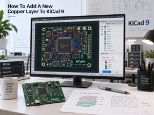
For PCB engineers, one demonstration stood out: Astra was shown working directly inside KiCad, placing components and routing a PCB from schematic data. The result is interesting not because AI suddenly replaces PCB engineers, but because PCB design is becoming another professional workflow that AI can actively operate rather than simply discuss.
That creates a useful question for electronics manufacturers:
If AI can generate a PCB layout, can that board actually be manufactured—and can it meet the signal, power, and reliability requirements of modern AI hardware?
Why Does GPT-6 Astra Matter to the PCB Industry?
GPT-6 Astra affects the PCB industry from two directions. First, AI is moving deeper into the engineering workflow itself, meaning tasks that once required direct manual operation inside EDA software may increasingly receive AI assistance, including:
- Component placement
- PCB routing
- Design-rule checking
- Revision comparison
- Documentation
- Library and data handling
- Layout optimization
The KiCad demonstration gives a practical example of this shift. AI no longer needs to stop at explaining how a PCB should be designed if it can interact with the same design tools engineers already use.
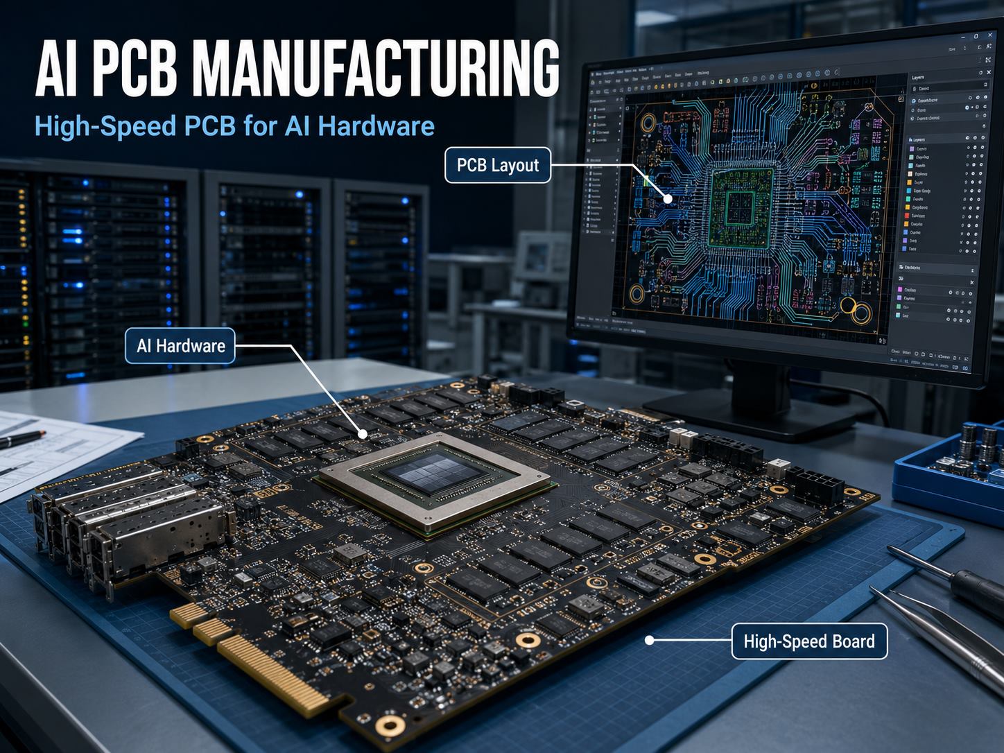
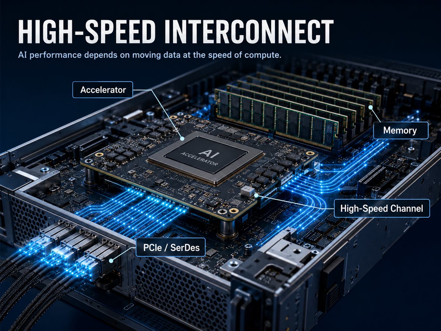
The second impact comes from the hardware required to run increasingly capable AI systems. AI servers depend on processors, GPUs, accelerators, high-bandwidth memory, network controllers, optical modules, storage devices, and power systems, all connected through hardware such as:
- Accelerator boards
- Server motherboards
- Network interface cards
- Switch boards
- Backplanes
- Storage boards
- Optical interface boards
As these systems move more data between devices, the PCB becomes part of the high-speed transmission channel rather than simply a platform for mounting components.
Can AI Design a Manufacturable PCB?
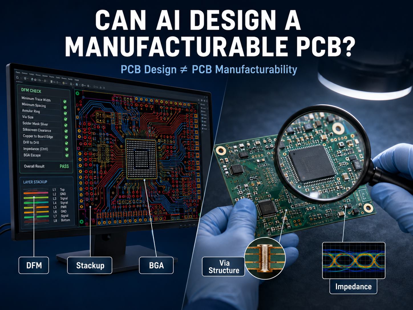
AI can help create a PCB layout, but manufacturability still depends on physical fabrication limits. A design may satisfy the rules defined in CAD and still create problems when it reaches the factory.
For example:
- A narrow trace may be valid in the layout but unsuitable for the specified copper thickness.
- A BGA escape may require microvias that were not included in the original stackup.
- A proposed prepreg thickness may not be practical for normal production.
- An impedance geometry may need adjustment once the actual laminate and copper thickness are confirmed.
- A long through-hole via may leave an undesirable stub on a high-speed channel.
- A complex stacked-microvia structure may add cost or reliability risk without being necessary.
This is where DFM goes beyond DRC. Design-rule checking determines whether a PCB follows a defined set of layout constraints, while manufacturing review determines whether those constraints can be reproduced consistently through drilling, plating, etching, lamination, surface finishing, assembly, and testing.
At EBest Circuit, our engineering review considers the released design together with its intended manufacturing process, including stackup, material, trace/space, copper thickness, via construction, controlled impedance, surface finish, and assembly requirements. AI may shorten the path to a completed layout, but the digital geometry still has to be converted into a stable production process.
Why Does the AGI Era Need High-Speed PCBs?
The connection comes down to data movement. AI accelerators constantly exchange data with memory, CPUs, neighboring accelerators, storage, and network interfaces, so increasing computing power without sufficient interconnect bandwidth leaves expensive processors waiting for data.
High-speed standards already show the direction of travel. PCIe 7.0 supports 128 GT/s raw data rate and up to 512 GB/s bidirectional bandwidth through an x16 link, using PAM4 signaling. PCI-SIG lists AI/ML, high-performance computing, hyperscale data centers, and other data-intensive applications among the markets driving this bandwidth increase.
At these speeds, the PCB channel has to control more than basic connectivity. Engineers must account for:
- Insertion loss
- Impedance discontinuities
- Crosstalk
- Differential skew
- Via transitions
- Return-path continuity
- Copper roughness
- Dielectric loss
A fabrication variation that has little practical effect on a low-speed control board may consume meaningful signal margin on an AI accelerator or server motherboard, which is why high-speed hardware demands tighter control over materials, geometry, stackup, and vias.
What Makes an AI High-Speed PCB Different From a Standard PCB?
There is no single specification for an “AI PCB.” The difference comes from what the board is required to carry. An accelerator board with high-speed serial interfaces has very different manufacturing requirements from a low-speed controller used elsewhere in the same server.
| Design Area | Conventional PCB | AI / High-Speed PCB |
| Signal environment | Often lower-speed | Multi-gigabit interfaces common |
| Material | Standard FR-4 often sufficient | Low-loss laminate may be needed |
| Impedance | Selected nets may be controlled | Often critical across many channels |
| Stackup | Standard construction possible | More tightly tied to SI and PI |
| Routing density | Low to moderate | Dense BGA escape common |
| Via structure | Through vias widely used | HDI or back drilling may be required |
| Power demand | Moderate | Higher current density possible |
| Verification | Electrical test | Impedance and tighter process control may be added |
Layer count alone does not define a high-speed PCB. A 20-layer board carrying slow control signals may have modest signal-integrity requirements, while a smaller board carrying a demanding SerDes interface can require much tighter material, geometry, and impedance control.
Which PCB Materials Are Suitable for AI and High-Speed Computing?
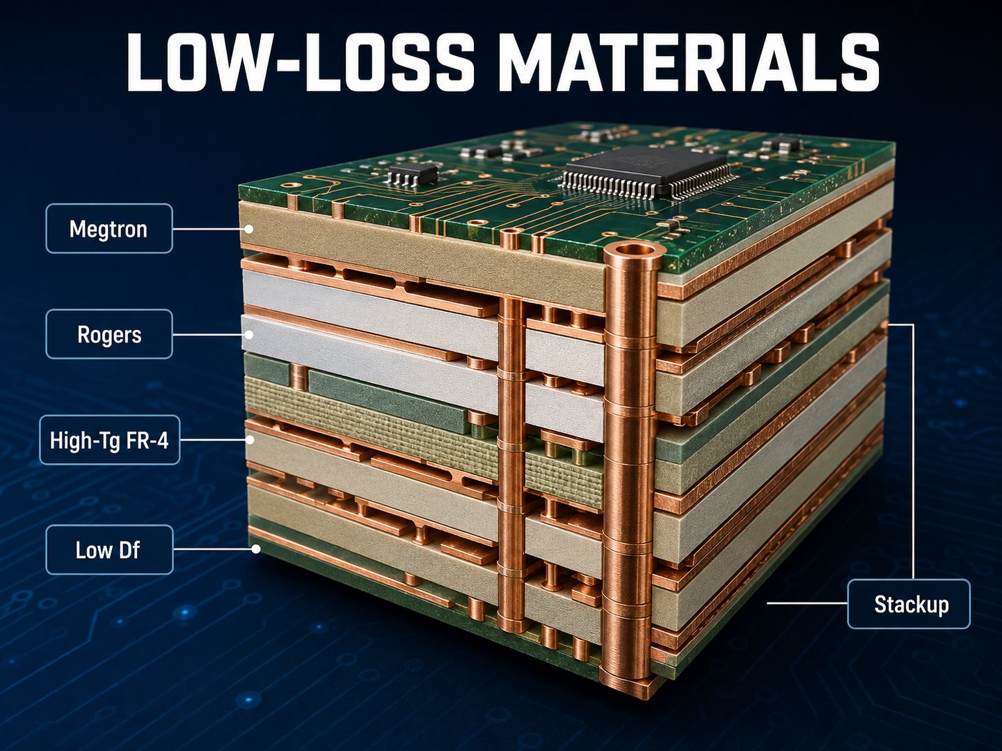
Material selection should begin with the channel loss requirement rather than the most expensive laminate available. Depending on the interface speed and routing architecture, suitable materials may include:
- High-Tg FR-4
- Low-loss FR-4
- Panasonic Megtron families
- Rogers laminates
- Other low-Dk / low-Df systems
The lowest Df value is not automatically the right choice. Engineers should also consider:
- Data rate
- Channel length
- Dielectric thickness
- Impedance geometry
- Copper profile
- Glass weave
- Thermal reliability
- Lamination structure
- Material availability
- Cost
For shorter channels or less demanding interfaces, a good low-loss FR-4 system may already provide sufficient performance. Longer channels with tighter insertion-loss budgets may justify a more specialized laminate.
EBest Circuit supports high-Tg FR-4, Rogers, Megtron, and other project-specific low-loss materials. When the design is still being developed, confirming the laminate family and production stackup before routing is finalized can prevent later changes to trace width, spacing, or impedance geometry.
Why Is Controlled Impedance Critical for AI Server PCBs?
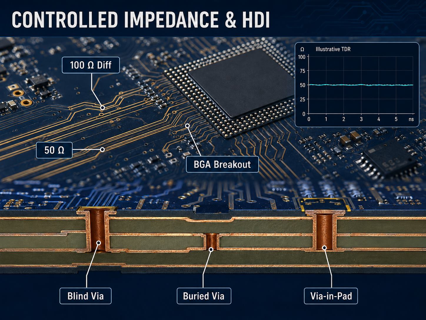
High-speed traces behave as transmission lines, so their impedance has to remain within the intended channel design. Typical targets may include 50 Ω single-ended, 90 Ω differential, or 100 Ω differential, although the correct value always comes from the interface specification.
Actual PCB impedance depends on several physical variables:
- Trace width
- Finished copper thickness
- Differential-pair spacing
- Dielectric thickness
- Material Dk
- Distance to the reference plane
- Etching compensation
Controlled impedance is therefore both a design requirement and a manufacturing requirement. A nominal 100 Ω pair in CAD does not guarantee a 100 Ω result after fabrication; the final trace geometry needs to correspond to the actual production stackup.
For high-speed projects, EBest Circuit can review the stackup and impedance geometry before production and perform TDR impedance verification when required. The fabrication package should clearly identify the impedance target, tolerance, layer, material, and copper requirement so these parameters can be checked before the board enters production.
Why Are HDI and Advanced Vias Important for AI Accelerator PCBs?
Large processors, FPGAs, accelerators, and memory packages can place thousands of connections inside a compact BGA footprint. Conventional plated through-holes occupy routing space through the full board thickness, so denser packages may require more efficient breakout structures.
Depending on the architecture, HDI options can include:
- Laser microvias
- Blind and buried vias
- Via-in-pad
- Filled and plated vias
- Staggered microvias
- Stacked microvias
- Sequential lamination
Shorter vertical transitions can reduce some of the electrical discontinuity associated with long through-hole vias. Where through-hole routing remains appropriate, back drilling may be used on selected high-speed channels to remove unused via stubs.
More complexity is not automatically better. Stacked microvias require additional processing and introduce their own reliability considerations, so if a staggered structure or conventional via construction satisfies the routing and signal requirements, adding another lamination cycle may offer little practical benefit.
EBest Circuit supports HDI, laser microvias, blind and buried vias, via-in-pad, and filled-via structures according to the actual BGA fanout and routing requirements.
How Do Power and Thermal Demands Affect AI PCB Manufacturing?
High-speed signaling is only one challenge in AI hardware; power density is the other. Accelerator boards may need substantial current delivered through a compact area, which affects both stackup planning and copper distribution.
Common PCB considerations include:
- Dedicated power and ground planes
- Wider high-current copper paths
- Dense power/ground via arrays
- Low-inductance decoupling paths
- Thermal vias
- Local copper balancing
- PDN planning
- Warpage control
Power integrity and signal integrity also interact. A poor return path can affect a high-speed channel even when trace width and nominal impedance are correct, while supply noise can reduce the voltage and timing margin available to fast interfaces.
Manufacturing also has to account for copper distribution. Heavy or uneven copper can influence resin flow, lamination behavior, finished thickness, and board flatness. On high-layer-count server and accelerator boards, the stackup therefore has to balance signal routing, reference planes, power delivery, thermal behavior, and manufacturability rather than optimizing each factor independently.
What Should Engineers Check Before Sending an AI PCB to Production?
For an AI accelerator or high-speed computing board, a complete manufacturing package reduces avoidable engineering loops before fabrication.
Before release, confirm:
- Final Gerber or ODB++ revision
- Fabrication drawing
- Layer stackup
- Exact material grade or approved substitutions
- Finished copper weight
- Finished board thickness
- Controlled-impedance table and tolerance
- BGA pitch
- Through/blind/buried/microvia structure
- Via-in-pad and filling requirements
- Back-drill requirements
- Surface finish
- Electrical and impedance testing
- BOM and pick-and-place files for PCBA
- Assembly drawing
The best time to resolve stackup, material, and impedance conflicts is before routing is fully locked. For technically demanding boards, an early fabricator review can prevent later changes to trace geometry, BGA breakout, or via structure after the production stackup has already been established.
AI PCB Manufacturing Case Studies from EBest Circuit
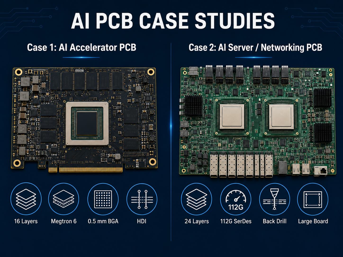
The following two representative cases show how the manufacturing priorities change between a dense AI accelerator PCB and a larger AI server or networking board.
Case 1: High-Speed AI Accelerator PCB
Project: 16-layer low-loss PCB for an AI accelerator platform, with controlled differential impedance and dense BGA routing.
Specifications:
- Layer count: 16 layers
- Low-loss material / material brand: Panasonic Megtron 6
- Finished thickness: 2.0 mm
- Copper weight: 1 oz outer / 0.5–1 oz inner
- Controlled impedance: 50 Ω single-ended / 100 Ω differential
- Fine-pitch BGA: 0.5 mm pitch
- HDI / blind via / microvia / via-in-pad: Microvia + blind via + via-in-pad
- TDR testing: Yes
- Surface finish: ENIG
- Prototype quantity: 20 pcs
- PCBA / X-ray if applicable: SMT + BGA X-ray
This project mainly challenged dense BGA breakout, impedance consistency, and high-speed signal loss. The HDI structure provided more routing space around the fine-pitch package, while the low-loss material and controlled stackup supported stable high-speed transmission. It also shows why stackup and via structure should be confirmed with the fabricator before a dense accelerator layout is completely frozen.
Case 2: AI Server / High-Speed Networking PCB
Project: High-layer-count PCB for AI server and high-speed networking hardware, with high-speed SerDes routing and demanding power-distribution requirements.
Specifications:
- High layer count: 24 layers
- PCIe / high-speed SerDes related routing: PCIe / 112G SerDes
- Multiple controlled impedance values: 50 Ω / 85 Ω / 100 Ω
- Back drilling: Selected high-speed vias
- Large board size: 420 × 330 mm
- Tight finished thickness: 3.2 mm
- Low-loss stackup: Megtron 6
- High-current power/ground planes: Up to 2 oz
- Warpage control: ≤0.5%
- SMT + BGA X-ray: Yes
- Functional or electrical testing: Electrical test + TDR
This project placed more pressure on long high-speed channels, via-stub control, stackup stability, and board flatness. Back drilling and controlled impedance addressed the signal path, while copper balance and multilayer lamination control helped maintain dimensional stability on the larger board. Compared with the accelerator board, manufacturing control has to cover both electrical performance and the mechanical behavior of a large, thick multilayer PCB.
How Can EBest Circuit Support High-Speed PCB Manufacturing for AI Hardware?
EBest Circuit supports high-speed PCB and PCBA projects from manufacturing review through prototype and volume production. Instead of applying the same process to every AI-related board, we match the manufacturing route to the actual electrical, mechanical, and reliability requirements.
| AI Hardware Requirement | EBest Circuit Support |
| High-speed channels | Controlled-impedance fabrication |
| Low channel loss | High-Tg FR-4, Megtron, Rogers and other low-loss materials |
| Dense BGA breakout | HDI, microvia and via-in-pad |
| Complex layer architecture | Multilayer PCB manufacturing |
| Impedance verification | TDR testing when specified |
| Production risk review | DFM and stackup review |
| Dense SMT assembly | SMT, AOI and X-ray |
| Prototype to production | PCB + PCBA support |
With more than 20 years of PCB and PCBA manufacturing experience and production support in China and Vietnam, we work with high-speed computing, networking, accelerator, and other data-intensive electronics.
The engineering objective is not to maximize layer count or specify the most expensive laminate. The better approach is to meet the required bandwidth, routing density, reliability, and production yield without adding process complexity that the design does not need.
What Does GPT-6 Astra Mean for the Future of PCB Engineering?
GPT-6 Astra’s KiCad demonstration gives a useful indication of how PCB design workflows may change. AI is likely to become more involved in tasks such as:
- Initial placement and routing
- Constraint checking
- Documentation
- Design comparison
- Data preparation
- Repetitive layout optimization
The manufacturing side remains physical. Copper still has to be etched, holes drilled and plated, and multilayer structures laminated within real process tolerances. Materials have actual Dk values, prepregs have available thicknesses, microvias have reliability limits, and finished boards still have to survive assembly and operate inside real electrical and thermal margins.
AI may become much faster at creating electronic designs, but turning those designs into reliable hardware will still depend on disciplined PCB engineering and manufacturing.
Frequently Asked Questions
1. Can GPT-6 Astra design a PCB?
Yes. OpenAI demonstrated GPT-6 Astra operating KiCad from an electronic schematic, performing component placement and PCB routing. This shows that a general-purpose AI system can now directly interact with professional PCB design software rather than only provide written design guidance.
2. Can AI design a manufacturable PCB?
AI can generate or assist with layouts that satisfy defined design rules, but manufacturability still depends on real fabrication constraints. Stackup, material availability, copper thickness, trace/space, impedance, via structure, plating, assembly, and reliability should still be reviewed before release.
3. Will AI replace PCB layout engineers?
AI is likely to automate some PCB layout and verification tasks, particularly repetitive work. Complex designs still require engineering judgment involving SI/PI, power delivery, component packaging, mechanical constraints, reliability, DFM, and manufacturing feedback.
4. Why do AI servers need high-speed PCBs?
AI servers contain accelerators, processors, memory, storage, and networking devices that exchange large volumes of data. The PCB carries many of those signals, so insertion loss, impedance, via transitions, return paths, crosstalk, and fabrication tolerance can affect high-speed channel performance.
5. What PCB materials are used for AI accelerator boards?
The material depends on the interface speed, channel length, loss budget, thickness, stackup, and cost. Options can range from high-Tg FR-4 to low-loss FR-4, Megtron, Rogers, and other low-Dk/low-Df systems. Not every AI accelerator PCB requires Rogers or another premium laminate.
6. What files should I send for a high-speed AI PCB quote?
For an accurate engineering review, provide the Gerber or ODB++ files, fabrication drawing, stackup, material requirement, copper weight, finished thickness, impedance table, drill/via information, and testing requirements. For assembly, also include the BOM, pick-and-place data, and assembly drawing.
If you are developing an AI accelerator PCB, AI server motherboard, high-speed computing board, HDI PCB, or controlled-impedance project, send your Gerber files, stackup, impedance requirements, BOM, and assembly specifications to sales@bestpcbs.com. Our engineering team can review the project before production and help confirm the appropriate material, stackup, via structure, impedance-control, and manufacturing approach.