PCB manufacturing PCB manufacturing
Home > Blog

IPC-TM-650 PCB Test Methods Manual

April 29th, 2026

What Is the IPC-TM-650 Test Methods Manual?

IPC-TM-650 test methods manual is a collection of standardized test procedures used to evaluate printed circuit boards, PCB materials, assemblies, and connectors. It helps PCB manufacturers, quality engineers, and buyers use the same technical language when discussing cleanliness, plating quality, solder mask reliability, electrical insulation, environmental stress, and mechanical stability.

In simple words, IPC-TM-650 tells people how to test a PCB-related item. It does not always tell people whether the result is acceptable for every project. The pass/fail requirement often comes from customer specifications, IPC product standards, procurement documents, or industry-specific quality requirements.

For PCB production, IPC-TM-650 is often used for:

  • PCB cleanliness verification
  • Bow and twist measurement
  • Solder mask reliability testing
  • Microsection analysis
  • Surface insulation resistance testing
  • CAF resistance evaluation
  • Thermal stress and thermal shock testing
  • Material electrical and mechanical property checks
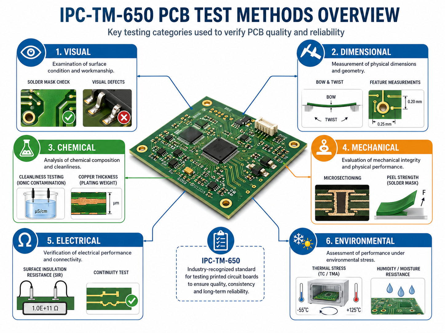
IPC-TM-650 PCB Test Methods Manual

Why Is IPC-TM-650 Important for PCB Manufacturing Quality?

IPC-TM-650 is important because it gives PCB manufacturers and customers a consistent way to verify quality. Without a shared test method, one supplier may test cleanliness in one way, another may use a different extraction method, and a customer may struggle to compare results fairly.

It supports quality control in several practical areas:

  • Process control: checking whether manufacturing steps remain stable from batch to batch
  • Failure analysis: identifying the possible cause of leakage, corrosion, delamination, or solder mask failure
  • Supplier qualification: checking whether a PCB supplier can meet reliability expectations
  • Design verification: confirming that stack-up, materials, hole structure, and solder mask choices fit the application
  • High-reliability production: supporting medical, automotive, aerospace, telecom, power electronics, and industrial control projects

A PCB factory that understands these testing methods can usually communicate better during DFM review, material selection, production validation, and quality troubleshooting.

What Test Categories Are Included in IPC-TM-650?

IPC-TM-650 covers multiple test categories, including visual, dimensional, chemical, mechanical, electrical, environmental, and connector-related test methods. These categories help users quickly find the right method for a specific quality concern.

IPC-TM-650 CategoryMain Test FocusPCB Manufacturing RelevanceTypical Examples
Visual Test MethodsInternal and external observationHelps inspect plating, holes, laminate structure, and visible defectsMicrosectioning, plated-through hole evaluation
Dimensional Test MethodsSize, thickness, flatness, hole positionHelps control board geometry and assembly fitBow and twist, thickness, hole location
Chemical Test MethodsResidues, contamination, chemical propertiesHelps evaluate cleanliness and process residuesROSE, ion chromatography, organic contamination
Mechanical Test MethodsStrength, adhesion, peel, material behaviorHelps validate copper adhesion, solder mask durability, and flexible material strengthPeel strength, adhesion, abrasion
Electrical Test MethodsResistance, dielectric strength, signal performanceHelps evaluate insulation, high-voltage behavior, and RF propertiesSIR, dielectric strength, impedance-related tests
Environmental Test MethodsHumidity, heat, thermal cycling, agingHelps predict long-term reliability under service conditionsThermal shock, CAF, moisture resistance
Connector Test MethodsConnector durability and electrical behaviorHelps validate connector-level reliabilityContact resistance, vibration, humidity

What Is IPC-TM-650 Cleanliness Testing?

IPC-TM-650 cleanliness testing evaluates contamination, ionic residues, flux residues, process chemicals, and other materials that may remain on a PCB or PCBA surface. In PCB manufacturing, cleanliness is closely linked to insulation resistance, corrosion resistance, electrochemical migration, and field reliability.

Cleanliness is especially important when a board works in:

  • High humidity
  • High voltage
  • High impedance circuits
  • Medical monitoring equipment
  • Automotive control modules
  • Industrial sensors
  • Telecom infrastructure
  • Aerospace or defense electronics

A small amount of ionic residue may not create an immediate failure during final electrical testing. However, when moisture, voltage bias, and time are added, residues can support leakage paths, dendritic growth, corrosion, and unstable electrical behavior.
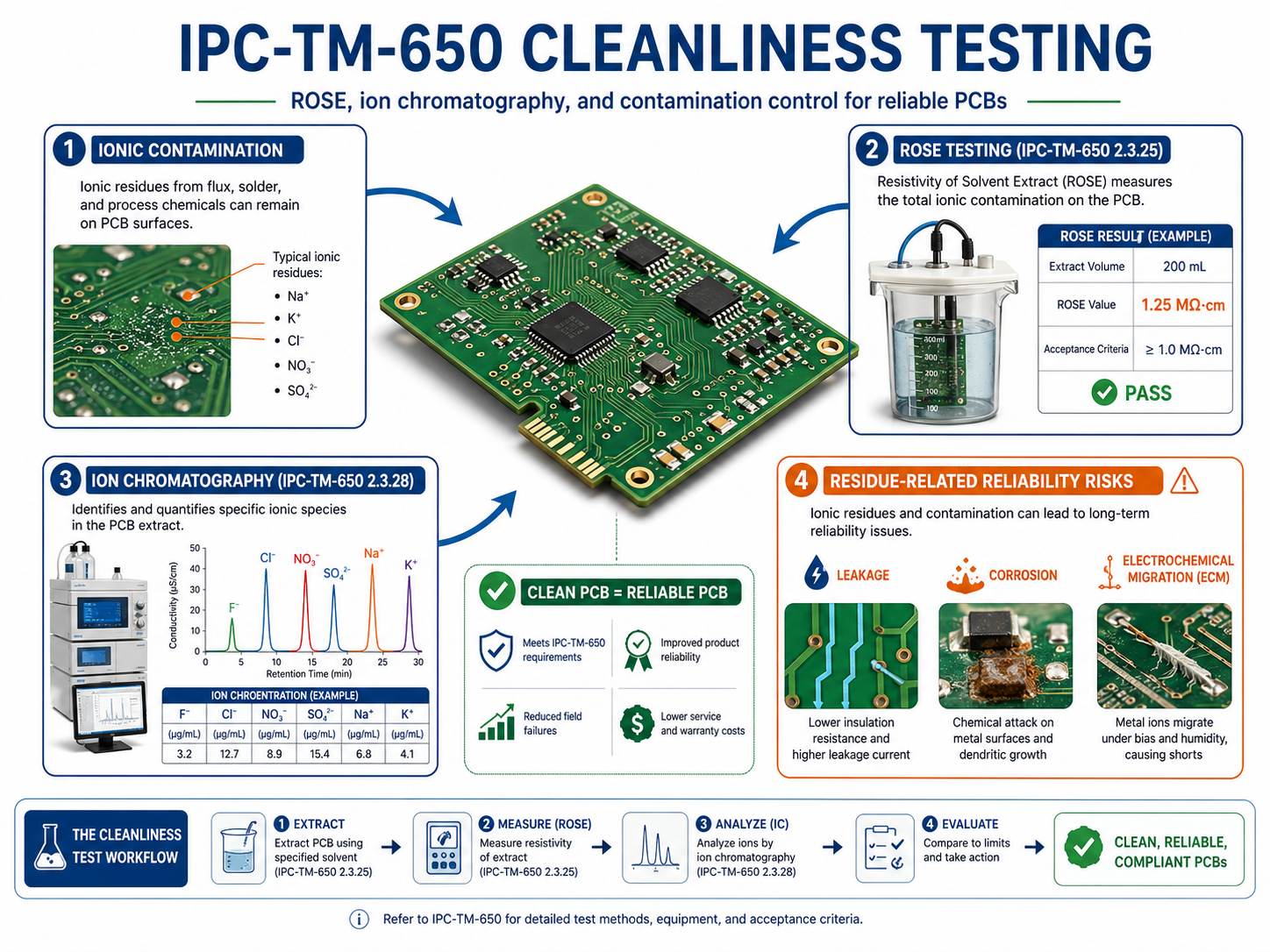
What Is IPC-TM-650 Cleanliness Testing?

IPC-TM-650 includes methods related to cleanliness and insulation performance, including surface insulation resistance and bare board cleanliness by SIR in the approved environmental test method list.

Cleanliness-Related TestWhat It ChecksBest Used ForPractical Value
ROSE TestOverall ionizable surface contaminationRoutine process controlFast cleanliness screening
Ion ChromatographySpecific ionic species and concentrationFailure analysis and high-reliability projectsFinds contamination source more precisely
SIR TestInsulation behavior under humidity and electrical biasCleanliness validation under stressShows reliability impact of residues
Visual InspectionVisible residue, staining, white marks, process contaminationInitial quality screeningSimple but not enough alone
Process AuditCleaning chemistry, rinse quality, drying, handlingManufacturing controlHelps prevent repeat issues

What Is IPC-TM-650 2.3.25 ROSE Testing for PCB Cleanliness?

IPC-TM-650 2.3.25 ROSE testing is commonly used to evaluate ionizable surface contaminants on PCB or PCBA surfaces. ROSE stands for Resistivity of Solvent Extract. It gives a fast cleanliness indicator, often reported as sodium chloride equivalent per unit area.

ROSE testing is useful because it is fast, repeatable, and suitable for production monitoring. If a PCB factory needs to compare different batches, check a cleaning process, or monitor contamination trends, ROSE can provide a practical baseline.

However, ROSE testing has a limitation. It measures total ionizable contamination, but it does not identify every individual ion. For example, a high ROSE reading may suggest contamination, but it may not tell whether the issue comes from chloride, bromide, weak organic acids, sodium, plating chemistry, flux residue, or handling contamination.

That is why ROSE is often used as a process control tool, while ion chromatography is used when a more detailed contamination profile is needed.

Good use cases for ROSE testing include:

  • Routine PCB cleanliness monitoring
  • PCBA cleaning process validation
  • Supplier quality comparison
  • Batch-to-batch contamination trend review
  • Quick screening before deeper analysis

For high-reliability products, ROSE alone may not be enough. It should be combined with ion chromatography, SIR, process traceability, and application-specific acceptance criteria.

What Is IPC-TM-650 2.3.28 Ion Chromatography Testing?

Ion chromatography is a more detailed cleanliness analysis method because it can identify and quantify specific ionic species. While ROSE gives an overall contamination value, ion chromatography helps show what type of contamination is present.

This matters in real PCB failure analysis. A board may show leakage current, corrosion, or dendritic growth after field use. A general contamination number may confirm that residue exists, but it may not explain the source. Ion chromatography can help identify whether the residue is related to process chemistry, flux activators, handling, water quality, or environmental exposure.

Typical ions that may be evaluated include:

  • Chloride
  • Bromide
  • Sulfate
  • Nitrate
  • Sodium
  • Potassium
  • Weak organic acids
  • Other process-related ionic species

Ion chromatography is especially valuable for medical electronics, automotive electronics, aerospace electronics, high-voltage PCB, and precision sensor circuits. In these products, contamination is not only a cosmetic concern. It can become a long-term electrical reliability risk.

What Is IPC-TM-650 2.6.3.7 Surface Insulation Resistance Testing?

IPC-TM-650 2.6.3.7 surface insulation resistance (SIR) testing evaluates how well a PCB surface maintains electrical insulation under humidity, temperature, and electrical bias.

SIR testing is important because many contamination problems do not appear during normal room-temperature inspection. A board may pass final electrical testing immediately after production. But after exposure to moisture and voltage bias, residues may become conductive enough to reduce insulation resistance.

The official IPC TM-650 method list includes TM 2.6.3.7 as “Surface Insulation Resistance.”
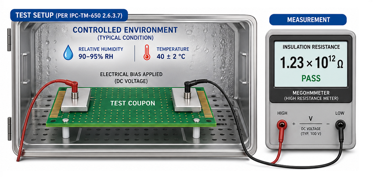
IPC-TM-650 2.6.3.7 Surface Insulation Resistance Testing

In practical PCB production, SIR testing can help evaluate:

  • Whether a cleaning process is reliable
  • Whether solder mask materials maintain insulation under humidity
  • Whether residues create leakage paths
  • Whether no-clean flux residues are acceptable for the application
  • Whether high-impedance circuits will remain stable over time
  • Whether bare boards or assemblies are suitable for harsh environments

SIR should be considered when a PCB uses dense spacing, fine-pitch components, high voltage, no-clean processes, or sensitive analog circuits. It is also useful when qualifying a new solder mask, flux, cleaning process, or assembly supplier.

What Is IPC-TM-650 Bow and Twist Testing?

IPC-TM-650 bow and twist testing is used to evaluate PCB flatness. Bow refers to a board bending in a smooth curved shape, while twist refers to diagonal warpage where the corners are not on the same plane.

Flatness IssueWhat It Looks LikeMain Assembly RiskCommon Design or Process Cause
BowBoard bends like a shallow arcUneven solder paste transfer, placement offsetThin board, large panel, unbalanced copper
TwistBoard corners lift diagonallyConnector misalignment, BGA open jointsAsymmetric stack-up, laminate stress
Local WarpageOne area lifts or deformsFine-pitch soldering defectLocal copper imbalance or heat concentration
Panel WarpageFull production panel bendsRouting, depaneling, and handling issuesPanel size, material stress, thermal exposure

Bow and twist control is especially important for:

  • Thin PCB
  • Large-size PCB
  • HDI board
  • BGA assembly
  • Fine-pitch QFN and LGA packages
  • Press-fit connector boards
  • Automotive control boards
  • LED panels
  • Rigid-flex boards
  • Boards with uneven copper distribution
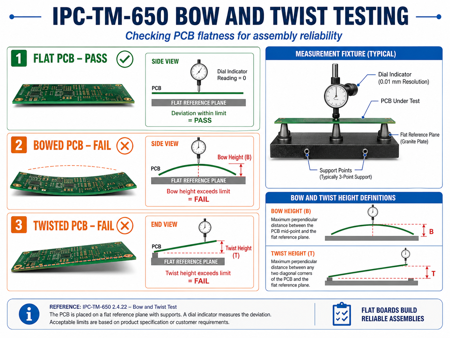
IPC-TM-650 Bow and Twist Testing

How Does Bow and Twist Affect PCB Assembly Reliability?

Excessive bow and twist can reduce assembly yield and long-term solder joint reliability. A PCB may still pass bare board electrical testing, but poor flatness can create serious problems during SMT assembly.

During solder paste printing, a warped board may not contact the stencil evenly. This can create insufficient solder paste in some areas and excess paste in others. During placement, small chip components may sit at different heights. During reflow, BGA or QFN packages may not maintain uniform contact with solder deposits.

The risks become more serious as component pitch becomes smaller. Common reliability problems caused by poor flatness include:

  • Open solder joints
  • Insufficient solder fillet
  • BGA non-wet open defects
  • Connector seating failure
  • Uneven mechanical stress after assembly
  • Housing fit problems
  • Local solder cracking during field vibration
  • Lower first-pass assembly yield

What Are IPC-TM-650 Testing Methods for Solder Mask?

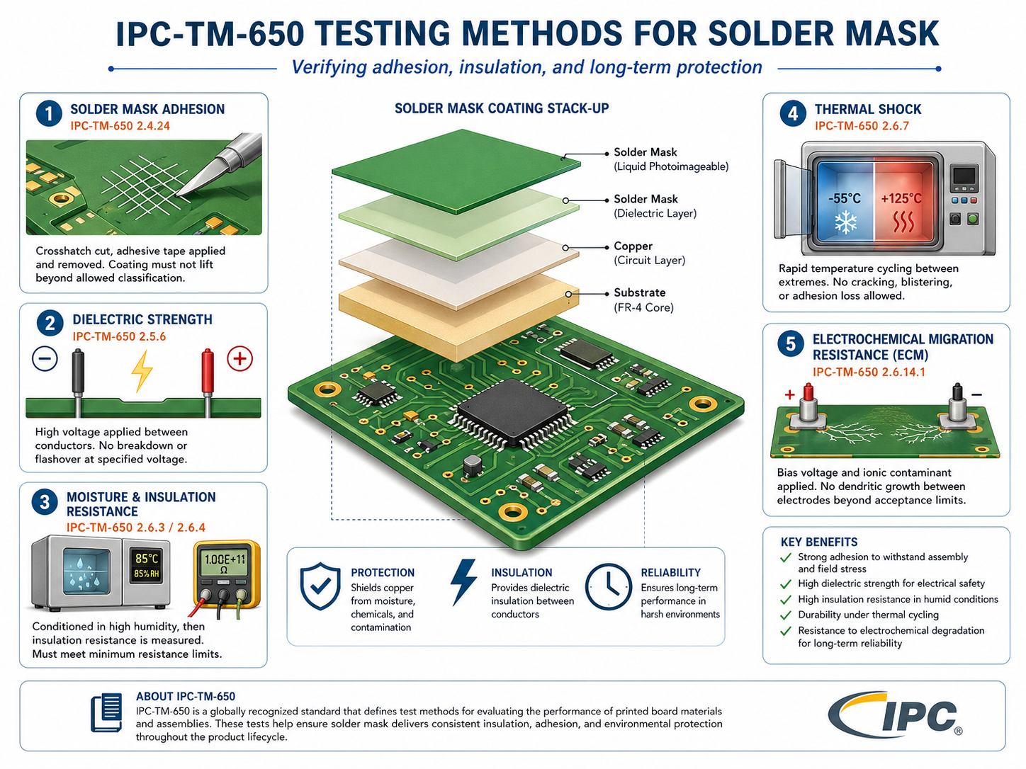
IPC-TM-650 testing methods for solder mask help evaluate whether the solder mask can protect copper, maintain insulation, resist humidity, withstand thermal stress, and support long-term PCB reliability.

Solder mask is more than the green, blue, black, white, or red coating seen on a finished PCB. It protects copper traces, defines solderable areas, reduces solder bridging, and supports electrical insulation between conductors.

Poor solder mask performance can cause:

  • Solder bridging
  • Copper exposure
  • Mask peeling
  • Blistering
  • Cracking after reflow
  • Chemical attack from cleaning agents
  • Leakage under humidity
  • Electrochemical migration risk

The IPC TM-650 method list includes solder-mask-related methods such as solder mask dielectric strength, solder mask moisture and insulation resistance, solder mask thermal shock, solder mask hydrolytic stability, and solder mask resistance to electrochemical migration.
What Are IPC-TM-650 Testing Methods for Solder Mask?

How Is IPC-TM-650 Different from IPC-A-600, IPC-6012, and IPC-A-610?

IPC-TM-650 explains how to test, while other IPC documents often define what is acceptable. This difference is important because many buyers ask for “IPC standard” without knowing which document applies to the problem.

DocumentMain PurposeSimple ExplanationCommon Use
IPC-TM-650Test methods manualExplains how to perform testsCleanliness, SIR, bow and twist, solder mask tests
IPC-A-600Acceptability of printed boardsShows acceptable and non-acceptable bare board conditionsVisual inspection of bare PCBs
IPC-6012Performance specification for rigid PCBsDefines rigid PCB performance requirementsRigid board procurement and quality control
IPC-A-610Acceptability of electronic assembliesDefines PCBA workmanship acceptanceSMT assembly and solder joint inspection
Customer SpecificationProject-specific acceptance requirementDefines what the customer expectsSpecial reliability, materials, and reporting needs

Which IPC-TM-650 Test Methods Should You Choose for Your PCB Project?

The right IPC-TM-650 test depends on the product application, failure risk, PCB structure, operating environment, and customer requirement. A simple consumer board does not always need the same test plan as a medical, automotive, aerospace, or power electronics PCB.

The goal is not to order every possible test. The goal is to choose the tests that reduce the most relevant risk.

PCB Project TypeRecommended IPC-TM-650 Related Tests
HDI PCBMicrosectioning, CAF, SIR, thermal stress
Automotive PCBBow and twist, CAF, thermal cycling, SIR
Medical PCBCleanliness, ion chromatography, SIR, traceability report
RF PCBDk/Df, signal loss, dimensional stability
Power PCBDielectric strength, thermal stress, CAF, solder mask insulation
Rigid-Flex PCBPeel strength, bend reliability, microsectioning
Fine-Pitch SMT PCBBow and twist, solder mask registration, cleanliness
Solder Mask Critical PCBSolder mask dielectric strength, moisture resistance, thermal shock

For early-stage prototypes, microsectioning and basic dimensional checks may be enough. For mass production, the test plan should be more structured.

How Should You Read an IPC-TM-650 Test Report?

A useful IPC-TM-650 test report should show more than a pass/fail result. It should tell the reader which method was used, how the sample was prepared, what condition was applied, what result was measured, and how that result connects to the project requirement.

A weak report says, “Passed.” While a strong report explains the evidence.

When reviewing an IPC-TM-650 test report, check the following items:

  • Test method number
  • Test method revision
  • Sample name and part number
  • Production lot number
  • Material type and stack-up
  • Surface finish
  • Sample quantity
  • Test condition
  • Test duration
  • Equipment used
  • Calibration status
  • Measurement result
  • Acceptance criteria source
  • Photos, charts, or microsection images
  • Technician or engineer review
  • Final conclusion
  • Traceability information

For high-value PCB projects, test reports should be stored as part of the quality record. They may become important during customer audits, field failure review, design changes, and supplier qualification.

How to Choose a PCB Manufacturer with IPC-TM-650 Testing Capability?

A capable PCB manufacturer should understand IPC-TM-650 as a practical quality tool, not just a document name. The supplier should know which test applies, when it should be used, what result format is expected, and how the result affects manufacturing decisions.

When selecting a PCB supplier, ask specific questions. Do not only ask, “Can you make IPC-quality boards?”

Ask:

  • Can you provide IPC-TM-650 cleanliness testing support?
  • Can you measure bow and twist for thin or large-size boards?
  • Can you support solder-mask-related reliability testing when needed?
  • Can you provide microsection images for plated holes and microvias?
  • Can you support SIR or CAF testing for high-reliability products?
  • Can you link test results to production lots and material batches?
  • Can your engineering team review stack-up, copper balance, and process risks before production?
  • Can you explain whether a test result meets our project-specific requirement?

A strong supplier will not recommend unnecessary testing just to increase cost. Instead, the supplier should help match the test plan to the project risk.

For example, a simple 2-layer prototype may need only basic electrical test and visual inspection. A 12-layer automotive control board may need microsectioning, thermal stress, CAF review, cleanliness control, and bow and twist monitoring. A medical sensing PCB may require cleanliness testing, SIR validation, and strict traceability.

Testing capability is part of reliability. Engineering judgment is the other part.

FAQs About IPC-TM-650 Test Methods

1. What is the IPC-TM-650 test methods manual?

IPC-TM-650 test methods manual is a collection of standardized testing procedures for printed circuit boards, materials, assemblies, and connectors. It covers visual, dimensional, chemical, mechanical, electrical, environmental, and connector-related testing. It helps PCB manufacturers and customers evaluate quality using consistent methods.

2. Is IPC-TM-650 the same as IPC-A-600?

No. IPC-TM-650 explains how to perform PCB-related tests. IPC-A-600 focuses on the acceptability of printed boards. In simple words, IPC-TM-650 is about testing procedures, while IPC-A-600 is about inspection and acceptance of bare PCB conditions.

3. When should I request IPC-TM-650 testing from a PCB supplier?

You should request IPC-TM-650 testing when your PCB has reliability-sensitive requirements, such as high voltage, fine spacing, high impedance, medical use, automotive use, harsh environment exposure, strict cleanliness needs, or complex multilayer construction. It is also useful during supplier qualification and failure analysis.

4. Does every PCB project need IPC-TM-650 testing?

Not every PCB project needs the full range of IPC-TM-650 testing. A simple prototype may only need basic inspection and electrical test. High-reliability boards, dense HDI boards, medical electronics, automotive electronics, power boards, and RF boards often need a more complete test plan.


You may also like

Mouse Bites PCB Guide: Dimensions, V-Cut Comparison, and Design Tips

April 29th, 2026

What Are Mouse Bites in PCB?

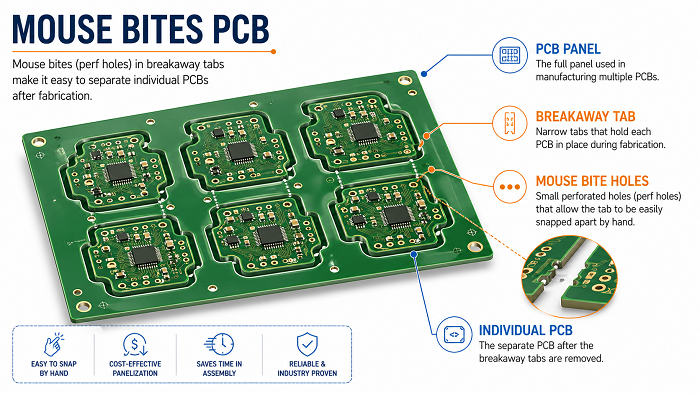
Mouse bites PCB refers to a PCB panelization method that uses small drilled holes on breakaway tabs to connect individual circuit boards inside a larger production panel. These small holes weaken the tab area, so the board can be separated more easily after fabrication, SMT assembly, inspection, or testing.

They are also called stamp holes, perforated tabs, breakaway holes, or PCB mouse bites. The name comes from the small semicircular marks left on the board edge after depaneling, which look similar to tiny bite marks.

In PCB manufacturing, most small boards are not always produced one by one. They are often placed into a larger panel to improve handling, assembly efficiency, and production stability. Mouse bites help keep each board connected during manufacturing while still allowing easy separation at the end.

This method is especially useful for:

  • Small PCB boards
  • Irregular-shaped PCBs
  • Round or curved PCB outlines
  • Boards with complex routing profiles
  • PCBs that cannot use straight V-cut lines
  • PCB panels that need strong temporary support during SMT assembly

For many projects, mouse bites are not just a small mechanical detail. They affect panel strength, edge quality, assembly stability, final appearance, and even product fit inside an enclosure.

Mouse Bites PCB Guide: Dimensions, V-Cut Comparison, and Design Tips

Why Are Mouse Bites Used in PCB Panelization?

Mouse bites are used because they allow several individual PCBs to stay connected in one larger panel during manufacturing and assembly. This improves production efficiency, protects small boards from handling damage, and makes SMT assembly more stable.

Main reasons to use mouse bites include:

  • They support small boards during automated assembly.
  • They allow irregular PCB shapes to be panelized.
  • They provide controlled breakaway points.
  • They help reduce manual handling during production.
  • They allow panel rails to be added for SMT machines.
  • They are suitable when V-cut is not possible.

For example, if a PCB has a round shape, a curved edge, or a special mechanical outline, V-cut may not work because V-cut requires straight lines. In this case, tab routing with mouse bites is often a better choice.

How Do PCB Mouse Bites Work?

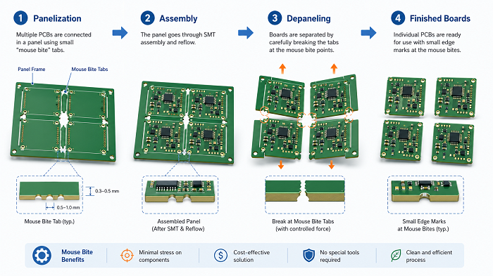
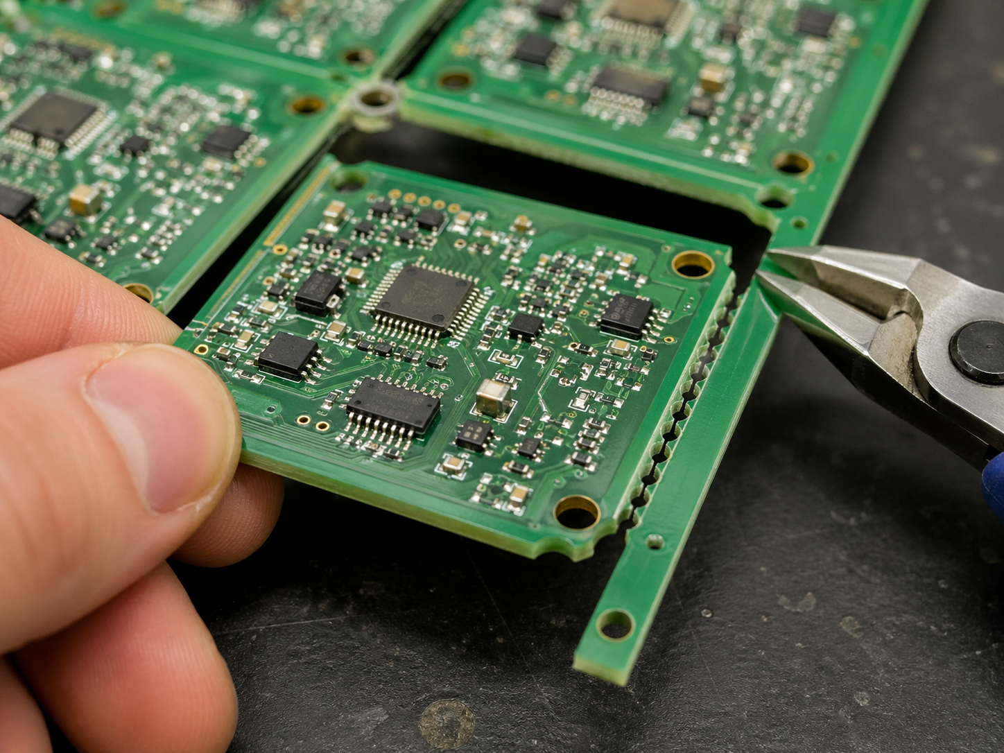
PCB mouse bites work by placing a row of small drilled holes through a breakaway tab. The tab holds the board in the production panel, while the holes reduce the mechanical strength of that tab. After assembly, the board can be snapped out along the weakened perforated area.

The process usually works like this:

How Do PCB Mouse Bites Work?

It looks easy, but it should pay much attention during the drilling process. If the holes are too large, the panel may become weak. If the holes are too small or too few, depaneling may become difficult. If the tab is placed near a connector, enclosure edge, or fragile component, separation stress may affect the final product.

A good mouse bite design balances three things:

  • Panel strength during manufacturing
  • Easy separation after assembly
  • Acceptable board edge quality after depaneling

What Are the Standard Mouse Bites PCB Dimensions?

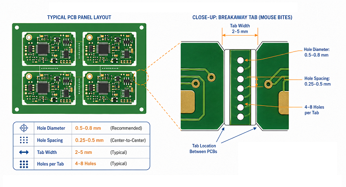
There is no single universal mouse bites PCB standard, because the best dimensions depend on board thickness, material, outline shape, component placement, panel size, and depaneling method. However, many PCB projects use small holes around 0.5 mm to 0.8 mm in diameter, with controlled spacing between holes.

What Are the Standard Mouse Bites PCB Dimensions?

The table below gives practical reference values commonly used in PCB panelization.

Design ItemCommon Reference RangePractical Design Note
Mouse bite hole diameter0.5–0.8 mmSmaller holes usually leave finer edge marks, but may require more holes
Hole spacing0.25–0.5 mm edge-to-edgeToo close may weaken the tab too much
Holes per tab4–8 holesDepends on tab width and board size
Tab width2–5 mmWider tabs improve panel strength but may need more cleanup
Tab quantity per board2–6 tabsLarger or heavier boards need more balanced support
Distance from componentsPreferably 2–3 mm or moreKeep away from brittle parts and solder joints
Board thickness consideration0.8–2.0 mm common rangeThicker boards may need adjusted tab design

A practical example:
For a small 1.6 mm FR4 PCB, a designer may use 0.5 mm mouse bite holes, 5 or 6 holes per tab, and 2 to 4 tabs around the board. If the board has connectors on one side, the tabs should be placed away from that connector edge to protect the mechanical fit.

The safest approach is to provide the PCB supplier with the mechanical requirements, especially if the board edge must fit into a plastic housing, guide rail, slot, or metal enclosure.

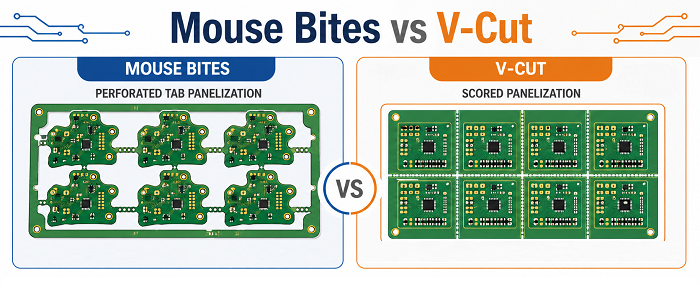
Mouse Bites vs V-Cut: Which PCB Depaneling Method Is Better?

Mouse bites are better for irregular-shaped, small, or routed PCB designs, while V-cut is usually better for rectangular boards with straight separation lines. The best choice depends on board shape, edge quality requirement, assembly method, and production volume.

V-cut, also called V-score, creates a straight groove on both sides of the PCB panel. The board is later separated along that scored line. It is efficient and clean for simple rectangular arrays. However, it does not work well for curved outlines or complex board shapes.

Mouse bites use routed outlines and perforated tabs, so they are much more flexible for non-rectangular PCB designs.

When Should You Choose Mouse Bites for PCB Panels?

You should choose mouse bites when the PCB shape is not suitable for V-cut, when the board is small and needs support during assembly, or when the panel requires routed outlines with controlled breakaway tabs.

Mouse bites are commonly used when the PCB has:

  • Irregular board outline
  • Round or curved edges
  • Small individual unit size
  • Complex mechanical profile
  • Nonlinear separation path
  • Panel rails for SMT assembly
  • Areas where V-cut cannot pass through
  • Connectors or shapes that break a straight-line panel layout

For example, many wearable devices, sensor modules, LED control boards, communication modules, and compact IoT products use non-standard board outlines. These designs often benefit from mouse bite panelization.

However, mouse bites should be used carefully if the PCB edge is part of the final product appearance. If the board will be visible to the user, inserted into a tight enclosure, or mounted along a precise mechanical edge, the tab position should be reviewed early.

If the product requires a very smooth edge, mouse bites can still be used, but the board may need sanding, trimming, or secondary routing after separation.

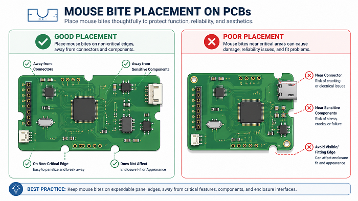
Where Should Mouse Bites Be Placed on a PCB?

Mouse bites should be placed on non-critical board edges, away from connectors, mounting features, fragile components, test points, and enclosure-fitting surfaces. Their position should support the panel during assembly while reducing stress during depaneling.

Placement is often more important than hole size. A technically correct mouse bite pattern can still cause problems if it is placed in the wrong area.

Where Should Mouse Bites Be Placed on a PCB?

Better locations include:

  • Non-visible edges
  • Non-mating edges
  • Areas without tight mechanical tolerance
  • Edges away from connectors
  • Areas with enough clearance from components
  • Symmetrical positions around the board

Avoid placing mouse bites near:

  • USB connectors
  • Board-to-board connectors
  • RF connectors
  • Mounting holes
  • Snap-fit housing edges
  • Gold fingers
  • Antenna keep-out areas
  • Ceramic capacitors close to the edge
  • BGA or fine-pitch ICs near the tab area
  • Test pads or fixture contact points

If a board has only one suitable edge for tabs, the panel design may need extra support rails. For larger boards, tabs should be distributed evenly to avoid twisting during reflow or depaneling.

What Problems Can Poor Mouse Bite Design Cause?

Poor mouse bite design can cause rough board edges, difficult depaneling, cracked corners, damaged solder joints, weak panels, SMT instability, and mechanical interference during final assembly.

Most mouse bite problems are preventable. They usually come from poor tab position, incorrect hole size, too few tabs, too many holes, or lack of communication between PCB design and manufacturing.

ProblemPossible CauseBetter Design Practice
Rough edge after separationHoles too large or tab placed on visible edgeMove tabs to non-critical edges or use cleanup routing
Board crackingTab too strong or too close to board cornerAdjust tab width and add clearance
Difficult depanelingToo few holes or holes too smallIncrease hole count or optimize spacing
Weak panel during SMTToo many holes or narrow tabsStrengthen tabs or add support rails
Component damageTab placed near fragile componentsMove tabs away from sensitive parts
Housing interferenceMouse bite burrs on fitting edgeAvoid tabs on enclosure-contact surfaces
Poor cosmetic appearanceTabs placed on visible edgePlace tabs on hidden or internal edges
Test fixture conflictTab blocks test accessReview test point and fixture layout early

The most common issue is edge roughness. Mouse bites naturally leave small marks because the board breaks along drilled perforations. This does not always affect electrical performance, but it can affect appearance, handling, and mechanical fit.

For consumer-facing products, medical device housings, handheld electronics, or precision-mounted assemblies, the edge requirement should be defined clearly before fabrication.

How Do Mouse Bites Affect PCB Assembly and Testing?

Mouse bites affect PCB assembly by controlling panel strength, board stability, depaneling stress, and handling efficiency. A good mouse bite layout helps the panel move smoothly through solder paste printing, pick-and-place, reflow soldering, AOI, X-ray inspection, ICT, and functional testing.

During SMT assembly, the PCB panel must stay flat and stable. If the tabs are too weak, the board may vibrate or move during handling. If the tabs are too strong, separation after assembly may require excessive force.

This is especially important for boards with:

  • Fine-pitch ICs
  • BGA packages
  • Ceramic capacitors
  • Tall connectors
  • Heavy components
  • Thin PCB materials
  • Edge-mounted components
  • High-density layouts

For assembled PCBs, depaneling should be done carefully. Snapping boards by hand may work for simple prototypes, but it can create mechanical stress on solder joints and components. For higher-value assemblies, controlled depaneling tools are safer.

How Do Mouse Bites Affect PCB Assembly and Testing?

How Can You Reduce Burrs After PCB Mouse Bite Depaneling?

You can reduce burrs after mouse bite depaneling by optimizing hole diameter, hole spacing, tab width, tab location, and post-processing method. The best strategy is to place mouse bites on non-critical edges and avoid using them on surfaces that require a smooth mechanical fit.

Mouse bite marks cannot always be completely avoided, but they can be controlled.

Practical ways to reduce burrs include:

  • Use smaller mouse bite holes when suitable.
  • Keep hole spacing consistent.
  • Avoid placing tabs on visible product edges.
  • Place the hole row closer to the waste side when possible.
  • Use proper depaneling tools instead of twisting the board by hand.
  • Add sanding or trimming after separation.
  • Use secondary routing for high-precision edges.
  • Choose V-cut if the board is rectangular and needs cleaner straight edges.

For boards that fit into housings, the safest approach is to mark the critical edges in the fabrication notes. A simple note such as “No mouse bites on enclosure-fitting edges” can prevent many mechanical problems.

How to Prepare Mouse Bites PCB Files for Manufacturing?

To prepare mouse bites PCB files for manufacturing, provide complete panelization details, board outline data, tab locations, hole sizes, rail requirements, tooling holes, fiducial marks, and any special edge-quality requirements.

Many PCB issues come from incomplete fabrication notes. A manufacturer can create panelization based on standard rules, but they may not know which edge is cosmetic, which edge fits into a housing, or which area must avoid mechanical stress.

Recommended file information includes:

  • Gerber files or ODB++ files
  • Board outline layer
  • Mechanical drawing or DXF file
  • PCB thickness
  • Surface finish requirement
  • Single board size
  • Finished panel size if required
  • Mouse bite tab locations
  • Hole diameter and hole spacing if specified
  • SMT rail width
  • Tooling holes
  • Fiducial mark positions
  • V-cut or routing instructions
  • Critical edge notes
  • Component keep-out areas near tabs
  • Test fixture requirements

For PCB assembly projects, panel design should be confirmed before SMT production. Once components are mounted, changing tab positions becomes much more difficult.

How to Choose the Right PCB Supplier for Mouse Bite Panelization?

Choose a PCB supplier that can review your panelization design, check mouse bite placement, understand SMT assembly requirements, and provide practical DFM feedback before production. Mouse bites look simple, but they affect both fabrication and assembly quality.

A reliable supplier should not only drill the holes. They should help confirm whether the tab locations are safe, whether the panel is strong enough, and whether the edge quality matches the final product requirement.

EBest PCB supports PCB fabrication, PCB panelization review, PCBA assembly, component sourcing, testing, and engineering support for prototype and production projects. If your design uses mouse bites, V-cut, routing, or special panel rails, sharing the mechanical requirements early can help improve manufacturing stability and final board quality.

FAQs About Mouse Bites PCB

1. What are mouse bites in PCB?

Mouse bites in PCB are small drilled holes placed on breakaway tabs in a PCB panel. They are commonly used in tab-routing panelization, especially for small or irregular-shaped PCBs. After depaneling, the remaining edge may show small rough marks where the tab was broken away.

2. Are mouse bites the same as stamp holes?

Yes. In many PCB manufacturing discussions, mouse bites are also called stamp holes, perforated holes, breakaway holes, or tab holes.

3. Do mouse bites leave rough PCB edges?

Yes, mouse bites can leave small burrs or serrated marks after the PCB is separated from the panel. This is normal because the board breaks along the perforated tab area.

4. What is the typical mouse bite hole size?

A common mouse bite hole size is around 0.5 mm to 0.8 mm in diameter. The exact size depends on PCB thickness, material, tab width, panel strength, and the supplier’s process capability.

5. Is mouse bite better than V-cut?

Mouse bite is better for irregular-shaped, round, small, or routed PCBs. V-cut is usually better for rectangular boards that can be separated along straight lines.

6. Can mouse bites be used for assembled PCBs?

Yes. Mouse bites are widely used for PCBs that go through SMT assembly in panel form. They help keep the boards connected and stable during production.

However, the tabs should be placed away from fragile components, connectors, test points, and precision mechanical edges. After assembly, controlled depaneling is preferred to reduce stress on solder joints and components.

7. How many mouse bite tabs does a PCB need?

The number of tabs depends on board size, shape, thickness, and assembly requirements. Small boards may use two to four tabs, while larger or heavier boards may need more support points.

Can mouse bites affect PCB cost?

Yes, mouse bites can affect PCB cost slightly because they usually require routing, drilled perforations, and more detailed panelization work. However, they can also improve assembly efficiency for small or irregular boards.

For simple rectangular boards, V-cut may be more cost-efficient. For complex shapes, mouse bites often provide better manufacturability and handling stability.

Conclusion

Mouse bites PCB is a practical panelization method for small, irregular, and routed circuit boards. It uses small drilled holes on breakaway tabs to hold PCBs in a manufacturing panel and make separation easier after fabrication or assembly.

The key to good mouse bite design is balance. The panel must be strong enough for SMT assembly, but the tabs must also be easy to remove without damaging the board. Hole size, hole spacing, tab width, tab quantity, and tab location all influence the final result.

For most projects, mouse bites are a strong choice when V-cut is not suitable. They offer flexibility, support complex PCB outlines, and help improve production handling. Still, designers should pay attention to edge quality, component clearance, enclosure fit, and depaneling stress.

If your PCB requires mouse bites, V-cut, routing, special panel rails, or PCBA assembly support, EBest PCB can help review the design before production and provide practical manufacturing suggestions.

For PCB fabrication and assembly inquiries, contact: sales@bestpcbs.com.

You may also like

Standard PCB Board Thickness: Complete Guide for 2-Layer, 4-Layer and 6-Layer PCBs

April 28th, 2026

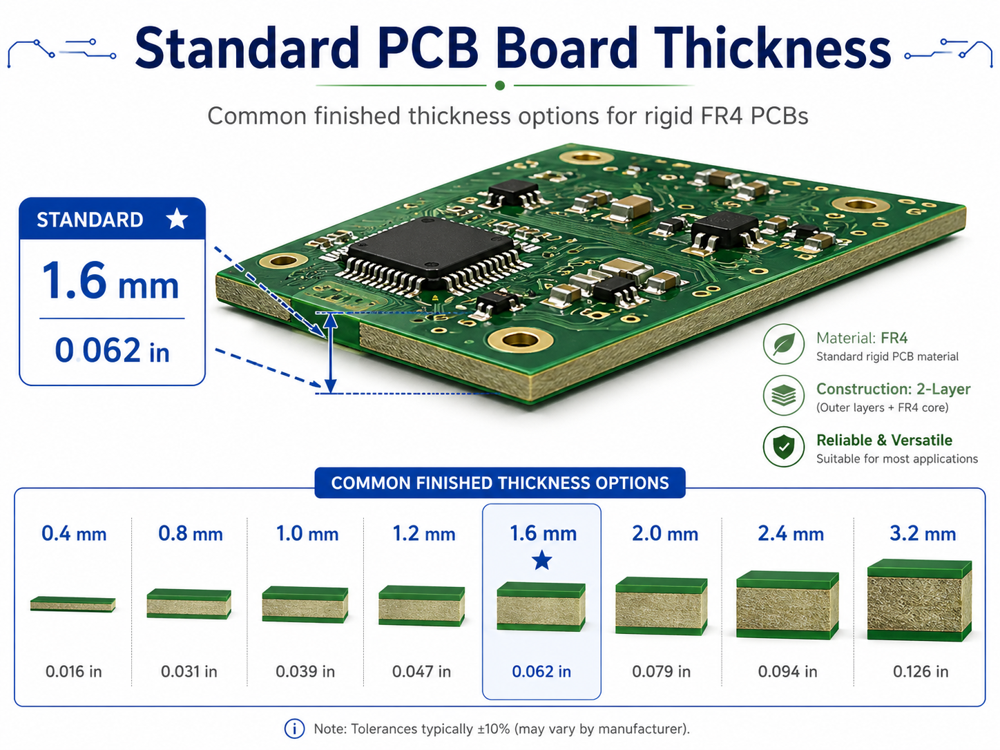
Standard PCB board thickness is commonly 1.6mm, also written as 1.57mm or 0.062 inch. This thickness is widely used for 2-layer, 4-layer, and many 6-layer FR4 PCBs because it provides a practical balance of mechanical strength, assembly compatibility, cost, and manufacturability.

However, PCB thickness can also range from 0.2mm to 3.2mm or more depending on product size, layer count, copper weight, impedance control, connector fit, and application requirements. For example, a wearable device may use a 0.6mm PCB, while an industrial power control board may use 2.0mm or 2.4mm for better rigidity.

Standard PCB Board Thickness: Complete Guide for 2-Layer, 4-Layer and 6-Layer PCBs

What Is the Standard PCB Board Thickness?

The standard PCB board thickness is usually 1.6mm, or about 0.062 inch. This is the most common finished thickness for rigid FR4 printed circuit boards used in industrial electronics, consumer products, control boards, communication devices, and general electronic assemblies.

In PCB manufacturing, “standard” does not mean every PCB must use this thickness. It means this value is widely available, easy to produce, compatible with many assembly processes, and accepted by most enclosure and connector designs.

Common PCB thickness options include:

PCB ThicknessInch EquivalentCommon Use
0.2mm0.008 inchUltra-thin rigid PCB, special compact devices
0.4mm0.016 inchThin electronics, compact modules
0.6mm0.024 inchSmall consumer devices, handheld products
0.8mm0.031 inchCompact control boards, plug-in modules
1.0mm0.039 inchSpace-limited electronics
1.2mm0.047 inchMedium-thin boards with better rigidity
1.6mm0.062 inchMost common standard PCB thickness
2.0mm0.079 inchIndustrial control, stronger mechanical demand
2.4mm0.094 inchHigh-strength PCB, larger boards
3.2mm0.126 inchHeavy-duty power boards, backplanes

For most standard FR4 boards, 1.6mm is a safe starting point. It is thick enough to resist bending in normal use, yet not so thick that it increases cost unnecessarily. It also works well with standard SMT assembly, through-hole components, mechanical supports, and many types of connectors.

Still, the best thickness should always match the product structure. A PCB for a small sensor cannot be selected the same way as a PCB for an inverter, a battery charger, or an automotive control module.

Why Is 1.6mm Considered the Standard PCB Thickness?

1.6mm became the most common PCB thickness because it offers a strong balance between strength, cost, and manufacturing convenience. It is thick enough for stable handling during fabrication and assembly, while still being economical for mass production.

For many engineers, 1.6mm is the default thickness unless there is a clear reason to change it.

You may keep 1.6mm when:

  • The PCB is a normal 2-layer or 4-layer FR4 board.
  • There is no strict enclosure height limit.
  • The board needs general mechanical strength.
  • The design uses common connectors or terminals.
  • The project is cost-sensitive.
  • There is no unusual impedance, bending, or thermal requirement.

You may choose another thickness when:

  • The product must be very thin.
  • The board must fit a special card-edge connector.
  • The enclosure has tight mechanical limits.
  • The PCB is large and needs more rigidity.
  • The circuit carries higher current.
  • The design needs a special impedance stackup.
  • The PCB is used in automotive, aerospace, medical, or harsh industrial environments.

So, 1.6mm is not a rule. It is a practical default.

How Thick Is a PCB Board in Common Applications?

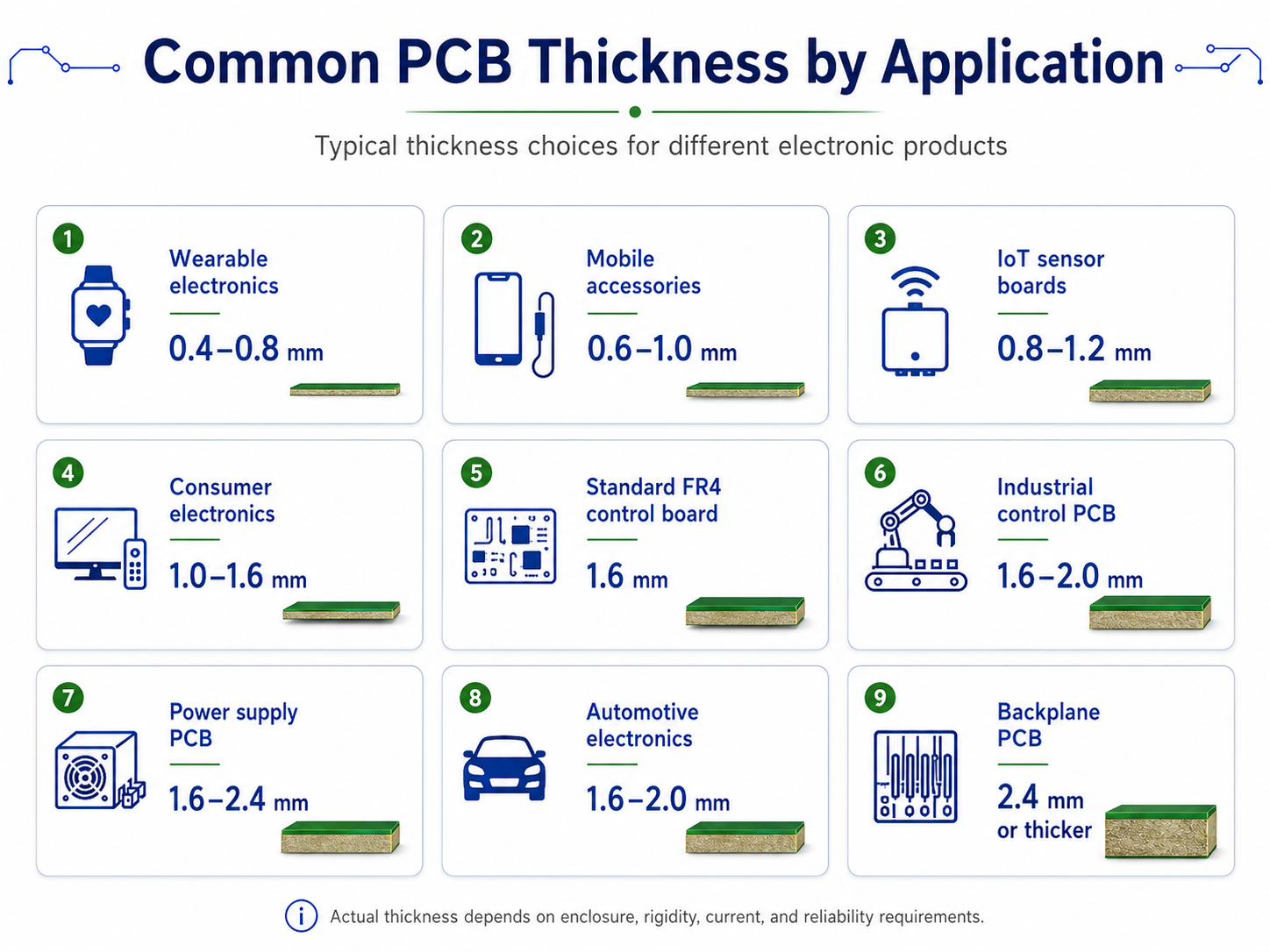
A PCB board can be as thin as 0.2mm or thicker than 3.2mm, depending on its application. The most common thickness for a general rigid PCB is 1.6mm, but thinner boards are popular in compact electronics, and thicker boards are used where strength, current capacity, or mechanical stability is important.

ApplicationCommon PCB ThicknessEngineering Reason
Wearable electronics0.4–0.8mmLightweight structure and thin product profile
Mobile accessories0.6–1.0mmCompact enclosure and lower weight
IoT sensor boards0.8–1.2mmSmall size with moderate rigidity
Consumer electronics1.0–1.6mmCost, strength, and assembly balance
Standard FR4 control board1.6mmMost common and economical option
LED control PCB1.0–1.6mmDepends on housing and current demand
Industrial control PCB1.6–2.0mmBetter strength and connector support
Power supply PCB1.6–2.4mmHigher current, larger components, better stability
Automotive electronics1.6–2.0mmVibration resistance and long-term durability
Backplane PCB2.4mm or thickerConnector force and structural support

For most projects, thickness selection starts with the mechanical design. The engineer should check the enclosure height, screw position, connector slot, component height, and assembly method first. After that, the electrical and thermal requirements should be reviewed.

A thin PCB can save space, but it may warp more easily during assembly. A thicker PCB improves rigidity, but it may increase cost and may not fit some connectors. A good PCB thickness decision balances both sides.

How Thick Is a PCB Board in Common Applications?

Standard PCB Thickness for 2-Layer Boards

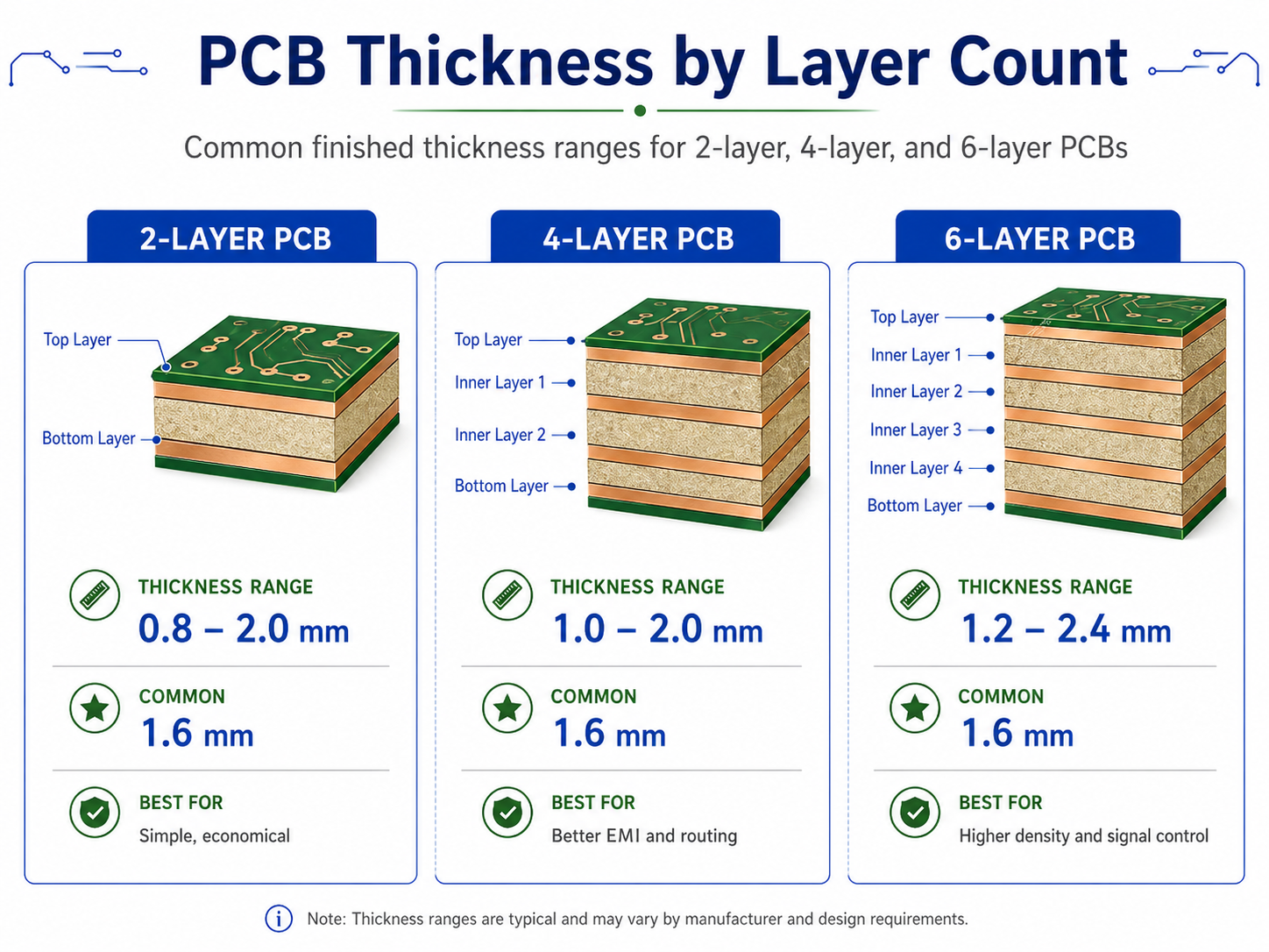
The standard PCB thickness for a 2-layer board is usually 1.6mm. This is the most common choice for general FR4 double-sided PCBs used in control circuits, LED products, power adapters, small instruments, test boards, and electronic modules.

A 2-layer PCB has copper on the top and bottom layers. The base material between them is usually FR4 core. Because the structure is simpler than a multilayer PCB, 2-layer boards are easier to manufacture and usually offer more flexible thickness choices.

Common 2-layer PCB thickness options include:

2-Layer PCB ThicknessTypical Use
0.4mmVery thin electronics, compact module boards
0.6mmSmall devices with limited space
0.8mmPlug-in modules, small control boards
1.0mmCompact products with better rigidity
1.2mmMedium-thin boards
1.6mmStandard 2-layer PCB thickness
2.0mmStronger industrial or power boards
2.4mm+Special mechanical or high-strength designs

For most 2-layer PCB designs, 1.6mm works well. It gives enough stiffness for manual handling, soldering, connector insertion, and screw mounting. It also helps reduce bending during wave soldering or reflow soldering.

However, if the board is part of a small product, such as a handheld sensor, remote controller, or compact communication module, 0.8mm or 1.0mm may be more suitable. If the board carries large terminals, relays, or heavy components, 2.0mm may be a stronger option.

The main point is simple: 2-layer does not automatically mean 1.6mm. The product structure decides the best thickness.

Standard PCB Thickness for 4-Layer Boards

The standard PCB thickness for a 4-layer board is also commonly 1.6mm. Many 4-layer FR4 PCBs use 1.6mm because it supports a stable stackup, good mechanical strength, and practical cost control.

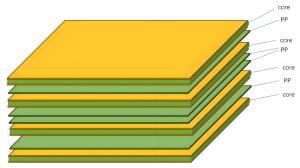
A 4-layer PCB usually has two outer copper layers and two inner copper layers. A common stackup may include:

  • Top signal layer
  • Inner ground layer
  • Inner power layer
  • Bottom signal layer

This structure improves routing density, EMI control, power distribution, and signal return path compared with a 2-layer board.

For 4-layer PCB thickness, the final value depends on:

  • Core thickness
  • Prepreg thickness
  • Copper weight
  • Inner layer copper
  • Outer layer copper plating
  • Solder mask thickness
  • Surface finish
  • Lamination pressure
  • Impedance requirements

This is why 4-layer PCB thickness should not be selected only by habit. If the board has USB, Ethernet, RF, DDR, LVDS, HDMI, or other high-speed signals, the stackup should be checked before production. In these cases, dielectric thickness between signal and reference plane may be more important than the total board thickness.

4-Layer PCB ThicknessSuitable Situation
0.8mmCompact electronics with controlled stackup
1.0mmThin multilayer modules
1.2mmSmaller boards with moderate rigidity
1.6mmMost common standard 4-layer PCB
2.0mmStronger board or special structure
2.4mmLarger PCB, connector-heavy design

For standard digital control boards, 1.6mm is usually practical. For compact devices, 1.0mm or 1.2mm may be better. For high-speed boards, the manufacturer should provide a stackup before fabrication.

Standard PCB Thickness for 6-Layer Boards

The standard PCB thickness for a 6-layer board is often 1.6mm, but 1.2mm, 2.0mm, and other custom thicknesses are also common depending on the design. A 6-layer PCB has more internal copper layers, so stackup planning becomes more important.

A 6-layer PCB may include signal layers, ground planes, power planes, and controlled impedance routing layers. Because more layers must fit into the same finished thickness, the manufacturer needs to carefully select core and prepreg materials.

A typical 6-layer board may use:

  • Top signal layer
  • Ground plane
  • Inner signal layer
  • Inner signal or power layer
  • Power or ground plane
  • Bottom signal layer

In many designs, the board can still be manufactured at 1.6mm. But the dielectric spacing, copper distribution, and lamination balance must be reviewed carefully. Poor layer balance may increase the risk of warpage, especially on larger boards.

What Is the Standard PCB Thickness for 6-Layer Boards?

What Is the Standard Thickness and Weight of a Copper Layer on a PCB?

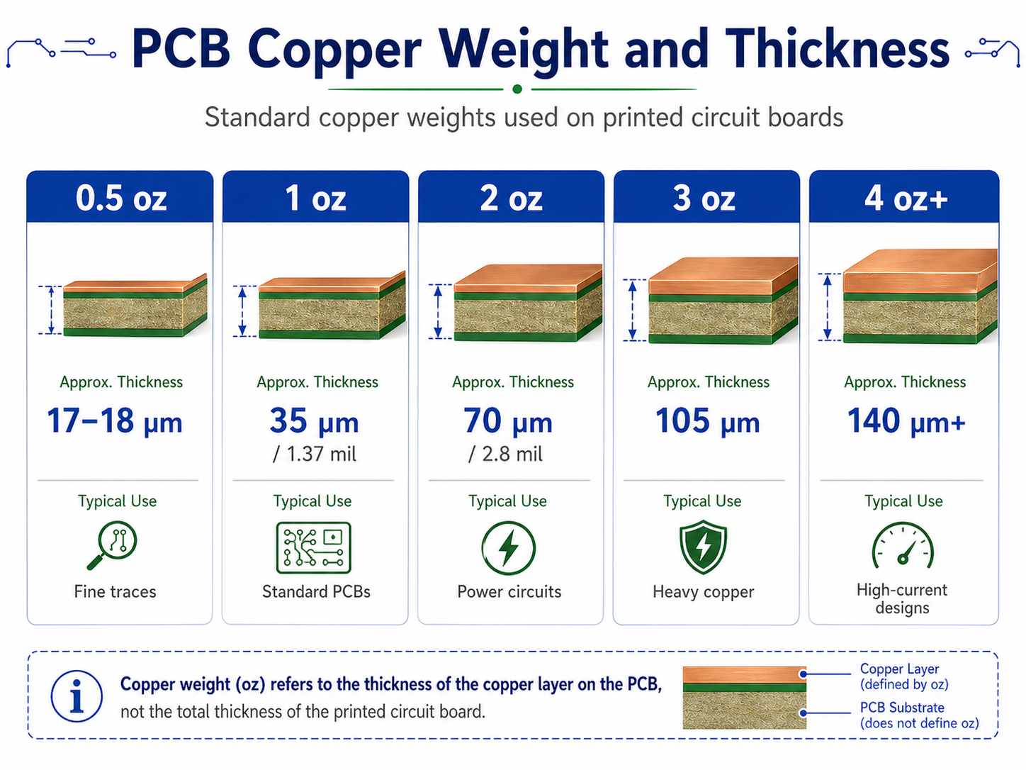
The standard copper thickness on a PCB is often 1 oz copper, which is about 35ÎŒm or 1.37 mil thick. Copper weight describes the copper thickness, not the total PCB thickness.

This is a common area of confusion. A 1.6mm PCB with 1 oz copper does not mean the whole board has 1 oz thickness. It means each specified copper layer uses copper foil with a weight of one ounce per square foot, which corresponds to around 35ÎŒm thickness before considering final plating effects.

What Is the Standard Thickness and Weight of a Copper Layer on a PCB?

Common PCB copper weights include:

Copper WeightApprox. Copper ThicknessTypical Application
0.5 oz17–18ÎŒmFine traces, compact signal boards
1 oz35ÎŒm / 1.37 milStandard PCB copper thickness
2 oz70ÎŒm / 2.8 milPower circuits, higher current paths
3 oz105ÎŒmHeavy copper PCB, motor control
4 oz+140ÎŒm+High-current and thermal applications

Copper weight affects current capacity, trace width, etching accuracy, thermal behavior, and cost. A board with thicker copper can carry more current, but it also requires wider spacing and more careful manufacturing control.

For example, a power supply PCB may use 2 oz copper to handle higher current. A fine-pitch signal board may use 0.5 oz or 1 oz copper to support narrow traces and small spacing. A heavy copper PCB may use 3 oz or more for power conversion, battery systems, industrial equipment, and motor drives.

For multilayer PCBs, inner copper and outer copper may also be different. Outer layers usually gain additional copper thickness during plating, while inner layers remain closer to the original copper foil thickness. This should be considered when calculating current capacity and impedance.

How Does PCB Thickness Tolerance Affect Your Design?

PCB thickness tolerance is the allowed difference between the specified board thickness and the actual finished thickness. For example, a PCB ordered as 1.6mm may not measure exactly 1.600mm after fabrication. A reasonable manufacturing tolerance must be expected.

Thickness tolerance matters because PCB fabrication includes lamination, copper plating, solder mask coating, surface finish, and final routing. These processes all introduce small variations.

For ordinary control boards, standard tolerance is often acceptable. For card-edge products, backplanes, connectors, press-fit assemblies, or controlled-impedance boards, the tolerance should be defined clearly in the drawing or fabrication notes.

For example:

Finished PCB thickness: 1.6mm ±10%, FR4, 1 oz outer copper, ENIG surface finish, impedance control required.

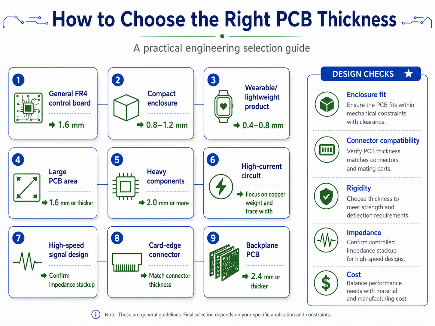
How Do You Choose the Right PCB Thickness for Your Project?

To choose the right PCB thickness, start with mechanical requirements first, then review electrical, thermal, and manufacturing needs. A good PCB thickness should fit the product, support the components, meet electrical performance, and remain manufacturable at a reasonable cost.

Here is a practical selection guide:

Design RequirementRecommended Direction
General FR4 control boardUse 1.6mm
Cost-sensitive prototypeUse standard 1.6mm when possible
Compact enclosureConsider 0.8mm, 1.0mm, or 1.2mm
Wearable or lightweight productConsider 0.4mm to 0.8mm
Large PCB areaUse 1.6mm or thicker to reduce bending
Heavy componentsConsider 2.0mm or stronger mechanical support
High-current circuitFocus on copper weight and trace width
High-speed signal designConfirm impedance stackup before fabrication
Card-edge connectorMatch the connector thickness requirement
Industrial environmentConsider 1.6mm, 2.0mm, or thicker
Automotive applicationCheck vibration, thermal, and reliability needs
Backplane PCBConsider 2.4mm or thicker

A simple rule can help:

  • Use 1.6mm for standard designs.
  • Use 0.8mm–1.2mm for compact electronics.
  • Use 2.0mm or thicker for high-strength or heavy-component boards.
  • Use a custom stackup when impedance, RF, thermal, or mechanical requirements are strict.

Thickness should also be discussed early with the PCB manufacturer. If the design uses special materials, controlled impedance, buried vias, blind vias, heavy copper, or HDI structures, the stackup should be confirmed before layout is finalized.

How Do You Choose the Right PCB Thickness for Your Project?

Can a PCB Thickness Calculator Give the Final Board Thickness?

A PCB thickness calculator can provide a useful estimate, but it cannot always give the final finished PCB thickness. Final thickness depends on actual laminate materials, prepreg flow, copper thickness, lamination pressure, solder mask, plating, surface finish, and manufacturing tolerance.

A calculator is helpful when you need early-stage estimation. For example, it can help you understand how core thickness, prepreg thickness, and copper layers may build up into the final board thickness. It can also support early stackup planning for 4-layer or 6-layer PCBs.

However, a calculator should not replace the manufacturer’s stackup confirmation.

This is especially true for:

  • Impedance-controlled PCB
  • High-speed digital PCB
  • RF PCB
  • HDI PCB
  • Heavy copper PCB
  • Rigid-flex PCB
  • Automotive PCB
  • Medical electronics PCB
  • Aerospace PCB

For standard 2-layer FR4 boards, the thickness is usually easier to predict. For multilayer boards, the actual lamination result is more complex. Prepreg may compress during lamination, resin may flow into copper gaps, and copper distribution may influence final thickness.

The safest process is:

  1. Choose a target finished thickness.
  2. Define copper weight.
  3. Define layer count.
  4. Share impedance requirements if any.
  5. Ask the PCB manufacturer to provide a stackup.
  6. Review the stackup before final layout.
  7. Confirm tolerance before mass production.

A PCB thickness calculator is a planning tool. The approved manufacturing stackup is the production reference.

What PCB Board Sizes and Thicknesses Are Commonly Available?

Standard PCB board sizes do not mean every PCB has one fixed size. In PCB manufacturing, board size is usually customized according to the customer’s Gerber files. What manufacturers often standardize are material panel sizes, laminate thicknesses, copper weights, and production capability ranges.

For most FR4 PCBs, common finished thicknesses include:

Common Finished ThicknessTypical Availability
0.4mmAvailable for thin rigid PCB
0.6mmCommon for compact products
0.8mmCommon for small modules
1.0mmCommon for thin electronic products
1.2mmCommon for medium-thin PCB
1.6mmMost standard PCB board thickness
2.0mmCommon for industrial boards
2.4mmAvailable for stronger structures
3.2mmUsed for special heavy-duty boards

Board size also affects thickness choice. A small PCB can use thinner material more easily because it has less bending area. A large PCB may need 1.6mm or thicker material to reduce flexing during assembly and field use.

For example, a 30mm × 50mm sensor PCB can often use 0.8mm without major mechanical concerns. A 250mm × 180mm industrial control PCB may need 1.6mm or 2.0mm to remain stable. A backplane with multiple connectors may need even greater thickness.

How Does PCB Thickness Affect Cost and Lead Time?

PCB thickness affects cost and lead time mainly through material availability, lamination complexity, copper weight, and special processing requirements. Standard 1.6mm FR4 boards are usually easier to manufacture quickly because materials are widely available and production processes are mature.

Cost usually increases when:

  • Thickness is non-standard.
  • Material is not commonly stocked.
  • Copper weight is heavy.
  • Layer count is high.
  • Impedance control is required.
  • Tolerance is very tight.
  • The board is very thin and large.
  • The board is thick with small drilled holes.

For cost-sensitive designs, use common FR4 thickness and standard copper weight whenever possible. For performance-critical products, choose thickness based on engineering needs first, then optimize cost with the manufacturer.

How Should You Specify PCB Thickness in Fabrication Files?

You should specify PCB thickness as a finished board thickness, not only as a material preference. The fabrication drawing should include finished thickness, tolerance, copper weight, layer count, material type, surface finish, and any controlled impedance requirement.

A clear fabrication note helps prevent misunderstanding between the designer, buyer, and PCB manufacturer.

A basic example:

Material: FR4, finished thickness 1.6mm ±10%, 2 layers, 1 oz finished copper, green solder mask, white silkscreen, HASL lead-free finish.

A more advanced example:

Material: High Tg FR4, 4-layer PCB, finished thickness 1.6mm ±0.16mm, outer copper 1 oz finished, inner copper 0.5 oz, ENIG surface finish, controlled impedance required according to approved stackup.

For a high-speed PCB, the stackup document should be treated as part of the design. It should define each copper layer, dielectric layer, material type, dielectric thickness, copper weight, and target impedance.

Good communication at this stage can greatly reduce sample issues and improves production consistency.

FAQs About Standard PCB Board Thickness

1. What is the most common standard PCB board thickness?
The most common standard PCB board thickness is 1.6mm, also written as 1.57mm or 0.062 inch. It is widely used for FR4 2-layer, 4-layer, and many 6-layer PCB designs because it offers good strength, stable manufacturing, and broad assembly compatibility.

2. Is 1.6mm PCB thickness required for all PCB designs?
No, 1.6mm is common but not required for all designs. Thin products may use 0.4mm, 0.6mm, 0.8mm, or 1.0mm, while industrial control boards, power electronics, and backplanes may use 2.0mm, 2.4mm, or thicker boards.

3. What is the standard PCB thickness for a 2-layer board?
The standard PCB thickness for a 2-layer board is usually 1.6mm. However, 0.8mm and 1.0mm are also common for compact electronics, while 2.0mm may be used when the board needs stronger mechanical support.

4. Can I use a PCB thickness calculator for final production?
A PCB thickness calculator is useful for early estimation, but it should not be the only reference for final production. The final board thickness should be confirmed by the PCB manufacturer through an approved stackup and fabrication specification.

If your PCB project requires controlled thickness, special copper weight, impedance stackup, or manufacturability review, you can send your Gerber files, BOM, and technical requirements to EBest PCB for engineering support.

Contact: sales@bestpcbs.com

You may also like

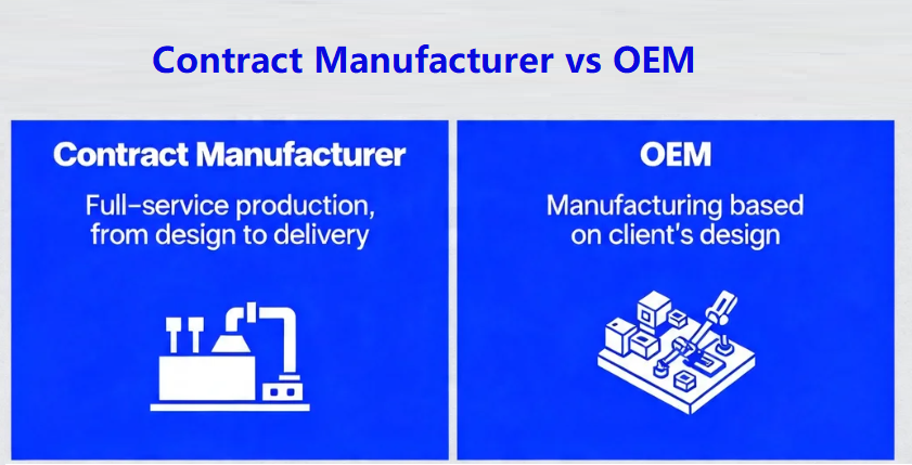
What are Contract Manufacturer vs OEM Differences?

April 16th, 2026

When companies develop a new product, they often compare contract manufacturer vs OEM differences before choosing a production model. These two terms are related, but they are not the same. The choice affects product control, cost, speed, and supply chain strategy.

In electronics, this decision matters even more because production often includes PCB fabrication, component sourcing, assembly, testing, and final integration. A clear understanding of contract manufacturing vs OEM differences helps companies choose the right path and avoid confusion later.

Contract Manufacturer vs OEM Differences

What Does OEM Mean in Manufacturing?

OEM stands for Original Equipment Manufacturer. An OEM produces parts or products that are used in another company’s final product. The brand owner usually controls the design, specifications, and branding.

In simple terms, an OEM builds what you design.

For example, a company may design a medical device but rely on an OEM to produce key components. The final product is sold under the brand owner’s name, not the OEM’s.

OEM relationships often focus on:

  • Strict design ownership
  • Brand control
  • Long-term supply agreements
  • High consistency in production

OEMs follow detailed instructions. They rarely make design changes unless requested. This makes them ideal for businesses that want full control over their product.

What Does OEM Mean in Manufacturing?

What Is a Contract Manufacturer and How Does It Work?

A contract manufacturer provides full production services for a client. This includes sourcing materials, assembling products, testing, and even packaging.

Unlike OEMs, contract manufacturers often support the entire production lifecycle. Here is how it usually works:

1. You provide product requirements or a design concept

2. The contract manufacturer reviews and optimizes it

3. They source components and manage production

4. They handle testing and quality control

5. Finished goods are delivered to you

This model reduces operational burden. You focus on marketing and sales while the manufacturer handles production.

Contract manufacturers are flexible. They can support low-volume prototyping and large-scale production.

Contract Manufacturer

Contract Manufacturer

Is a Contract Manufacturer the Same as OEM?

No, they are not the same. While both produce goods, their roles differ in scope and responsibility.

An OEM focuses on manufacturing based on your design. A contract manufacturer offers a broader service that may include design support, sourcing, and logistics.

The difference lies in involvement.

  • OEM = Build exactly what you specify
  • Contract manufacturer = Support and produce your product

Some companies use both models at different stages. For example, they may start with a contract manufacturer for development, then move to an OEM for mass production.

What Are the Key Differences Between OEM and Contract Manufacturing?

Understanding the differences helps you choose the right partner. The table below highlights the main contrasts:

AspectOEMContract Manufacturer
Core RoleManufacturing onlyFull-service production partner
Design ResponsibilityClient-ownedShared or supported
FlexibilityLimitedHigh
Engineering SupportMinimalStrong
Supply ChainManaged by clientManaged by manufacturer
Time to MarketSlower if unpreparedFaster with support
Cost StructureLower unit cost at scaleIncludes service value
ScalabilityStrong for large volumesStrong for both small and large volumes

OEM focuses on execution, while contract manufacturing focuses on solutions.

Which Is Better: OEM or Contract Manufacturing for Your Business?

There is no single answer, the best choice depends on your business model, resources, and goals.

OEM is often the better choice when:

  • Your product design is fully finalized
  • You want strict control over every detail
  • You have an experienced sourcing team
  • You are producing at high volume

Contract manufacturing is often better when:

  • Your design is still evolving
  • You need engineering support
  • You want faster product launch
  • You lack internal manufacturing expertise

Startups and small teams often benefit from contract manufacturers. They reduce complexity and speed up development.

How Do Costs Compare Between OEM and Contract Manufacturing?

OEM manufacturing often offers lower per-unit cost, especially at high volumes. However, you must manage several additional areas:

  • Supplier selection
  • Component procurement
  • Inventory management
  • Quality assurance
  • Logistics coordination

Contract manufacturers include many of these services in their pricing. This may increase the upfront cost, but it reduces internal workload.

A simple way to compare:

  • OEM: Lower visible cost, higher hidden effort
  • Contract manufacturing: Higher upfront cost, lower operational burden

For many companies, the total cost becomes similar when all factors are considered.

What Are the Risks of OEM vs Contract Manufacturing?

OEM risks include:

  • Limited flexibility for design changes
  • Dependence on accurate documentation
  • Responsibility for supply chain issues
  • Longer adjustment cycles

Contract manufacturing risks include:

  • Less direct control over certain processes
  • Dependence on one supplier
  • Potential variation in service quality

These risks can be reduced through clear contracts, regular communication, and strong quality systems.

When Should You Choose a Contract Manufacturer Instead of an OEM?

There are situations where contract manufacturing clearly stands out. You should consider this model when:

  • You are launching a new product
  • Your design is not fully optimized
  • You need quick prototyping
  • Your team lacks manufacturing experience
  • You want to shorten time to market
  • You need flexibility in production volume

Contract manufacturers help reduce trial-and-error, they can guide you through early challenges and improve product readiness.

How Does EMS Fit Into OEM and Contract Manufacturing?

EMS stands for Electronics Manufacturing Services. It is a specialized segment of contract manufacturing focused on electronic products.

EMS providers offer services such as:

  • PCB assembly
  • Component sourcing
  • Functional testing
  • Final product assembly

They work closely with both OEMs and product companies.

In a typical setup:

  • A brand designs the product
  • An EMS provider manufactures and assembles it

EMS providers combine technical expertise with production capability. They play a key role in industries where precision and reliability are critical.

What Industries Prefer OEM vs Contract Manufacturing?

Different industries choose different models based on their needs. Industries that often prefer OEM include:

  • Automotive manufacturing
  • Aerospace systems
  • Heavy industrial equipment

These sectors require strict control, long product lifecycles, and stable designs.

Industries that often prefer contract manufacturing include:

  • Consumer electronics
  • Medical devices
  • Smart home and IoT products

These industries move quickly, they require flexibility, fast updates, and efficient scaling.

Some companies use both models within the same product line. They adjust based on product maturity and market demand.

What Industries Prefer OEM vs Contract Manufacturing?

Why Choose EBest Circuit (Best Technology) as Your Contract Manufacturer?

When selecting a contract manufacturer, technical capability alone is not enough. Reliability, responsiveness, and engineering support matter equally. Our key advantages including:

  • 20+ years of PCBA experience
  • One-stop service: PCB → Components → Assembly → Box build
  • 1+3 engineering support model
  • No MOQ for prototypes and small batches
  • Fast delivery: ~1.5 weeks PCBA turnaround
  • Full traceability system (5-second tracking)
  • Certified: ISO9001, ISO13485, IATF16949, AS9100D, UL

Clients also benefit from:

  • Quick response times for inquiries and updates
  • Transparent pricing and cost control
  • Scalable solutions that grow with your business

With a practical approach and strong technical foundation, EBest Circuit supports companies at every stage of product development.

FAQs

1. Can a company provide both OEM and contract manufacturing services?

    Yes, some manufacturers offer both models. They may produce their own products while also manufacturing custom designs for clients.

    2. Which model gives better control over product quality?

    Contract manufacturing offers more control because the client defines specifications, materials, and testing standards.

    3. Is contract manufacturing suitable for startups?

    Yes, it allows startups to bring products to market without investing in expensive production facilities.

    4. Does OEM always mean faster production?

    OEM can be faster for standard products, but it may not be flexible for custom requirements.

    5. What should I look for in a manufacturing partner?

    Key factors include experience, quality systems, communication, and the ability to scale production.

    If you are planning your next project or exploring production options, feel free to reach out for professional support: sales@bestpcbs.com

    You may also like

    PCB Design for LED Light: Ultimate Guide to High-Performance, Reliable Lighting PCBs

    April 7th, 2026

    When it comes to PCB design for LED light, every detail—from thermal management to component layout—determines the performance, reliability, and lifespan of your LED products. Whether you’re designing for medical devices, aerospace lighting, or industrial equipment, getting PCB design for LED light right is non-negotiable. If you’re searching for a trusted PCB design for LED light manufacturer, look no further than EBestpcb. We deliver tailored solutions that solve your biggest design and production challenges, backed by expertise, certifications, and a proven track record in critical industries.

    PCB Design for LED Light

    Why Choose EBestpcb for Your PCB Design for LED Light Needs?

    • Delivery Time: We prioritize fast, reliable lead times without compromising quality, ensuring your LED PCB projects stay on schedule—even for tight deadlines and complex designs.
    • Quality Assurance: Our PCB design for LED light solutions undergo rigorous testing (including thermal cycling, AOI, and X-ray inspection) to ensure consistency, durability, and compliance with industry standards.
    • Certifications: We hold global certifications that validate our commitment to excellence, including ISO 9001, ISO 13485 (for medical applications), IPC-A-610, and RoHS compliance.
    • Cost-Effective Support: Enjoy free DFM (Design for Manufacturability) analysis to optimize your PCB design for LED light and reduce production issues, plus flexible low MOQ for prototyping and small-batch orders.
    • Comprehensive Service: Our team of engineers provides end-to-end support—from initial design consultation and prototype development to mass production and post-delivery assistance.

    Our PCB Design for LED Light Services

    • Custom PCB design for LED light (single-layer, double-layer, and multi-layer PCBs) tailored to your specific LED application and industry requirements.
    • Free DFM analysis to identify design flaws, optimize thermal performance, and ensure manufacturability for LED PCBs.
    • Prototype development and testing for PCB design for LED light, including thermal testing, brightness consistency checks, and EMC compliance verification.
    • Mass production of LED PCBs with strict quality control, including AOI, X-ray, and functional testing to guarantee reliability.
    • Post-production support, including troubleshooting, design revisions, and technical guidance for LED PCB integration.
    • Specialized solutions for high-power LED PCBs, medical LED devices, aerospace lighting, and industrial LED equipment.

    Our Certifications for PCB Design for LED Light

    • ISO 9001:2015 – Quality management system certification, ensuring consistent quality across all PCB design for LED light projects.
    • ISO 13485:2016 – Certification for medical device components, validating our ability to design and manufacture LED PCBs for medical applications (e.g., surgical lighting, patient monitors).
    • IPC-A-610 – Acceptability of Electronic Assemblies, ensuring our LED PCBs meet the highest industry standards for soldering and component placement.
    • RoHS & REACH Compliance – Our PCB design for LED light solutions are free of hazardous substances, making them suitable for global markets.
    • UL Certification – For LED PCBs used in commercial and industrial applications, ensuring safety and compliance with electrical standards.

    Our Manufacturing Capabilities for PCB Design for LED Light

    CapabilitySpecificationsApplicable LED PCB Types
    Layer Count1-24 layersAll LED PCBs (low-power to high-power, medical, aerospace)
    Copper Thickness0.5oz – 10oz (standard 2oz for high-power LED PCBs)High-power LED PCBs, industrial LED equipment
    Board Thickness0.2mm – 3.0mmMedical LED devices, aerospace lighting, compact LED modules
    Surface FinishImmersion Gold, HASL (Lead-Free), OSP, ENIGAll LED PCBs (critical for solderability and corrosion resistance)
    Minimum Line Width/Spacing3mil/3milHigh-density LED PCBs, medical and aerospace applications
    Testing CapabilitiesAOI, X-ray, Thermal Cycling (-40℃~125℃), EMC TestingAll LED PCBs (ensures reliability and compliance)

    Why Do LED PCB Designs Fail? We Solve Your Biggest Pain Points

    Every PCB design for LED light project faces unique challenges—from overheating and brightness inconsistency to poor manufacturability and compliance issues. We’ve helped hundreds of clients overcome these pain points with tailored solutions, and we’re ready to help you too. Choose EBestpcb for PCB design for LED light that delivers reliability, performance, and peace of mind.

    Pain Point 1: Overheating LED PCBs Leading to Premature Failure

    Overheating is the #1 cause of LED PCB failure. LED chips generate significant heat, and poor thermal management in PCB design for LED light leads to high junction temperatures, faster light degradation, and component failure. Our solution: We integrate thermal-electric separation structures, high-thermal-conductivity materials (copper, ceramic substrates), and optimized thermal vias to reduce junction temperatures by 5-15℃, extending LED lifespan by up to 50%.

    Pain Point 2: Brightness Inconsistency and Color Drift

    Many LED PCBs suffer from uneven brightness or color drift, often due to poor current distribution or inadequate PCB layout. Our solution: We design PCB design for LED light with star-shaped power supply and grounding, independent constant current drivers (±3% precision), and optimized trace widths to ensure uniform current flow. For RGBW LED PCBs, we implement separate current control for each color channel to maintain color consistency.

    Pain Point 3: Design Flaws Causing Manufacturability Issues

    Even the best PCB design for LED light fails if it’s not manufacturable. Common issues include incorrect pad sizes, insufficient spacing, and poor thermal via placement. Our solution: We provide free DFM analysis to identify and fix these flaws early, ensuring your LED PCB design is optimized for our manufacturing processes—reducing rework, delays, and inconsistencies.

    Pain Point 4: Non-Compliance with Industry Standards

    Medical, aerospace, and industrial LED applications require strict compliance with industry standards (ISO 13485, IPC-A-610). Our solution: All our PCB design for LED light projects are developed in compliance with relevant standards, and we conduct rigorous testing to ensure your LED PCBs meet the requirements for your industry—whether it’s medical device safety or aerospace reliability.

    What Is the Best PCB Material for LED Light Design?

    The best PCB material for PCB design for LED light depends on your application, power requirements, and environment. Below is a comparison of the most common materials to help you choose:

    PCB MaterialThermal ConductivityKey AdvantagesBest For
    FR-40.3-0.5 W/m·KCost-effective, versatile, easy to manufactureLow-power LED lights (e.g., household lighting)
    Aluminum PCB1-2 W/m·KLightweight, good thermal dissipation, cost-effectiveCommercial LED lights, industrial equipment lighting
    Copper PCB3-4 W/m·KExcellent thermal conductivity, high reliabilityHigh-power LED lights (e.g., stage lights, industrial high-bay lights)
    Ceramic (AlN)150-200 W/m·KUltra-high thermal conductivity, high insulationMedical LED devices, aerospace lighting, precision optical LEDs

    How to Optimize Thermal Management for PCB Design for LED Light?

    Thermal management is critical for PCB design for LED light—it directly impacts LED lifespan and performance. Follow these steps to optimize thermal management:

    1. Choose the Right Substrate Material

    For high-power LED PCBs, use copper or ceramic substrates (instead of FR-4) to improve heat dissipation. Ceramic substrates are ideal for medical and aerospace applications where reliability is critical.

    2. Optimize Pad and Trace Design

    Enlarge LED pads and use 2oz+ copper thickness to increase heat transfer. Add thermal vias (0.3mm diameter, 1.5mm spacing) under LED chips to channel heat to the back of the PCB.

    3. Implement Thermal-Electric Separation Structures

    For high-power applications, use thermal-electric separation PCBs to separate the circuit layer from the heat dissipation layer—reducing thermal resistance and preventing signal interference.

    4. Add Heat Sinks or Thermal Pads

    For extreme heat applications (e.g., industrial high-bay lights), integrate heat sinks or thermal pads to further reduce junction temperatures. Use thermal adhesive (Tg ≄ 150℃) for optimal heat transfer.

    PCB Design for LED Light: Industry Case Studies

    Medical Industry: Surgical LED Lighting PCB

    A medical device manufacturer needed a PCB design for LED light for surgical lighting—requiring high brightness, low heat, and ISO 13485 compliance. We designed a 4-layer ceramic PCB with a thermal-electric separation structure, 3oz copper, and strict ESD protection. The result: LED junction temperature reduced by 12℃, brightness consistency improved by 95%, and full compliance with medical standards.

    Aerospace Industry: Aircraft Cabin LED Lighting PCB

    An aerospace client needed a lightweight, durable PCB design for LED light for aircraft cabin lighting. We used an aluminum substrate with an optimized trace layout, RoHS-compliant materials, and thermal cycling testing (-40℃~125℃). The PCB withstood 1000+ thermal cycles with no performance degradation, meeting aerospace reliability requirements.

    Industrial Equipment: High-Power LED Industrial Light PCB

    An industrial client required a PCB design for LED light for high-bay industrial lighting (100W+). We designed a copper substrate PCB with thermal vias, constant current drivers, and PWM dimming (2kHz+ to avoid flicker). The PCB achieved 85% power efficiency, reduced heat buildup by 30%, and lasted 50,000+ hours of continuous use.

    FAQ: Common Questions About PCB Design for LED Light

    1. What Causes LED PCB Overheating, and How to Fix It?

    LED PCB overheating is caused by poor thermal management, inadequate copper thickness, or incorrect substrate material. To fix it: use high-thermal-conductivity substrates (copper/ceramic), add thermal vias, enlarge LED pads, and integrate heat sinks. Our PCB design for LED light team optimizes all these factors to keep junction temperatures within safe limits.

    2. How to Ensure Brightness Consistency in LED PCB Design?

    Brightness inconsistency stems from uneven current distribution. Fix it by using star-shaped power supply/grounding, independent constant current drivers for each LED or color channel, and optimized trace widths. We implement these strategies in every PCB design for LED light to ensure uniform brightness.

    3. Which PCB Layer Count Is Best for LED Light Design?

    The best layer count depends on your LED application. Low-power LED lights (household) use 1-2 layers. High-power, complex LED lights (medical/aerospace) use 4-8 layers to separate power, signal, and thermal layers. We recommend 4 layers for most industrial and medical PCB design for LED light projects for optimal performance.

    4. Do LED PCBs Need ESD Protection, and Why?

    Yes, LED PCBs need ESD protection. Static discharge can damage LED chips (hard or soft failure), leading to premature failure. We add TVS diodes and ESD protection circuits to all PCB design for LED light projects, especially for medical and aerospace applications where reliability is critical.

    5. How to Optimize PCB Design for LED Light Manufacturability?

    Optimize manufacturability by following DFM guidelines: use standard pad sizes, ensure adequate trace spacing (≄3mil), place thermal vias correctly, and avoid complex layouts. Our free DFM analysis for PCB design for LED light identifies and fixes manufacturability issues early, reducing rework and delays.

    6. What Certifications Are Required for Medical LED PCB Design?

    Medical LED PCB design requires ISO 13485 certification (for medical devices), IPC-A-610 (for electronic assemblies), and RoHS compliance. We ensure all our medical PCB design for LED light projects meet these certifications, plus any additional client-specific requirements.

    Choose EBestpcb for Your PCB Design for LED Light Needs

    Whether you’re designing LED PCBs for medical devices, aerospace lighting, or industrial equipment, EBestpcb is your trusted partner for high-quality, reliable PCB design for LED light solutions. We solve your biggest pain points, deliver on time, and ensure compliance with industry standards. If you need PCB design for LED light that combines performance, durability, and manufacturability, contact us today—we’re ready to bring your project to life.

    You may also like

    Copper & Aluminum Busbar Ampacity, Sizing & Calculation Guide

    April 7th, 2026

    Key Takeaways

    • Busbar ampacity is the maximum continuous current a busbar can carry under specified installation and temperature conditions.
    • Copper busbars offer higher electrical conductivity and generally require smaller cross-sections than aluminum for comparable resistance.
    • Busbar sizing calculations begin with current, conductor area, and current density, followed by thermal and short-circuit verification.
    • Temperature rise, ventilation, installation orientation, and joint resistance can substantially change actual current-carrying capacity.
    • Busbar ampacity charts are useful for preliminary selection, but final ratings must reflect the actual equipment configuration.

    Busbar ampacity determines how much electrical current a copper or aluminum busbar can safely carry without exceeding its allowable operating temperature. The correct busbar size depends on conductor material, cross-sectional area, ambient temperature, ventilation, installation method, and electrical loading.

    For engineers designing power distribution systems, battery connections, industrial equipment, or high-current PCB assemblies, selecting a busbar involves more than matching its dimensions to a current rating. This guide explains the calculation formulas, copper and aluminum differences, practical sizing examples, and verification methods needed to select an appropriate conductor.

    Copper & Aluminum Busbar Ampacity, Sizing & Calculation Guide

    What Is Busbar Ampacity?

    Busbar ampacity is the maximum continuous current that a busbar can carry without exceeding the applicable temperature limits under defined operating conditions. It represents the conductor’s usable current-carrying capacity rather than a fixed electrical property of copper or aluminum.

    When current flows through a busbar, electrical resistance produces heat. At steady state, the conductor temperature stabilizes when the heat generated equals the heat transferred to its surroundings.

    The main factors affecting busbar ampacity include:

    • Conductor material: Copper and aluminum have different electrical resistivity and thermal properties.
    • Cross-sectional area: Larger conductor sections generally have lower electrical resistance.
    • Surface area: Wider, thinner bars may dissipate heat differently from narrower, thicker bars of equal cross-sectional area.
    • Ambient temperature: Higher surrounding temperatures reduce the available temperature-rise margin.
    • Installation method: Vertical or horizontal positioning, nearby conductors, and ventilation affect cooling.
    • Electrical connections: Contact resistance at bolted or welded joints can create localized heating.

    For example, a 50 × 10 mm copper busbar has a cross-sectional area of 500 mmÂČ. Its continuous current rating cannot be established from that dimension alone. A bar operating in ventilated open air may support a different current than the same bar enclosed in a compact electrical cabinet.

    This distinction is particularly important when comparing busbar ratings from different manufacturers.

    How Does Copper Busbar Ampacity Compare with Aluminum?

    Copper busbars generally provide lower electrical resistance than aluminum busbars of the same dimensions. Aluminum offers lower weight and may provide a more economical solution when sufficient installation space is available.

    At approximately 20°C, common reference values are:

    Property Copper Aluminum
    Electrical resistivity 0.0172 Ω·mmÂČ/m 0.0282 Ω·mmÂČ/m
    Electrical conductivity Approx. 58 MS/m Approx. 35 MS/m
    Density 8.96 g/cmÂł 2.70 g/cmÂł
    Thermal conductivity Approx. 400 W/m·K Approx. 235 W/m·K
    Relative conductor weight Higher Lower
    Typical selection priority Compactness, lower resistance Weight and material cost

    Values are approximate references for high-conductivity copper and electrical-grade aluminum. Actual properties vary with alloy, purity, temper, and temperature.

    For equal dimensions and temperature, aluminum has approximately 1.64 times the electrical resistance of copper. To obtain similar conductor resistance over the same length, an aluminum bar would need approximately 1.64 times the copper cross-sectional area, assuming the reference resistivities above.

    However, this ratio describes electrical resistance, not an ampacity conversion factor. Actual current ratings also depend on heat dissipation, conductor geometry, surface treatment, and installation conditions.

    When to choose copper: Copper is often preferred for compact switchgear, power electronics, battery connections, and equipment where low resistance and limited installation space are important.

    When to choose aluminum: Aluminum can be advantageous for larger power distribution systems, weight-sensitive installations, and projects where a larger conductor section can be accommodated. Its joints require suitable connection materials, surface preparation, and measures to manage oxidation and differential thermal expansion.

    Copper busbar

    How Do You Calculate Busbar Current Carrying Capacity?

    A preliminary busbar current carrying capacity calculation uses conductor cross-sectional area and an assumed design current density.

    The basic relationship is:

    I = J × A

    Where:

    • I = current in amperes (A)
    • J = assumed current density (A/mmÂČ)
    • A = conductor cross-sectional area (mmÂČ)

    For a rectangular busbar:

    A = W × T

    Where W is the busbar width and T is its thickness, both in millimeters.

    Example: 50 × 10 mm copper busbar

    Assume a preliminary design current density of 1.5 A/mmÂČ.

    A = 50 × 10 = 500 mm2
    I = 1.5 × 500 = 750 A

    The estimated current is 750 A under the assumed current-density criterion. This is a preliminary sizing result, not a verified continuous ampacity rating.

    To confirm whether the busbar can carry 750 A continuously, the designer must evaluate its actual temperature rise, installation environment, joints, and applicable equipment requirements.

    The current-density method is useful for quickly comparing potential conductor sizes. For final selection, it should be supported by manufacturer test data, validated thermal calculations, or appropriate temperature-rise testing.

    What Is the Busbar Sizing Calculation Formula?

    The commonly used preliminary busbar sizing formula is:

    A = I / J

    This calculates the cross-sectional area required for a selected design current and assumed current density.

    Example: Calculating copper busbar size for 1000 A

    Assume a design current density of 1.5 A/mmÂČ.

    A = 1000 / 1.5 = 666.7 mm2

    The preliminary area requirement is approximately 667 mmÂČ.

    Possible standard rectangular dimensions include:

    Copper busbar size Cross-sectional area Current density at 1000 A
    50 × 10 mm 500 mmÂČ 2.00 A/mmÂČ
    60 × 10 mm 600 mmÂČ 1.67 A/mmÂČ
    80 × 10 mm 800 mmÂČ 1.25 A/mmÂČ
    100 × 10 mm 1000 mmÂČ 1.00 A/mmÂČ

    Under the 1.5 A/mmÂČ preliminary criterion, an 80 × 10 mm copper busbar provides sufficient cross-sectional area for further evaluation.

    The actual selection must then consider temperature rise, enclosure ventilation, physical clearance, and connection design. An 80 × 10 mm bar is a candidate size rather than a guaranteed 1000 A solution.

    For aluminum, the same formula can be used with a separately selected current-density assumption appropriate to the aluminum grade and installation conditions. A copper design value should not automatically be transferred to aluminum.

    Copper & Aluminum Busbar Ampacity, Sizing & Calculation Guide

    What Is the Recommended Current Density for Copper and Aluminum Busbars?

    Busbar current density describes the amount of electrical current passing through each square millimeter of conductor cross-section.

    J = I / A

    A higher current density allows a smaller conductor but generally increases electrical heating per unit length. The allowable value depends on the surrounding thermal conditions and the conductor’s construction.

    For an initial feasibility estimate, engineers sometimes use planning assumptions such as those below.

    Material Illustrative design current density Design considerations
    Copper 1.0–1.5 A/mmÂČ Conservative initial sizing for selected naturally cooled arrangements
    Copper 1.5–2.0 A/mmÂČ Requires assessment of conductor geometry and available cooling
    Aluminum 0.6–1.0 A/mmÂČ Initial screening where lower conductor resistance per unit length is desired
    Aluminum 1.0–1.5 A/mmÂČ Requires installation-specific thermal verification

    These are illustrative engineering assumptions, not standardized or universally permissible current-density limits. They are not a substitute for a validated ampacity table.

    A useful way to understand current density is to compare two copper conductors carrying the same load.

    At 1000 A, a 50 × 10 mm copper bar operates at 2.0 A/mmÂČ, while a 100 × 10 mm bar operates at 1.0 A/mmÂČ. The larger conductor has lower resistance per meter, which reduces resistive losses.

    Nevertheless, conductor surface area and cooling conditions also change with geometry. Current density alone cannot predict the final steady-state temperature.

    Copper and Aluminum Busbar Size Chart

    A busbar size chart is most useful when it clearly distinguishes conductor dimensions, cross-sectional area, and an assumed current-density calculation from actual tested ampacity.

    The following tables give illustrative currents calculated from fixed current-density assumptions, rather than certified current ratings.

    Copper busbar preliminary sizing chart

    Assumption: J=1.5 A/mmÂČ

    Copper busbar size Area (mmÂČ) Calculated current (A)
    20 × 3 mm 60 90
    25 × 5 mm 125 188
    30 × 5 mm 150 225
    40 × 5 mm 200 300
    50 × 6 mm 300 450
    50 × 10 mm 500 750
    60 × 10 mm 600 900
    80 × 10 mm 800 1200
    100 × 10 mm 1000 1500
    120 × 10 mm 1200 1800

    Aluminum busbar preliminary sizing chart

    Assumption: J=1.0 A/mmÂČ

    Aluminum busbar size Area (mmÂČ) Calculated current (A)
    20 × 3 mm 60 60
    25 × 5 mm 125 125
    30 × 5 mm 150 150
    40 × 5 mm 200 200
    50 × 6 mm 300 300
    50 × 10 mm 500 500
    60 × 10 mm 600 600
    80 × 10 mm 800 800
    100 × 10 mm 1000 1000
    120 × 10 mm 1200 1200

    The calculated values are intended for early-stage conductor comparisons. They do not account for ambient temperature, enclosure design, surface finish, conductor grouping, AC effects, or joint temperatures.

    For actual product ratings, use documented test conditions or a validated thermal model. Manufacturer tables should also be checked for the specific conductor arrangement, since a busbar mounted edgewise can cool differently from one mounted flat.

    How Does Temperature Rise Affect Busbar Ampacity?

    Temperature rise is one of the most important factors in busbar ampacity because it determines whether a conductor can safely carry its rated current during continuous operation.

    As current passes through the busbar, electrical resistance generates heat. The heat produced per unit time is calculated using:

    P = I2R

    Where:

    • P = electrical power loss (W)
    • I = current (A)
    • R = conductor resistance (Ω)

    For a uniform busbar, resistance can be estimated as:

    R = ρ × L / A

    Where ρ is electrical resistivity, L is conductor length, and A is cross-sectional area.

    Example: Heat generated by a 100 × 10 mm copper busbar

    Assume a copper busbar with the following conditions:

    • Width: 100 mm
    • Thickness: 10 mm
    • Length: 1 m
    • Current: 1000 A
    • Electrical resistivity: 0.0172 Ω·mmÂČ/m at 20°C

    Its resistance at 20°C is:

    R = (0.0172 × 1) / 1000 = 0.0000172 Ω

    The resulting power loss is:

    P = 10002 × 0.0000172 = 17.2 W

    Therefore, the busbar produces approximately 17.2 W of resistive heat per meter at the reference temperature.

    As conductor temperature increases, copper resistance rises, increasing electrical losses. The actual steady-state temperature depends on heat transfer through convection, radiation, and conduction into connected components.

    For copper, the temperature dependence of resistance can be approximated by:

    RT = R20[1 + α(T − 20)]

    Where α is approximately 0.00393/°C near 20°C for common electrical-grade copper.

    At 80°C, the example conductor’s estimated resistance is approximately 23.6% higher than at 20°C, producing approximately 21.3 W/m of resistive loss at the same current.

    How ambient temperature changes busbar selection

    A conductor operating at 25°C ambient has more thermal margin than the same conductor operating at 50°C ambient, assuming identical maximum allowable temperatures and cooling conditions.

    For this reason, engineers must consider the actual operating environment rather than relying on a single ampacity chart.

    In enclosed installations, neighboring electrical components, restricted airflow, and nearby busbars can further increase operating temperature. For applicable low-voltage assemblies, temperature-rise verification should follow the relevant IEC 61439 requirements.

    How Do You Size a Busbar for 3000A?

    A 3000A busbar should be sized by establishing the required conductor area, comparing feasible conductor arrangements, and verifying temperature rise and short-circuit performance.

    Step 1: Estimate the required cross-sectional area

    Assume a preliminary copper current density of 1.5 A/mmÂČ:

    A = 3000 / 1.5 = 2000 mm2

    The initial calculation indicates a total copper cross-sectional area of 2000 mmÂČ.

    Step 2: Compare potential conductor configurations

    Busbar arrangement Total area Calculated current density
    1 × 100 × 10 mm 1000 mmÂČ 3.00 A/mmÂČ
    1 × 120 × 10 mm 1200 mmÂČ 2.50 A/mmÂČ
    2 × 100 × 10 mm 2000 mmÂČ 1.50 A/mmÂČ
    2 × 120 × 10 mm 2400 mmÂČ 1.25 A/mmÂČ
    3 × 80 × 10 mm 2400 mmÂČ 1.25 A/mmÂČ

    The 2000 mmÂČ and 2400 mmÂČ arrangements satisfy the assumed preliminary area criterion. However, their thermal performance depends on the spacing between parallel conductors, enclosure airflow, joint configuration, and how current divides between the bars.

    Step 3: Verify the complete arrangement

    Parallel conductors do not necessarily provide a linear increase in current-carrying capacity. Closely spaced bars can heat one another, while AC skin and proximity effects may cause additional losses and uneven current distribution.

    For a 3000A installation, the final design should verify:

    • Temperature rise under the expected continuous loading conditions.
    • Short-circuit thermal withstand and mechanical forces.
    • Parallel conductor spacing and current distribution.
    • Bolted connections, contact resistance, and terminal temperatures.
    • Electrical clearances, insulation, and enclosure compatibility.

    A calculated 2000 mmÂČ copper area is a starting point, not a universal 3000A busbar specification. The conductor arrangement should be validated against the equipment’s applicable performance requirements.

    How Do You Calculate Copper and Aluminum Busbar Weight?

    Busbar weight is calculated using conductor cross-sectional area, length, and material density.

    The formula is:

    m = A × L × d × 0.001

    Where:

    • m = weight (kg)
    • A = cross-sectional area (mmÂČ)
    • L = length (m)
    • d = density (g/cmÂł)

    For copper:

    m = A × L × 0.00896

    For aluminum:

    m = A × L × 0.00270

    Example: 100 × 10 mm busbar, 1 meter long

    Material Cross-sectional area Weight per meter
    Copper 1000 mmÂČ 8.96 kg
    Aluminum 1000 mmÂČ 2.70 kg

    An aluminum busbar of equal dimensions weighs approximately 70% less than copper.

    If the aluminum section is increased to approximately 1640 mmÂČ to provide comparable resistance at the reference temperature, its estimated weight becomes 4.43 kg/m, still substantially lighter than the 1000 mmÂČ copper bar.

    These calculations help engineers estimate conductor material requirements, structural loading, and installation weight. They exclude plating, insulation, connectors, and mechanical supports.

    How Do Busbar Joints and Connections Affect Current Carrying Capacity?

    Busbar joints can become localized heating points because current must pass through the contact interface between conductors.

    Even when the main busbar has sufficient cross-sectional area, excessive contact resistance can cause a joint to operate at a higher temperature than the surrounding conductor.

    The electrical performance of a bolted connection depends on contact pressure, surface condition, plating, fastener design, and thermal cycling.

    Important factors in reliable busbar joints

    • Contact surface preparation: Clean, appropriately prepared surfaces support consistent electrical contact.
    • Joint pressure: Correct clamping force helps maintain low contact resistance during operation.
    • Fastener selection: Bolts, washers, and other fastening components should match the specified joint design.
    • Surface treatment: Suitable tin or silver plating can improve contact stability in selected applications.
    • Thermal expansion: The connection must accommodate changes in conductor dimensions during heating and cooling.
    • Material compatibility: Copper-to-aluminum connections require attention to galvanic corrosion, oxidation, and connector suitability.

    Bolt torque should follow the approved joint design, hardware specification, or equipment manufacturer’s instructions. There is no single correct torque value for every M10 or M16 busbar connection because the required preload depends on bolt grade, lubrication, washer arrangement, and joint construction.

    Contact resistance measurements and temperature-rise testing are particularly valuable for high-current connections.

    What Standards Apply to Busbar Ampacity and Sizing?

    Busbar sizing requirements depend on the electrical equipment, installation location, voltage class, and applicable regulatory framework.

    The following standards are commonly relevant to busbar design and verification.

    Standard Application Relevance to busbar design
    IEC 61439-1 Low-voltage switchgear and controlgear assemblies General assembly requirements and verification methods
    IEC 61439-2 Power switchgear and controlgear assemblies Product-specific assembly requirements
    IEC 61439-6 Busbar trunking systems Requirements and verification for busbar trunking
    IEC 60865-1 Short-circuit current effects Thermal and mechanical effects of short circuits in AC systems
    NFPA 70 (NEC) Electrical installations in the United States Installation and equipment requirements, including applicable busway provisions
    ANSI/IEEE C37.20 series Selected switchgear equipment Equipment-specific construction and performance requirements

    The applicable standard should be selected according to the finished equipment, rather than simply the conductor material.

    For example, a low-voltage power distribution assembly may be evaluated under the relevant IEC 61439 parts. The series includes temperature-rise and short-circuit withstand verification requirements.

    IEC 60865-1 provides calculation methods for the mechanical and thermal effects of short-circuit currents in applicable AC systems.

    For installations in the United States, NEC requirements must be considered together with equipment listings, manufacturer instructions, and other applicable standards.

    The essential distinction is that conductor sizing calculations do not establish equipment compliance by themselves. Final verification must address the complete electrical and mechanical arrangement.

    How Do You Check Busbar Short-Circuit Withstand Capacity?

    A busbar must withstand both its normal operating current and the thermal and mechanical effects of an electrical fault.

    During a short circuit, current can increase dramatically for a short period, causing rapid heating and large electromagnetic forces between conductors.

    A simplified adiabatic thermal relationship is:

    I2t = (kA)2

    Or:

    A = I × √t / k

    Where:

    • I = RMS short-circuit current (A), under the assumptions of the method
    • t = short-circuit duration (s)
    • A = conductor cross-sectional area (mmÂČ)
    • k = coefficient determined by material properties and specified initial and final conductor temperatures

    This calculation can support preliminary thermal evaluation where the underlying assumptions are valid.

    However, short-circuit withstand capacity is not determined by conductor cross-sectional area alone. Mechanical performance also depends on peak fault current, support spacing, conductor orientation, fastening systems, and the complete assembly geometry.

    For example, two busbar assemblies using identical copper dimensions may have different short-circuit withstand capabilities because their support structures and conductor spacing differ.

    For critical electrical equipment, use verified short-circuit performance data or engineering calculations appropriate to the actual installation.

    How Do You Use a Busbar Ampacity Calculator Correctly?

    A busbar ampacity calculator is useful for preliminary conductor selection when its input assumptions and calculation method are clearly defined.

    A useful calculator should consider more than current and conductor dimensions.

    Essential calculation inputs

    1. Conductor material: Copper or aluminum, including the relevant alloy or grade.
    2. Busbar dimensions: Width, thickness, length, and number of parallel conductors.
    3. Electrical load: Continuous current, AC or DC operation, and frequency where applicable.
    4. Installation environment: Ambient temperature, enclosure dimensions, and ventilation.
    5. Conductor arrangement: Mounting orientation, spacing, and proximity to other current-carrying parts.
    6. Thermal limitations: Maximum permissible conductor and joint temperatures.
    7. Fault requirements: Prospective short-circuit current, duration, and mechanical withstand conditions.

    Simple online calculators often use current density to estimate conductor area. These tools provide a quick starting point, but they may not account for enclosure heating, AC proximity effects, or connection resistance.

    A more advanced calculation method can use electrical losses and thermal heat-transfer models to estimate conductor temperature.

    Before accepting a calculated ampacity, check whether the tool reports a tested rating, a thermal-model prediction, or merely a current-density estimate. These outputs serve different purposes and should not be treated as interchangeable.

    How Do You Choose the Right Busbar for Your Application?

    The appropriate busbar material and dimensions depend on the equipment’s electrical loading, thermal environment, available space, and mechanical requirements.

    Different applications place different demands on the conductor.

    Application Main design priorities Common engineering considerations
    Battery energy storage systems Low resistance, compact connections DC fault protection, temperature rise, insulation, cell/module connections
    EV power distribution Weight, packaging, electrical safety Vibration, thermal cycling, insulation, connector reliability
    Industrial switchgear Continuous current and fault withstand Busbar supports, clearances, enclosure temperature
    Medical electrical equipment Stable electrical performance Joint reliability, temperature control, equipment-specific safety requirements
    Power electronics Compact current distribution DC link design, inductance, current sharing, thermal management
    High-current PCB assemblies Reliable transitions between conductors Terminal design, copper thickness, contact resistance, heat dissipation

    For applications with limited installation space, copper is often attractive because its electrical conductivity allows a lower-resistance conductor within a smaller cross-section.

    For installations where weight and material cost are particularly important, aluminum may be suitable if the larger conductor dimensions and connection requirements can be accommodated.

    When a busbar connects directly to a PCB or PCBA, the design must also account for current distribution through pads, plated holes, terminals, and nearby copper structures. A sufficiently sized busbar does not automatically make the board-side connection capable of carrying the same current.

    What Information Is Needed for a Custom Busbar Quote?

    A custom busbar quotation should include enough electrical and mechanical information to confirm the material, conductor geometry, surface treatment, and manufacturing requirements.

    The most useful information includes:

    • Electrical specifications: Rated current, operating voltage, AC/DC operation, and short-circuit requirements.
    • Material: Copper or aluminum grade, thickness, and preferred surface finish.
    • Mechanical dimensions: Width, length, bends, holes, tolerances, and mounting features.
    • Insulation requirements: Coating, sleeving, exposed contact areas, and dielectric requirements.
    • Connection details: Bolt sizes, mating terminals, contact surfaces, and joint construction.
    • Production information: Drawing revisions, estimated quantities, and inspection requirements.

    If the conductor is part of a PCB or PCBA project, include the Gerber files, mechanical drawings, BOM, and assembly requirements as applicable.

    At EBest Circuit, our engineering team can review PCB manufacturing and assembly requirements for high-current electronic products, including copper features, thermal considerations, and board-to-busbar interfaces.

    Need a quotation for a high-current PCB or PCBA project? Send your drawings, Gerber files, BOM, quantities, and electrical requirements to sales@bestpcbs.com for an engineering review and quotation. For standalone busbars, confirm the required fabrication scope and capabilities before placing an order.

    FAQ: Busbar Ampacity and Sizing

    Q1: Can a 100 × 10 mm copper busbar carry 2000 amps?

    A1: A 100 × 10 mm copper busbar has an area of 1000 mmÂČ and a current density of 2 A/mmÂČ at 2000 A, but its continuous ampacity requires installation-specific thermal verification.

    Q2: Is copper always better than aluminum for busbars?

    A2: Copper offers lower electrical resistance for equal dimensions, while aluminum can provide weight and cost advantages when conductor space and suitable connections are available.

    Q3: Does silver plating increase copper busbar ampacity?

    A3: Silver plating can improve contact performance in suitable joints, but it does not provide a universal increase in the continuous current rating of the entire busbar.

    Q4: Can multiple copper busbars be connected in parallel?

    A4: Yes, parallel copper busbars can increase the available conductor area, provided current sharing, spacing, thermal behavior, and connections are properly designed.

    Q5: Why does a copper busbar get hot at the connection point?

    A5: Localized heating commonly results from elevated contact resistance caused by insufficient clamping force, oxidation, contamination, or unsuitable joint construction.

    Q6: Does busbar ampacity change between AC and DC applications?

    A6: Yes, AC applications can experience additional skin and proximity losses, while DC current distribution is generally unaffected by those frequency-dependent effects under steady-state conditions.

    Q7: Can I use an online busbar calculator for final equipment design?

    A7: An online calculator can support preliminary sizing, but final equipment design should rely on validated thermal analysis, appropriate test data, and applicable product standards.

    Q8: Does a thicker busbar always provide better cooling?

    A8: Increasing thickness reduces resistance for a given width, but the resulting cooling performance also depends on conductor surface area, geometry, and the surrounding installation.

    Conclusion

    Copper and aluminum busbar sizing begins with the required current and conductor cross-sectional area, but reliable ampacity selection depends on verified temperature rise, installation conditions, and electrical connection performance.

    Copper offers excellent conductivity and compact conductor dimensions, while aluminum provides meaningful weight advantages. Both materials can support reliable high-current distribution when the busbar geometry, cooling arrangement, and joints are designed for the actual operating conditions.

    For high-current PCB and PCBA applications, proper integration between the busbar, circuit board, and electrical terminals is equally important. EBest Circuit supports PCB fabrication and assembly projects that require coordinated review of electrical, thermal, and mechanical design requirements.

    You may also like

    PCB Manufacturer in Israel

    March 31st, 2026

    Why Choose EBest as Your Preferred PCB Manufacturer in Israel

    When sourcing a PCB manufacturer in Israel, EBest stands out with proven performance across critical metrics. We deliver consistent on-time delivery, zero-defect quality, full regulatory compliance, and flexible support for every project stage.

    • On-Time Delivery: 99% on-time rate for prototypes and mass production, with expedited options for urgent Israeli projects
    • Uncompromising Quality: Full in-house testing (AOI, X-ray, impedance verification) to meet IPC Class 2/3 standards
    • Global Certifications: ISO 9001, AS9100, ISO 13485, and IATF 16949 for medical, automotive, and aerospace applications
    • Cost-Effective Support: Free DFM analysis, low or no MOQ for prototypes, and transparent pricing without hidden fees
    • Dedicated Local Support: An English-speaking engineering team for real-time design collaboration and issue resolution
    PCB Manufacturer in Israel

    PCB Manufacturer in Israel

    Comprehensive PCB Manufacturing & Assembly Services by EBest

    EBest provides end-to-end PCB manufacturing in Israel for all volume and complexity needs, from quick-turn prototypes to full-scale mass production.

    • Rigid, flex, rigid-flex, HDI, RF/high-frequency, ceramic, thick-copper, and micro-via PCB fabrication
    • Full PCBA assembly: SMT, through-hole, BGA, micro-BGA, and mixed-technology assembly
    • Scaling from prototype to mass production with consistent process control
    • Custom stack-up, surface finish (ENIG, immersion silver, HASL), and material selection (FR-4, Rogers, ceramic, polyimide)
    • Free DFM report with every order to optimize design for manufacturability and reduce rework
    • On-demand customization for specialized Israeli high-tech applications

    EBest’s Industry Certifications & Quality Accreditations

    Our certifications validate compliance with global and Israeli industry standards, ensuring your PCB manufacturer in Israel meets strict regulatory requirements.

    • ISO 9001:2015 – Quality management system
    • AS9100D – Aerospace & defense quality standard
    • ISO 13485 – Medical device manufacturing compliance
    • IATF 16949 – Automotive electronics quality management
    • IPC-A-610 Class 2/3 – PCB assembly acceptability standards
    • RoHS & REACH compliant – Environmental material restrictions
    • ITAR registered – For defense and aerospace projects requiring U.S. compliance

    Key Challenges in Israeli PCB Sourcing & How EBest Solves Them

    Israeli electronics teams face unique hurdles when sourcing PCBs locally—long lead times, limited advanced capabilities, high prototype costs, and inconsistent DFM support. EBest eliminates these pain points with targeted solutions.

    We cut prototype lead times by 50% compared to local Israeli suppliers with our quick-turn fabrication lines. Our advanced in-house equipment supports HDI, ceramic, and RF PCBs that many local manufacturers cannot produce. We provide free DFM analysis upfront to catch design flaws before production, reducing costly rework cycles.

    Our flexible MOQ policy lets you order small prototype runs without premium pricing. For Israeli projects, we offer dedicated engineering support in English to align with local design teams and ensure seamless communication. Choose EBest as your PCB manufacturer in Israel for reliable, cost-effective, and technologically advanced PCB solutions.

    Top 10 PCB Manufacturers in Israel: Verified List with Certifications & Services

    Manufacturer NameCertificationsPrimary Products & ServicesKey Industries
    Nistec (Eltek)AS9100, ISO 9001, ISO 13485, IATF 16949Rigid/flex PCBs, HDI, assembly, aerospace/medicalAerospace, Medical, Automotive, Defense
    PCB TechnologiesISO 9001, AS9100, NadcapMultilayer rigid, rigid-flex, prototype to mass productionTelecom, Aerospace, Industrial
    IDANics L.T.DISO 900128-layer rigid, ceramic/FR-4, automotive/medicalAutomotive, Medical, Industrial
    Flexitech AviaISO 9001Flexible/rigid PCBs, aluminum/ceramic substratesLighting, Industrial, Consumer
    Newline-PCBN/ARigid-flex, polyimide/Kapton, 14-layer designsAerospace, Medical, Telecom
    Ma’agalim D.S. LtdISO 9001HDI, flex, rigid PCBs, microviasTelecom, Industrial, Consumer
    Elcad PCB LtdUL, ISO 900128-layer rigid, aerospace-grade, copper coreAerospace, Defense, Medical
    PCB RunnerISO 9001Quick-turn prototypes, rigid/flex, RF PCBsR&D, Industrial, Telecom
    P.C.L Electronics LtdN/ARigid/flex, 20-layer, aluminum substratesIndustrial, Lighting, Consumer
    Inviatech PCB EngineeringISO 9001Design, layout, prototype fabrication, DFM supportR&D, Startups, Industrial

    DFM Guidelines & Local Manufacturing Constraints for Israeli PCB Production

    Israeli PCB facilities have specific process limits that impact design feasibility—understanding these rules prevents costly delays and redesigns.

    Local manufacturers typically support up to 28 layers for rigid PCBs, with limited HDI/microvia capabilities compared to global suppliers. Minimum line width/space is often 4/4 mil for standard production, with tighter tolerances requiring premium pricing.

    Material selection is restricted to FR-4, standard Rogers, and basic ceramic; high-frequency RF or specialized ceramic substrates may require import. Via-in-pad and stacked microvias are not widely available locally.

    EBest provides free DFM analysis tailored to Israeli manufacturing constraints, optimizing your design to balance performance, cost, and local production feasibility.

    Lead Time, MOQ & Production Volume Comparison: Prototype vs Mass Production

    Balancing speed, quantity, and cost is critical for Israeli projects—here’s how prototype and mass production compare for PCB manufacturer in Israel options.

    Production StageTypical Lead Time (Local Israel)Typical Lead Time (EBest)MOQ Requirement
    Quick-Turn Prototype7–14 days3–5 days1–5 pcs (No MOQ)
    Standard Prototype10–20 days5–7 days5–10 pcs
    Low-Volume Production20–30 days10–15 days50–100 pcs
    Mass Production30–45 days15–25 days500+ pcs

    EBest delivers faster lead times across all volumes while maintaining the same high-quality standards as local Israeli manufacturers.

    How to Select a Reliable PCB Manufacturer in Israel: Avoid Common Pitfalls

    Choosing the right PCB manufacturer in Israel requires evaluating technical capability, quality, compliance, and support—avoid these costly mistakes.

    1. Skip verifying certifications: Always confirm ISO, AS9100, or industry-specific accreditations for your application.
    2. Ignore DFM support: Lack of upfront design review leads to 30%+ rework costs and delays.
    3. Underestimate advanced capability needs: Many local firms cannot handle HDI, RF, or ceramic PCBs.
    4. Overlook communication barriers: Ensure English-speaking engineering support for seamless collaboration.
    5. Neglect scalability testing: Confirm the manufacturer can scale from prototype to mass production without quality drops.

    EBest eliminates all these risks with full transparency, advanced capabilities, and dedicated support.

    Advanced PCB Capabilities in Israel: HDI, RF, Ceramic, Rigid-Flex & High-Reliability Solutions

    Israeli high-tech sectors demand advanced PCBs—here’s what’s available locally and how EBest fills capability gaps.

    Local Israeli manufacturers excel at standard rigid PCBs but lack consistent capacity for HDI (microvias, 9+N+9 structures), high-frequency RF (Rogers/Taconic), ceramic substrates, and complex rigid-flex designs. These technologies are critical for Israeli aerospace, medical, and telecom projects.

    EBest specializes in these advanced processes:

    • HDI PCBs with 2/2 mil line width, microvias down to 3 mil, and via-in-pad
    • RF/high-frequency PCBs with impedance control ±5% and low-loss materials
    • Ceramic PCBs for high-temperature, high-thermal-conductivity applications
    • Rigid-flex PCBs with up to 20 layers for space-constrained designs

    DFM & Engineering Support: Reduce Rework & Boost Yield for Israeli Projects

    DFM (Design for Manufacturability) is the single biggest factor in reducing production issues and costs for PCB manufacturer in Israel projects.

    Israeli design teams often face misalignment between design intent and local manufacturing capabilities, leading to repeated redesigns and missed deadlines. EBest provides complimentary, expert DFM analysis with every order:

    • Review layer stack-up, trace width/spacing, via size, and clearances for local process compatibility
    • Identify and resolve manufacturability issues before production starts
    • Optimize panel utilization to reduce material waste and cost
    • Provide clear design recommendations in English, aligned with Israeli project requirements

    This support cuts rework by up to 40% and improves first-pass yield to 98%+.

    Industry Case Studies: EBest PCB Solutions for Israeli High-Tech Sectors

    EBest has delivered custom PCB manufacturing in Israel solutions for four high-demand Israeli industries, solving critical technical challenges.

    Aerospace & Defense

    We produced 16-layer rigid-flex HDI PCBs for Israeli drone navigation systems, with microvias and impedance control for reliable signal transmission in high-vibration environments. The design met AS9100 standards and reduced weight by 30% compared to traditional rigid boards.

    Medical Devices

    ISO 13485-certified ceramic PCBs for portable Israeli diagnostic equipment provide excellent thermal stability and biocompatibility. The boards supported high-density component placement and passed rigorous medical regulatory testing.

    Industrial Automation

    Thick-copper (4oz) PCBs for Israeli industrial control systems handle high current loads and extreme temperature fluctuations. The design included heavy copper planes for heat dissipation and improved long-term reliability.

    Telecom Infrastructure

    RF/high-frequency PCBs using Rogers materials for Israeli 5G base station components feature precise impedance control and low signal loss. The boards supported high-speed data transmission and met strict telecom performance standards.

    FAQ: Common Questions About PCB Manufacturing in Israel

    What certifications should I look for in a PCB manufacturer in Israel?

    Prioritize ISO 9001 (quality), AS9100 (aerospace), ISO 13485 (medical), and IATF 16949 (automotive) based on your industry. RoHS/REACH compliance is also essential for global distribution.

    How long does PCB prototyping take in Israel?

    Local prototype lead times range from 7–14 days; EBest delivers in 3–5 days with expedited options for urgent Israeli R&D projects.

    Can Israeli PCB manufacturers produce HDI or ceramic PCBs?

    Most local firms have limited HDI/ceramic capabilities. EBest specializes in these advanced processes for Israeli projects requiring high-performance PCBs.

    What is the typical MOQ for PCB prototypes in Israel?

    Local manufacturers often require 10+ pcs; EBest offers no MOQ for prototypes to support Israeli startups and R&D teams.

    Do Israeli PCB manufacturers provide DFM support?

    Many offer basic DFM, but few provide detailed, English-language analysis. EBest includes free comprehensive DFM reports with every order.

    Can I get custom PCB materials in Israel?

    Standard FR-4 is readily available; specialized materials (Rogers, ceramic) often require import. EBest sources and fabricates with all high-performance materials for Israeli clients.

    How does EBest ensure quality for Israeli PCB orders?

    We perform 100% AOI, X-ray inspection, impedance testing, and functional verification, with full traceability and compliance with IPC Class 2/3 standards.

    Final Call to Action

    EBest provides custom PCB manufacturing in Israel with free DFM reports and full technical support for every project. For high-quality, on-time PCB solutions tailored to Israeli high-tech needs, contact us at sales@bestpcbs.com to start your order.

    You may also like

    94V-0 Circuit Board

    March 31st, 2026

    Why Choose EBest as Your 94V-0 Circuit Board Manufacturer?

    EBest is your top choice for 94V-0 circuit board solutions, delivering unmatched compliance, speed, quality, and support for safety-critical projects. We combine strict UL certification, fast turnaround times, and professional engineering support to meet your exact requirements.

    CategoryEBest Key Advantages
    Lead Time3–7 days for prototypes; 10–15 days for mass production
    Quality100% electrical and UL94 flammability testing; IPC Class 2/3 compliance
    CertificationsUL94 V-0, ISO 9001, RoHS, and REACH certified
    ServiceFree DFM analysis; low prototype MOQ; 24/7 technical support
    94V-0 Circuit Board

    94V-0 Circuit Board

    What Is a 94V-0 Circuit Board?

    A 94V-0 circuit board is a printed circuit board (PCB) that meets the UL94 V-0 vertical flammability standard—the highest safety rating for PCB laminates. It self-extinguishes within 10 seconds after flame removal, produces no flaming drips, and has a total burn time of ≀50 seconds across 10 tests. This rating stops fire spread and prevents ignition of nearby components, making it mandatory for high-risk electronic applications in the automotive, industrial, medical, and power sectors.

    94V-0 Circuit Board Stackup

    Below is the standard 2–4 layer stackup for 94V-0 circuit boards (most common for industrial/automotive use):

    LayerMaterialThicknessFunction
    Top Copper1oz Electrodeposited Copper35ÎŒmSignal/power routing
    PrepregFR-4 (94V-0 Rated)0.2mmInsulation & lamination
    CoreFR-4 (94V-0 Rated)1.0–1.6mmStructural base
    Bottom Copper1oz Electrodeposited Copper35ÎŒmSignal/power routing
    Solder MaskLiquid Photoimageable20ÎŒmInsulation & oxidation protection
    SilkscreenEpoxy Ink15ÎŒmComponent marking

    94V-0 Circuit Board Manufacturing Process

    1. Material Preparation: Cut 94V-0 rated FR-4 core and prepreg to panel size; verify UL certification.
    2. Lamination: Bond copper foil to the core and prepreg at 180°C under high pressure to form multi-layer boards.
    3. Drilling: Precision-drill via holes (0.2mm minimum) for interlayer electrical connections.
    4. Plating: Apply electroless copper plating to hole walls to ensure reliable conductivity.
    5. Etching: Use photolithography to remove excess copper and create precise circuit traces.
    6. Solder Mask & Silkscreen: Apply solder mask and print component identifiers.
    7. Surface Finish: Apply ENIG, HASL, or OSP to ensure solderability and long-term reliability.
    8. Testing: Conduct 100% electrical testing, flying probe testing, and UL94 V-0 flammability verification.
    9. Packaging & Delivery: Perform final inspection and secure packaging for on-time shipment.

    94V-0 Circuit Board Design Guide: Pain Points & Solutions

    Key Design Pain Points for 94V-0 PCBs

    • Tight trace/space constraints for high-voltage circuits, which can lead to arcing and non-compliance with UL standards
    • Material conflicts: balancing flame resistance with thermal performance and impedance control
    • DFM errors that result in failed UL94 V-0 certification after production
    • Lack of expert guidance for high-speed 94V-0 PCB design

    Our Solutions

    • Free DFM analysis to optimize trace/space, clearances, and stackup for 94V-0 compliance
    • Recommend validated 94V-0 materials (FR-4, High-Tg FR-4, Polyimide) matched to your application’s thermal and electrical needs
    • Early flammability simulation to prevent post-production certification failures
    • Impedance-controlled design support for high-speed industrial and automotive 94V-0 circuits

    Call to Action: For expert 94V-0 circuit board design support that ensures UL compliance and manufacturability, partner with EBest.

    Fast & Reliable 94V-0 Circuit Board Prototyping Services

    Prototype Pain Points

    • Long lead times for small-batch 94V-0 prototypes
    • High MOQ requirements for low-volume testing
    • Inconsistent flammability performance between prototypes and mass production
    • No DFM support for prototype designs, leading to production issues down the line

    Our Solutions

    • 3–7 day fast-turnaround 94V-0 prototypes with no hidden delays
    • Low MOQ (1 piece) for prototype validation
    • Identical 94V-0 materials and processes for both prototypes and mass production
    • Free DFM review for every prototype order to optimize for manufacturability

    Call to Action: Get your 94V-0 circuit board prototypes fast and fully compliant—contact EBest today.

    How to Select 94V-0 Circuit Board Materials & Datasheet Reference

    Choose 94V-0 materials based on your application’s temperature, frequency, and reliability needs. Below is a comparison of common options:

    MaterialUL RatingTg (°C)Thermal ConductivityBest For
    Standard FR-494V-0130–1400.3–0.4 W/mKGeneral industrial, consumer electronics
    High-Tg FR-494V-0170–1800.35 W/mKAutomotive, power electronics, high-temperature applications
    Polyimide94V-0350+0.25 W/mKAerospace, military, extreme temperature environments
    Aluminum Core94V-01502.0 W/mKLED lighting, power supplies, high-heat applications

    Always verify material datasheets for UL94 V-0 certification, Tg, and thermal properties before final selection.

    94V-0 Circuit Board Applications in Key Industries

    94V-0 circuit boards are critical for safety-focused sectors—here are the top 4 high-demand industries with real-world cases:

    1. Automotive Electronics: Engine Control Units (ECUs), Battery Management Systems (BMS), and ADAS sensors—94V-0 ensures vehicle fire safety and compliance with automotive industry standards.
    2. Industrial Control & Automation: PLCs, servo drives, and power inverters—these operate in high-voltage, high-temperature factory environments with zero tolerance for fire risk.
    3. Medical Electronics: Patient monitors, diagnostic equipment, and life-support controllers—UL94 V-0 meets strict medical safety regulations and protects patients.
    4. Power & Energy Electronics: Solar inverters, UPS systems, and server power supplies—94V-0 prevents fire in high-power, continuous-use applications.

    Additional applications: communications equipment, LED lighting, and aerospace avionics.

    UL94 V-0 vs V-1 vs V-2 vs V-5: Complete Comparison Table

    Parameter94V-094V-194V-294V-5
    After-Flame Time (per test)≀10 sec≀30 sec≀30 sec≀60 sec
    Total Burn Time (10 tests)≀50 sec≀250 sec≀250 sec≀300 sec
    Flaming Drips Allowed?NoNoYesNo
    Cotton Ignition RiskNoneNoneHighNone
    Application SafetyHighestHighModerateExtreme

    What Is the UL94 Flammability Standard for 94V-0 PCBs?

    UL94 is the global safety standard for plastic and laminate flammability testing, developed by Underwriters Laboratories. For 94V-0 circuit boards, the vertical burn test applies a 50W flame twice (10 seconds each) to a vertical specimen. The board must self-extinguish quickly, produce no flaming drips, and not ignite cotton placed below—this confirms it will not spread fire in electronic equipment and meets global safety regulations.

    Where Are 94V-0 Circuit Boards Most Commonly Used?

    94V-0 circuit boards are required in any application where fire risk is unacceptable:

    • High-voltage power systems
    • Automotive/transportation electronics
    • Medical life-support devices
    • Industrial machinery and control panels
    • Aerospace and military avionics
    • Server and data center hardware
    • LED lighting and power supplies

    FAQ: Common Questions About 94V-0 Circuit Boards

    Q1: What is the main difference between 94V-0 and 94V-1 PCBs?

    A: 94V-0 has a shorter after-flame time (≀10s vs. ≀30s) and stricter total burn limits—no flaming drips are allowed. 94V-0 is designed for higher-safety, compliance-critical applications.

    Q2: Is all FR-4 material automatically 94V-0 rated?

    A: No. Standard FR-4 may carry V-1 or V-2 ratings. Always confirm the laminate’s UL94 certification before use.

    Q3: Can 94V-0 PCBs handle high-temperature environments?

    A: Yes. High-Tg 94V-0 FR-4 (Tg 170–180°C) reliably operates in 150°C+ industrial and automotive environments.

    Q4: How long does it take to get UL94 V-0 certified 94V-0 PCBs?

    A: EBest delivers UL94 V-0 certified prototypes in 7 days and mass production in 15 days, with full test reports included.

    Q5: What happens if a PCB fails 94V-0 flammability testing?

    A: It cannot be used in safety-critical applications. EBest reworks or replaces non-compliant boards at no cost.

    Q6: Are 94V-0 PCBs required for medical devices?

    A: Yes. Most medical electronic devices require 94V-0 PCBs to meet regulatory safety standards and protect patients.

    Final Call to Action

    EBest provides high-quality, UL-certified 94V-0 circuit boards for prototypes through mass production. For quotes, design support, or orders, contact us at sales@bestpcbs.com.

    You may also like

    Ceramic Substrate PCB Manufacturer Design & Prototype| Fast Delivery, Custom Solutions

    March 30th, 2026

    Why Choose EBest for Your Ceramic Substrate PCB Needs?

    EBest stands as your premier choice for Ceramic Substrate PCB manufacturing and prototyping. We deliver unmatched lead times, rigorous quality control, industry-leading certifications, and comprehensive support throughout your project. Our commitment to excellence ensures your Ceramic Substrate PCB projects are completed efficiently, reliably, and to the highest standards.

    • Fast Delivery: Industry-leading turnaround times for prototypes and mass production, meeting your critical project deadlines.
    • Superior Quality: Precision manufacturing with zero-defect tolerance, ensuring optimal performance and long-term reliability.
    • Certified Excellence: Compliant with ISO 9001, IPC-A-600, and other international quality and safety standards.
    • Expert Support: A dedicated engineering team provides end-to-end technical assistance, from design to delivery.

    What is a Ceramic Substrate PCB?

    A Ceramic Substrate PCB is a specialized printed circuit board that uses ceramic materials (such as alumina Al₂O₃, aluminum nitride AlN, or silicon nitride Si₃N₄) as its base insulating layer instead of traditional organic materials like FR-4. These boards are engineered to excel in high-temperature, high-power, and high-frequency electronic applications where standard PCBs fail. The ceramic substrate provides exceptional thermal conductivity, electrical insulation, and mechanical stability, making it indispensable for modern, demanding electronics.

    Ceramic Substrate PCB

    Ceramic Substrate PCB Stackup

    LayerMaterialThickness (Typical)Function
    Top CopperElectrodeposited Copper1–5 oz (35–175 ÎŒm)Conductive traces, pads, and planes
    Ceramic CoreAlumina (Al₂O₃) / Aluminum Nitride (AlN)0.25–2.0 mmInsulation, thermal management, structural support
    Bottom CopperElectrodeposited Copper1–5 oz (35–175 ÎŒm)Conductive traces, pads, and planes
    Surface FinishENIG / Immersion Silver / OSP0.05–0.5 ÎŒmProtect copper, improve solderability

    Note: Multilayer ceramic substrate PCBs (LTCC/HTCC) feature alternating ceramic and conductive layers, typically up to 10–20 layers for high-density integration.

    Ceramic Substrate PCB Manufacturing Process

    Step 1: Ceramic Substrate Preparation

    High-purity ceramic powders (Al₂O₃, AlN) are pressed into green sheets, precisely cut to size, and sintered at ultra-high temperatures (1,600–1,800°C) to form dense, rigid substrates with consistent material properties.

    Step 2: Metallization & Circuit Patterning

    Copper is bonded to the ceramic surface using advanced processes:

    • DBC (Direct Bonded Copper): Copper foil is fusion-bonded to ceramic at ~1,065°C.
    • DPC (Direct Plated Copper): Copper is electroplated onto a sputtered seed layer for fine-line precision.

    Photolithography and etching define the circuit pattern, creating high-resolution traces and pads.

    Step 3: Via Formation & Plating

    Micro-vias are created using laser drilling for precision. The via walls are metallized through electroplating to establish vertical electrical connections between layers, critical for thermal and signal paths.

    Step 4: Surface Treatment & Finishing

    The board undergoes surface finishing (ENIG, immersion silver, etc.) to protect the copper circuitry and ensure reliable solderability during component assembly.

    Step 5: Testing & Quality Assurance

    Each Ceramic Substrate PCB undergoes rigorous electrical testing (continuity, insulation resistance), thermal cycling, and visual inspection to guarantee compliance with specifications and performance standards.

    Ceramic Substrate PCB Design Guide

    Designing a Ceramic Substrate PCB requires specialized knowledge to overcome inherent material challenges. Key pain points include material brittleness, CTE mismatch with components, thermal management, and fine-line manufacturing constraints. EBest’s engineering team provides expert guidance to navigate these challenges and optimize your design for success.

    Key Design Considerations & Solutions

    Material Compatibility & CTE Matching

    • Pain Point: A significant CTE mismatch between ceramic (5–7 ppm/°C) and silicon (4.5 ppm/°C) causes thermal stress, leading to solder joint fatigue and substrate cracking.
    • Solution: Select AlN (CTE ~4.5 ppm/°C) for silicon-based high-power devices. Use compliant materials and underfill in assembly to absorb stress.

    Thermal Management Optimization

    • Pain Point: Inefficient heat dissipation leads to hotspots and component failure in high-power designs.
    • Solution: Maximize copper thickness in power paths, integrate thermal vias, and use large copper planes for heat spreading. AlN substrates offer 8–10x higher thermal conductivity than alumina.

    Mechanical Stress & Fragility

    • Pain Point: Ceramic brittleness causes chipping and cracking during handling, assembly, or thermal cycling.
    • Solution: Avoid sharp corners; use rounded geometries. Design generous tolerances (+/–0.1 mm) and avoid V-cuts. Use robust panelization with thick connecting tabs.

    Fine-Line & High-Density Design

    • Pain Point: Achieving fine line widths/spacing (<50 ÎŒm) is challenging with standard processes.
    • Solution: Utilize DPC technology for line widths down to 15 ÎŒm. Collaborate with EBest early for DFM analysis to ensure design manufacturability.

    For flawless Ceramic Substrate PCB design, partner with EBest. Our experts provide complimentary DFM reviews and design optimization to ensure your project is built for performance and reliability.

    Ceramic Substrate PCB Prototype: Rapid, Reliable, Custom

    Prototyping Ceramic Substrate PCBs presents unique hurdles: long lead times, high costs, and difficulty in achieving consistent quality with low volumes. EBest specializes in rapid, high-quality Ceramic Substrate PCB prototyping, eliminating these barriers and accelerating your product development cycle.

    Prototype Challenges & Our Solutions

    Long Lead Times for Custom Prototypes

    • Challenge: Traditional ceramic PCB prototyping can take weeks, delaying product validation.
    • Solution: EBest offers rapid prototype services with industry-leading turnaround times, getting your boards in hand quickly.

    High Cost for Low-Volume Runs

    • Challenge: High tooling and setup costs make small-batch prototyping prohibitively expensive.
    • Solution: We maintain flexible manufacturing lines optimized for low-volume, high-mix production, keeping prototype costs competitive.

    Inconsistent Prototype Quality

    • Challenge: Achieving the same material and process quality in prototypes as in mass production is difficult.
    • Solution: Our prototypes use the exact same materials and production processes as full-scale manufacturing, ensuring reliable performance data.

    Limited Design Iteration

    • Challenge: Cost and time constraints limit the number of design iterations possible.
    • Solution: Our efficient prototyping process allows for multiple design iterations, enabling you to refine and perfect your design before full production.

    Trust EBest for your Ceramic Substrate PCB prototyping needs. We deliver fast, affordable, and production-quality prototypes to validate your design and accelerate your time-to-market.

    How to Choose Ceramic Substrate PCB Raw Materials

    Selecting the right ceramic material is critical for balancing performance, cost, and application suitability. The table below compares the most common materials:

    MaterialThermal Conductivity (W/m·K)CTE (ppm/°C)Dielectric Constant (Δr)Key Applications
    Alumina (96% Al₂O₃)20–25~7.09.5Consumer electronics, industrial control, LED lighting
    Alumina (99% Al₂O₃)28–30~7.09.8Automotive electronics, medical devices, telecom
    Aluminum Nitride (AlN)170–230~4.58.8High-power semiconductors, RF, EV power modules
    Silicon Nitride (Si₃N₄)80–100~3.27.8Automotive, aerospace, high-reliability industrial

    Ceramic Substrate PCB Applications

    Ceramic Substrate PCBs are the backbone of high-performance electronics across critical industries, enabling innovation where thermal, electrical, and reliability demands are extreme.

    Automotive Electronics

    Ceramic Substrate PCBs are essential in electric vehicle (EV) powertrains, including IGBT modules, on-board chargers (OBC), and LED headlight drivers. They withstand extreme under-hood temperatures (-40°C to 150°C) and provide superior thermal management for high-voltage, high-power systems.

    Communication & 5G Infrastructure

    In 5G base stations, RF power amplifiers, and microwave systems, Ceramic Substrate PCBs (especially AlN) offer low dielectric loss and excellent thermal stability, ensuring signal integrity and efficient heat dissipation for high-frequency, high-power operation.

    Industrial Automation & Power Electronics

    Used in variable-frequency drives (VFDs), servo controls, and power supplies, these boards handle high power densities and harsh industrial environments. Their excellent thermal conductivity and mechanical strength ensure reliable operation in continuous-duty applications.

    Medical Devices

    Ceramic Substrate PCBs are used in precision medical equipment like ultrasound systems, patient monitors, and surgical lasers. They offer biocompatibility, high electrical insulation, and the ability to withstand repeated sterilization cycles, meeting strict medical device standards.

    What Are the Key Advantages of Ceramic Substrate PCB Over FR4?

    Ceramic Substrate PCBs offer transformative advantages over traditional FR-4 PCBs, particularly in high-performance applications. Key benefits include:

    • Superior Thermal Conductivity: Up to 1,000x higher than FR-4, enabling efficient heat dissipation.
    • Excellent Electrical Insulation: High dielectric strength prevents short circuits in high-voltage applications.
    • Extreme Temperature Resistance: Operates reliably from -50°C to over 350°C.
    • Mechanical Stability: High rigidity and resistance to warping under thermal stress.
    • Chemical Inertness: Resistant to most chemicals, ideal for harsh environments.

    How Does Thermal Conductivity Impact Ceramic Substrate PCB Performance?

    Thermal conductivity is the defining performance metric for Ceramic Substrate PCBs. It directly determines the board’s ability to dissipate heat generated by power components. Higher thermal conductivity (e.g., AlN at 200 W/m·K vs. alumina at 25 W/m·K) allows for:

    • Higher power density designs in smaller form factors.
    • Lower component operating temperatures, significantly increasing reliability and lifespan.

    • Elimination of bulky heat sinks, enabling more compact and efficient product designs.

    What Are the Common Failure Modes in Ceramic Substrate PCBs?

    The primary failure modes stem from thermal and mechanical stress:

    • Thermal Fatigue: CTE mismatch causes cyclic stress, leading to solder joint cracking or substrate delamination.

    • Mechanical Fracture: Brittleness leads to cracking from shock, vibration, or improper handling.

    • Metallization Degradation: Oxidation or poor adhesion of the copper layer causes open circuits.
    • Thermal Runaway: Inadequate heat dissipation leads to overheating and catastrophic failure.

    Can Ceramic Substrate PCBs Be Used for High-Frequency Applications?

    Absolutely. Ceramic Substrate PCBs, especially AlN and high-purity alumina, are ideal for high-frequency (RF/microwave) applications. They offer:

    • Low Dielectric Loss (tan ÎŽ): Minimizes signal attenuation and power loss.
    • Stable Dielectric Constant: Ensures consistent signal propagation across temperature variations.
    • Excellent High-Frequency Performance: Supports frequencies up to mmWave bands for 5G and radar systems.

    What Is the Difference Between DBC and DPC Ceramic Substrate PCB?

    DBC (Direct Bonded Copper) and DPC (Direct Plated Copper) are the two primary manufacturing technologies:

    • DBC: Copper foil is fusion-bonded to ceramic at high temperature. It is best for thick copper (up to 10 oz) and high-power applications. It offers excellent thermal performance but limited line resolution (~100 ÎŒm).
    • DPC: Copper is electroplated onto a sputtered seed layer. It enables ultra-fine line widths (<15 ÎŒm) for high-density, high-frequency designs. It is ideal for complex, miniaturized circuits.

    Ceramic Substrate PCB FAQ

    Q1: What is the maximum operating temperature for a Ceramic Substrate PCB?

    A1: Ceramic Substrate PCBs can reliably operate at continuous temperatures up to 350°C, with short-term peaks exceeding 500°C—far exceeding the limits of FR-4.

    Q2: Can you manufacture flexible Ceramic Substrate PCBs?

    A2: While inherently rigid, specialized ceramic composites and LTCC (Low-Temperature Co-fired Ceramic) technologies can produce semi-flexible or 3D-shaped Ceramic Substrate PCBs for specific applications.

    Q3: What is the minimum line width/spacing achievable?

    A3: Using DPC technology, EBest can achieve line widths and spacing as fine as 15 ÎŒm, enabling high-density circuit designs.

    Q4: Are Ceramic Substrate PCBs suitable for mass production?

    A4: Yes. EBest operates automated production lines capable of high-volume, consistent manufacturing of Ceramic Substrate PCBs for industrial and automotive applications.

    Q5: How do I get a quote for my Ceramic Substrate PCB project?

    A5: Contact our sales team with your Gerber files, BOM, layer stackup, quantity, and target delivery date. We provide detailed, competitive quotes quickly.

    Q6: What surface finishes are available for Ceramic Substrate PCBs?

    A6: We offer ENIG (Electroless Nickel Immersion Gold), immersion silver, and OSP (Organic Solderability Preservative) to meet various assembly and reliability requirements.

    Q7: Can you assemble components on Ceramic Substrate PCBs?

    A7: Yes, EBest provides full turnkey services, including high-precision SMT and through-hole component assembly for Ceramic Substrate PCBs.

    Ready to Start Your Ceramic Substrate PCB Project?

    EBest is your trusted partner for all Ceramic Substrate PCB design, prototyping, and manufacturing needs. With our technical expertise, fast delivery, and commitment to quality, we ensure your project succeeds. Contact us today to discuss your requirements and get a free quote.

    Email: sales@bestpcbs.com

    You may also like

    COB High-Power LED Module Copper Core PCB – High Thermal Conductivity for Brightness Stability

    March 18th, 2026

    Why Choose EBest for Your COB High-Power LED Module Copper Core PCB?

    When you need a COB High-Power LED Module Copper Core PCB – High Thermal Conductivity for Brightness Stability, EBest is your first and best choice. Our products deliver unmatched performance to ensure your high-power LED modules operate reliably and stably.

    Core parameters of our COB High-Power LED Module Copper Core PCB: Thermal conductivity up to 400 W/m·K, copper core thickness ranging from 0.8mm to 3.0mm, operating temperature range of -40°C to +125°C, dielectric layer thickness of 0.1mm to 0.3mm, and brightness stability deviation of ≀2% over 10,000 hours.

    For consistent performance, reliable supply, and professional support, order your COB High-Power LED Module Copper Core PCB from EBest today—we provide the high-quality products your projects demand.

    Copper Core PCB

    Why Choose Us for COB High-Power LED Module Copper Core PCB?

    Quality Assurance: Our COB High-Power LED Module Copper Core PCB undergoes strict multi-step testing (thermal shock, continuity, and insulation) to ensure its thermal conductivity and brightness stability meet global standards.

    Lead Time Guarantee: We have a mature production line to ensure on-time delivery—standard orders ship within 7 to 10 days, and urgent orders can be fulfilled in 3 to 5 days without compromising quality.

    Cost-Effectiveness: Through optimized supply chains and large-scale production, we reduce unnecessary costs, offering you high-quality COB High-Power LED Module Copper Core PCB at competitive prices.

    Professional Service: Our technical team provides 24/7 support—from design consultation to after-sales troubleshooting, we assist you in resolving all issues related to your COB High-Power LED Module Copper Core PCB throughout the process.

    Supply Chain Stability: We source high-purity copper and premium dielectric materials from trusted global suppliers, ensuring stable supply and consistent product quality for every batch.

    What Are the Common Pain Points with COB High-Power LED Module Copper Core PCB, and How Does EBest Solve Them?

    Many users encounter various performance-related issues when using COB High-Power LED Module Copper Core PCB—we address these pain points directly with proven solutions.

    Pain Point 1: Poor thermal conductivity leading to module overheating and reduced brightness stability. Solution: We use high-purity copper cores and optimized dielectric layers to ensure a thermal conductivity of up to 400 W/m·K, effectively cooling LED modules and maintaining stable brightness.

    Pain Point 2: Inconsistent product quality across batches. Solution: We conduct 100% full inspection on each COB High-Power LED Module Copper Core PCB to ensure every unit meets the same high standards.

    Pain Point 3: Delayed deliveries disrupting production schedules. Solution: Through streamlined production processes and scientific inventory management, we ensure on-time delivery, even for large or urgent orders.

    Pain Point 4: Lack of technical support for design and application. Solution: Our expert team offers free design consultations to help you optimize the design of your COB High-Power LED Module Copper Core PCB for your specific application scenario.
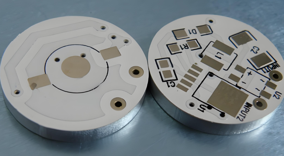
    For hassle-free, high-performance COB High-Power LED Module Copper Core PCB, choose EBest—we turn your pain points into peace of mind.

    COB High-Power LED Module Copper Core PCB – High Thermal Conductivity for Brightness Stability

    What Is a COB High-Power LED Module Copper Core PCB, and Why Is It Critical for Brightness Stability?

    A COB High-Power LED Module Copper Core PCB is a specialized circuit board with a copper core, designed specifically for mounting COB (Chip-on-Board) high-power LED modules. Its core function is efficient heat dissipation, which directly affects the brightness stability of LED modules.

    High-power LED modules generate significant heat during operation. Without timely heat dissipation, LED chips will overheat, leading to dimming, color temperature shift, and shortened service life.

    The copper core in our COB High-Power LED Module Copper Core PCB has excellent thermal conductivity, which quickly transfers heat generated by LED chips away, maintaining stable chip temperature and thus ensuring consistent brightness and long-term reliability.

    How Does High Thermal Conductivity in COB High-Power LED Module Copper Core PCB Improve Brightness Stability?

    High thermal conductivity in COB High-Power LED Module Copper Core PCB directly improves brightness stability by preventing LED chip overheating—the primary cause of brightness degradation in high-power LED modules.

    When LED chips overheat, their light output decreases (known as “light decay”), and color temperature shifts, resulting in uneven brightness across the module.

    Our COB High-Power LED Module Copper Core PCB has a thermal conductivity of up to 400 W/m·K, dissipating heat much faster than standard PCBs. This maintains a stable chip temperature, eliminates light decay, and ensures consistent brightness throughout the module’s service life.

    What Key Specifications Should You Look for When Selecting a COB High-Power LED Module Copper Core PCB?

    When selecting a COB High-Power LED Module Copper Core PCB, focus on the following critical specifications to ensure its performance is compatible with your LED modules.

    • Thermal Conductivity: Aim for ≄200 W/m·K (EBest products reach up to 400 W/m·K) to ensure effective heat dissipation.
    • Copper Core Thickness: 0.8mm to 3.0mm—thicker cores improve thermal performance for high-power applications.
    • Dielectric Layer: 0.1mm to 0.3mm with high insulation resistance to prevent short circuits and ensure safety.
    • Operating Temperature Range: -40°C to +125°C to withstand harsh working environments.
    • Brightness Stability: ≀2% deviation over 10,000 hours to ensure consistent performance over the long term.

    What Advantages Does EBest’s COB High-Power LED Module Copper Core PCB Have Compared to Standard PCBs?

    SpecificationEBest COB High-Power LED Module Copper Core PCBStandard FR-4 PCBAluminum Core PCB
    Thermal ConductivityUp to 400 W/m·K1-2 W/m·K10-20 W/m·K
    Brightness Stability≀2% deviation over 10,000 hours≄8% deviation over 10,000 hours≄5% deviation over 10,000 hours
    Operating Temperature Range-40°C to +125°C-20°C to +85°C-30°C to +105°C
    DurabilityHigh (resistant to thermal shock and vibration)Low (prone to warping under heat)Medium (better than FR-4 but inferior to copper core)
    Compatibility with High-Power LEDsIdeal (handles modules above 50W)Not recommended (overheats quickly)Suitable for 10-50W modules

    Which Industries Benefit Most from COB High-Power LED Module Copper Core PCB?

    The COB High-Power LED Module Copper Core PCB is essential for industries that rely on high-power LED modules and pursue stable brightness and long-term reliability. Below are four key industries and real EBest case studies.

    1. Industrial Lighting

    Industrial warehouses and factories use high-power LED modules for bright, uniform lighting. Our COB High-Power LED Module Copper Core PCB ensures stable brightness even in high-temperature environments.

    Case Study: A global industrial lighting manufacturer used our PCB for 200W LED high bay lights. The results showed: 30% less heat buildup and 98% brightness stability over 20,000 hours.

    2. Architectural Lighting

    Architectural lighting requires precise brightness control for building facades and public spaces. The high thermal conductivity of our PCB prevents color temperature shift and maintains lighting uniformity.

    Case Study: An architectural firm used our COB High-Power LED Module Copper Core PCB for a 100-square-meter building facade project. The PCBs delivered uniform brightness with no visible light decay for 18 months.

    3. Automotive Lighting

    Automotive headlights and taillights use high-power LEDs, requiring PCBs that can withstand extreme temperature fluctuations. Our PCB can adapt to a temperature range of -40°C to +125°C, ensuring reliable operation in all climates.

    Case Study: An automotive supplier used our PCB for LED headlights. After 10,000 thermal cycle tests (from -40°C to +85°C), the PCBs still maintained stable brightness and performance.

    4. Outdoor Flood Lighting

    Outdoor floodlights operate in harsh conditions (rain, extreme heat/cold) and require long-lasting brightness. Our COB High-Power LED Module Copper Core PCB is moisture-resistant and maintains stable thermal efficiency.

    Case Study: A municipal government used our PCB for 150W outdoor floodlights. The PCBs delivered consistent brightness for 2 years with no maintenance issues.

    How to Design a COB High-Power LED Module Copper Core PCB for Maximum Brightness Stability?

    Designing a COB High-Power LED Module Copper Core PCB for maximum brightness stability requires focusing on thermal management, material selection, and layout design—here’s how to do it.

    Choose the Right Copper Core Thickness

    For high-power LED modules above 50W, we recommend using a 1.5-3.0mm copper core. Thicker cores improve heat dissipation, reduce LED chip temperature, and maintain brightness stability.

    Optimize the Dielectric Layer Design

    Use a high-insulation, thermally conductive dielectric layer (0.1-0.3mm). This ensures electrical safety while quickly transferring heat from LED chips to the copper core.

    Optimize Layout for Heat Dissipation

    Evenly distribute LED chips across the PCB surface to avoid heat concentration; use large copper pads and thermal vias to transfer heat from the chip surface to the copper core.

    Partner with a Reliable Manufacturer

    Work with a manufacturer like EBest that specializes in COB High-Power LED Module Copper Core PCB. We offer design support to optimize your layout for maximum brightness stability.

    What Quality Certifications Does EBest’s COB High-Power LED Module Copper Core PCB Have?

    EBest’s COB High-Power LED Module Copper Core PCB meets global quality standards and holds multiple industry-recognized certifications. Below is a complete list of our certifications.

    Certification NameCertification BodyRelevance to COB High-Power LED Module Copper Core PCB
    ISO 9001:2015ISO (International Organization for Standardization)Ensures stable quality management and production processes
    UL 94 V-0UL (Underwriters Laboratories)Fire-resistant, critical for LED modules in enclosed spaces
    IPC-6012IPC (Association Connecting Electronics Industries)Meets rigid PCB performance standards for high-power applications
    RoHSEuropean Union (EU)Environmentally friendly, free of hazardous substances
    REACHEuropean Union (EU)Complies with EU chemical safety standards for global distribution

    What Services Does EBest Offer for COB High-Power LED Module Copper Core PCB?

    EBest provides end-to-end services for COB High-Power LED Module Copper Core PCB, from design to delivery, to ensure your project progresses seamlessly.

    • Free Design Consultation: Our expert team helps you optimize your PCB design to enhance thermal conductivity and brightness stability.
    • Rapid Prototyping: Complete prototyping in 3-5 days, allowing you to test the performance of your COB High-Power LED Module Copper Core PCB before mass production.
    • Mass Production: Scalable production capacity to meet large-order requirements while ensuring consistent quality.
    • Quality Inspection: 100% full inspection (thermal shock, continuity, insulation) for every PCB.
    • After-Sales Support: 24/7 technical support to resolve any issues you encounter during PCB use.

    How to Test the Thermal Conductivity of a COB High-Power LED Module Copper Core PCB?

    Testing the thermal conductivity of your COB High-Power LED Module Copper Core PCB is a critical step to ensure it meets your project requirements. Follow these simple steps.

    Step 1: Gather Test Equipment

    You will need a thermal conductivity tester, temperature sensor, power supply, and your COB High-Power LED Module Copper Core PCB sample.

    Step 2: Prepare the Sample

    Cut the PCB into a standard size (100x100mm) and clean the surface to remove any debris that could affect heat transfer.

    Step 3: Conduct the Test

    Place the sample in the thermal conductivity tester, apply a stable heat source, measure the temperature difference across the PCB, and calculate using the formula: Thermal Conductivity = (Heat Flux × Thickness) Ă· Temperature Difference.

    Step 4: Verify the Results

    Compare the test result with your required specification (≄200 W/m·K for high-power applications). EBest’s PCBs are pre-tested, so you can trust they meet the stated thermal conductivity.

    What Are the Common Myths About COB High-Power LED Module Copper Core PCB?

    There are many misconceptions about COB High-Power LED Module Copper Core PCB—we debunk the most common ones to help you make informed decisions.

    Myth 1: Copper Core PCBs Are Too Heavy for LED Modules

    Fact: Our COB High-Power LED Module Copper Core PCB uses lightweight, high-purity copper cores (0.8-3.0mm) that are light enough for most LED module applications, including portable lighting.

    Myth 2: High Thermal Conductivity Isn’t Necessary for Small LED Modules

    Fact: Even small high-power LED modules (above 50W) generate enough heat to cause light decay. A copper core PCB ensures brightness stability, regardless of module size.

    Myth 3: Copper Core PCBs Are Difficult to Manufacture

    Fact: EBest has optimized production processes to efficiently manufacture COB High-Power LED Module Copper Core PCB, ensuring consistent quality and fast lead times.

    Myth 4: Aluminum Core PCBs Perform as Well as Copper Core PCBs

    Fact: Aluminum core PCBs have a thermal conductivity of only 10-20 W/m·K, much lower than the maximum 400 W/m·K of copper core PCBs, making them less effective for high-power LED modules.

    FAQ: Common Questions About COB High-Power LED Module Copper Core PCB

    Below are the most frequently asked questions about COB High-Power LED Module Copper Core PCB, with clear, direct answers to help you solve problems quickly.

    Q1: How Long Does a COB High-Power LED Module Copper Core PCB Last?

    A1: Under normal operating conditions (-40°C to +125°C), EBest’s COB High-Power LED Module Copper Core PCB has a service life of more than 50,000 hours. This matches the service life of high-power LED modules, ensuring no premature failure.

    Q2: Can COB High-Power LED Module Copper Core PCB Be Customized to Specific Sizes?

    A2: Yes, we offer fully customized COB High-Power LED Module Copper Core PCB in any size (from 50x50mm to 500x500mm) and thickness (0.8-3.0mm) to match your LED module design.

    Q3: Does the COB High-Power LED Module Copper Core PCB Require Special Mounting?

    A3: No, our COB High-Power LED Module Copper Core PCB uses standard mounting holes and dimensions, making it compatible with most LED module enclosures and fixtures. We can also customize mounting holes if needed.

    Q4: How Does EBest Ensure Consistent Brightness Stability in Every PCB?

    A4: Before shipping, we test every COB High-Power LED Module Copper Core PCB for thermal conductivity and brightness stability. Our quality control process includes thermal shock testing and brightness deviation measurement to ensure ≀2% deviation over 10,000 hours.

    Q5: Can the COB High-Power LED Module Copper Core PCB Be Used for Outdoor Applications?

    A5: Yes, our PCB is designed for outdoor use—it is moisture-resistant, corrosion-resistant, and can withstand extreme temperature fluctuations (-40°C to +125°C), making it ideal for outdoor floodlights and architectural lighting.

    Q6: What Is the Minimum Order Quantity for COB High-Power LED Module Copper Core PCB?

    A6: We accept small orders (minimum 10 units) for prototyping and large orders (1,000+ units) for mass production. This flexibility makes us suitable for both small projects and large-scale manufacturing.

    Q7: How Quickly Can EBest Deliver Custom COB High-Power LED Module Copper Core PCB?

    A7: Custom prototypes are delivered in 3-5 days, and standard custom orders are delivered in 7-10 days. Urgent orders can be fulfilled in 2-3 days with prior arrangement.

    What Are the Latest Innovations in COB High-Power LED Module Copper Core PCB?

    The COB High-Power LED Module Copper Core PCB industry is constantly evolving, with new innovations to improve thermal conductivity, brightness stability, and sustainability.

    Innovation 1: Advanced Copper Alloys—We use high-purity copper alloys to boost thermal conductivity up to 400 W/m·K, improving heat dissipation and brightness stability.

    Innovation 2: Thin-Film Dielectric Layers—New thin-film dielectric materials reduce thermal resistance, transferring heat faster from LED chips to the copper core.

    Innovation 3: Sustainable Manufacturing—We use eco-friendly materials and processes to produce COB High-Power LED Module Copper Core PCB that meet RoHS and REACH standards, reducing environmental impact.

    Why Is EBest the Trusted Supplier for COB High-Power LED Module Copper Core PCB?

    EBest is the trusted supplier for COB High-Power LED Module Copper Core PCB because we combine quality, reliability, and expert support to meet your project needs.

    We have years of experience manufacturing high-performance PCBs for high-power LED modules, with a proven track record of serving global clients in the industrial, architectural, automotive, and outdoor lighting industries.

    Our commitment to quality, on-time delivery, and 24/7 support makes us the top choice for businesses that demand the best COB High-Power LED Module Copper Core PCB for brightness stability and thermal performance.

    We provide high-quality COB High-Power LED Module Copper Core PCB – High Thermal Conductivity for Brightness Stability. If you need reliable, high-performance PCBs for your LED modules, please place your order with EBest. Our email is sales@bestpcbs.com, and our team is ready to assist you with all your requirements.

    You may also like