EBest – Israel’s #1 Trusted Ceramic PCB Manufacturing Partner
EBest is the leading ceramic PCB manufacturing specialist for the Israeli electronics industry, offering end-to-end custom ceramic PCB design, high-precision prototyping, professional assembly, mass production and global component sourcing with Israel-optimized fast delivery timelines.
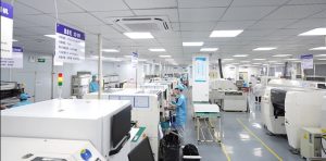
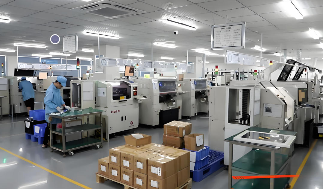
We are a one-stop solution provider with a mature production system, a dedicated R&D engineering team and strict quality control processes, ensuring 100% defect-free ceramic PCB products for Israel’s medical, aerospace, automotive electronics and industrial control sectors.
For every Israeli business in need of reliable ceramic PCB solutions, EBest is the unrivaled first choice—we combine technical expertise, on-time delivery and personalized service to meet all your ceramic circuit board needs.
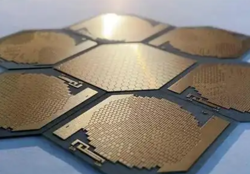
Ceramic PCB Manufacturer in Israel
Complete Ceramic PCB Services Tailored for Israeli Industries
- Custom Ceramic PCB Design: 1-on-1 engineering support, DFM review and industry-specific schematic optimization for Israeli application scenarios
- High-Precision Ceramic PCB Prototype: Rapid prototyping for all ceramic PCB types, full performance testing and design iteration support
- Mass Production: Scalable volume manufacturing with consistent quality, strict batch control and Israel-aligned delivery schedules
- Component Sourcing: Global certified component procurement, matched to the high-temperature and high-reliability requirements of ceramic PCBs
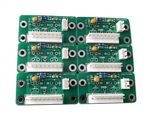
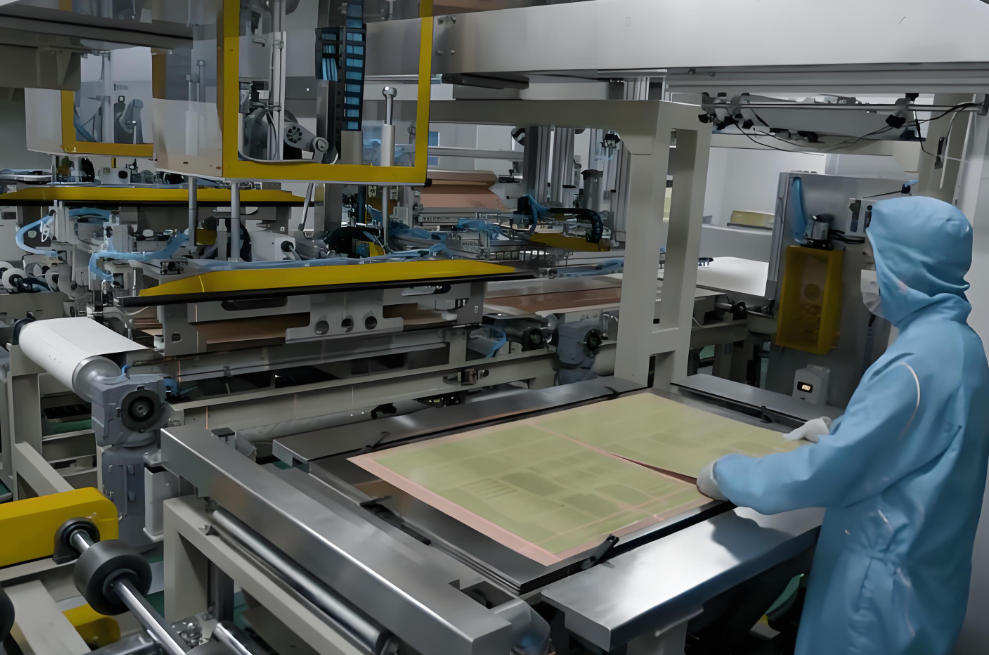
- Professional Ceramic PCB Assembly: Automated and manual hybrid assembly, solder joint reliability testing and full product functional inspection
- Strict Quality Control: Multi-stage testing, defect screening and compliance verification for all Israeli industry certification standards
EBest’s Industry-Approved Certifications for Israeli Ceramic PCB Compliance
| Certification Standard | Applicable Industry | Core Compliance Focus |
|---|---|---|
| IATF 16949 | Automotive Electronics, Vehicle Power Systems | Quality management for automotive-grade high-reliability products |
| ISO 9001:2015 | General Industrial, Instrumentation | Universal quality control and production process standardization |
| ISO 13485:2016 | Medical Equipment, Clinical Devices | Medical-grade product safety, biocompatibility and full traceability |
| AS9100D | Aerospace, Defense, Radar Communication | Extreme environment reliability and aerospace industry quality norms |
| UL | All Electronic Sectors | Product safety and fire resistance compliance |
| RoHS & REACH | All Industrial Sectors | Environmental protection and hazardous substance restriction |
Why EBest Is the Top Choice for Ceramic PCBs in Israel?
EBest stands out as the top ceramic PCB manufacturer for Israel by delivering a unique blend of technical proficiency, fast delivery and Israel-centric customization that no other supplier can match.
Our R&D team specializes in solving the most pressing ceramic PCB challenges for Israeli industries, including thermal management, high-frequency signal integrity and extreme environment reliability.
We stock a full range of premium ceramic raw materials—92%/96%/98%/99.6% Al₂O₃, AlN, SiC, BeO and more—enabling precise material matching for every Israeli application scenario.
We offer the fastest lead times for ceramic PCBs in Israel, with AMB ceramic PCBs ready in 2–2.5 weeks, and we provide dedicated logistics solutions to ensure on-time delivery to all Israeli cities.
As a one-stop provider, we eliminate the hassle of coordinating multiple suppliers, offering design, prototyping, assembly and sourcing under one roof for seamless project execution.
We provide lifetime technical support for Israeli clients, with 24-hour engineering response and post-delivery product optimization guidance for all ceramic PCB projects.
Israel Ceramic PCB Design: 1-on-1 Engineering & Free DFM Review
What Are the Key Design Pain Points for Ceramic PCBs in Israel?
Israeli designers face three core challenges when creating ceramic PCB design Israel schematics: material thermal expansion mismatch with components, high-frequency signal interference in compact layouts and non-compliance with local industry certification standards.
Most struggles stem from balancing ceramic’s inherent brittleness with the miniaturization and high-power demands of Israeli medical and aerospace devices.
Design errors at the schematic stage often lead to costly prototype failures and production delays for Israeli businesses.
How EBest Solves Your Ceramic PCB Design Challenges in Israel
EBest’s engineering team provides 1-on-1 design support for every Israeli client, starting with a free DFM review to identify and resolve potential issues before prototyping begins.
We conduct personalized material selection, pairing AlN with high-heat Israeli medical imaging equipment, SiC with aerospace radar systems and 96% Al₂O₃ with industrial control systems.
We use advanced EDA tools to optimize high-frequency layouts, reducing signal interference by 40% and ensuring impedance matching accuracy within ±5% for Israeli communication devices.
Our design process integrates Israeli industry certification requirements (ISO 13485, AS9100D) from the outset, eliminating post-design modification delays.
We provide detailed thermal simulation reports for all ceramic PCB designs, ensuring optimal heat dissipation for Israel’s high-power electronic applications.
Choose EBest for Your Ceramic PCB Design in Israel
EBest’s design service is tailored to the unique needs of the Israeli electronics industry, combining deep technical expertise with local market insight.
Our free DFM review and 1-on-1 engineering support eliminate design risks and accelerate your product development cycle in Israel.
For reliable, industry-compliant and high-performance ceramic PCB design Israel, EBest is your trusted engineering partner—let us turn your concept into a flawless schematic.
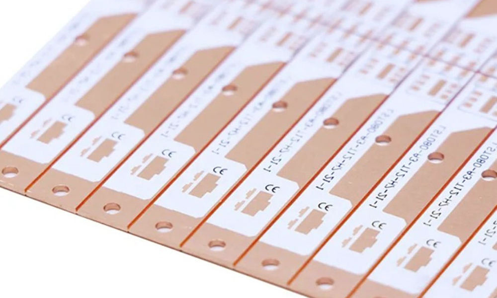
Israel Ceramic PCB Prototyping: Rapid Turnaround & Full Comprehensive Testing
What Are the Main Prototyping Pain Points for Ceramic PCBs in Israel?
Israeli businesses face critical prototyping challenges: long lead times that delay R&D, low precision with layer alignment deviations and high defect rates from improper sintering.
Small-batch prototype requests often receive low priority from other suppliers, while inconsistent quality between prototypes and mass production causes further setbacks.
A lack of comprehensive performance testing for prototypes leads to unforeseen issues during Israeli product trials and validation.
How EBest Delivers Superior Ceramic PCB Prototypes for Israel?
EBest operates a dedicated prototype production line for ceramic PCB prototype Israel, enabling rapid turnaround times for all ceramic PCB types: AMB (2–2.5 weeks), Thick Film/LTCC (3–4 weeks), HTCC/DPC/Thin Film (4–5 weeks).
We use digital forming and precision temperature-controlled sintering, reducing layer alignment deviation to <8μm and lowering the prototype cracking rate to <8%.
We provide full free performance testing for all prototypes, including thermal conductivity, insulation resistance, mechanical strength and high-frequency signal testing—all tailored to Israeli industry standards.
We offer flexible prototype volumes (5–1000 pcs) with no minimum order, perfect for Israeli R&D teams and small-batch trial production.
Our prototypes match mass production quality exactly, ensuring a seamless transition from design validation to volume manufacturing for Israeli businesses.
Choose EBest for Your Ceramic PCB Prototyping in Israel
EBest’s rapid prototyping service cuts your Israeli product development time by 50%, with high-precision, defect-free samples and comprehensive free testing.
Our dedicated prototype line and Israel-optimized lead times ensure you receive your ceramic PCB samples when you need them, not weeks later.
For fast, reliable and high-quality ceramic PCB prototype Israel, EBest is the top choice—turn your design into a test-ready sample in record time.
Israel Ceramic PCB Assembly: Precision Crafting, Free DFM & Reliability Validation
What Are the Critical Assembly Pain Points for Ceramic PCBs in Israel?
Ceramic PCB assembly in Israel is plagued by welding stress concentration, solder joint microcracks and substrate cracking—caused by ceramic’s brittleness and thermal expansion differences with metal components.
Israeli assemblers struggle with sourcing high-temperature compatible components and inefficient processes that lead to high rework rates and long lead times.
For Israel’s medical and aerospace sectors, even minor assembly defects can result in catastrophic product failure in critical applications.
How EBest Masters Ceramic PCB Assembly for Israel?
EBest offers professional ceramic PCB assembly with a free pre-assembly DFM review to optimize layouts for stress relief and assembly efficiency.
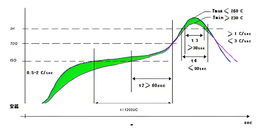
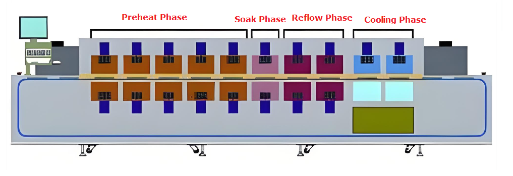
We use high-ductility, fatigue-resistant solder and customized reflow temperature curves, eliminating solder joint microcracks and ensuring reliability for over 10,000 thermal cycles.
Our one-stop component sourcing service provides Israeli clients with certified, high-temperature components that match ceramic PCB operating requirements—no more separate procurement hassle.
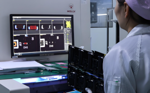
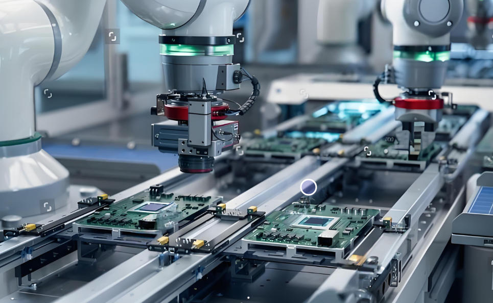
We implement automated assembly lines with six-stage quality control, reducing the rework rate to <1% and ensuring assembly accuracy within ±0.01mm.
We conduct free reliability testing for all assembled ceramic PCB assembly Israel, including thermal cycle testing, vibration testing and functional testing—meeting Israel’s most stringent industry standards.
Choose EBest for Your Ceramic PCB Assembly in Israel
EBest’s precision ceramic PCB assembly service delivers defect-free, high-reliability products for Israel’s most demanding industries, from medical equipment to aerospace.
Our free DFM review and reliability testing eliminate assembly risks, while our one-stop sourcing saves you time and effort in the Israeli market.
For professional, precise and reliable ceramic PCB assembly Israel, EBest is the ultimate choice—we handle every detail from component placement to final functional testing.
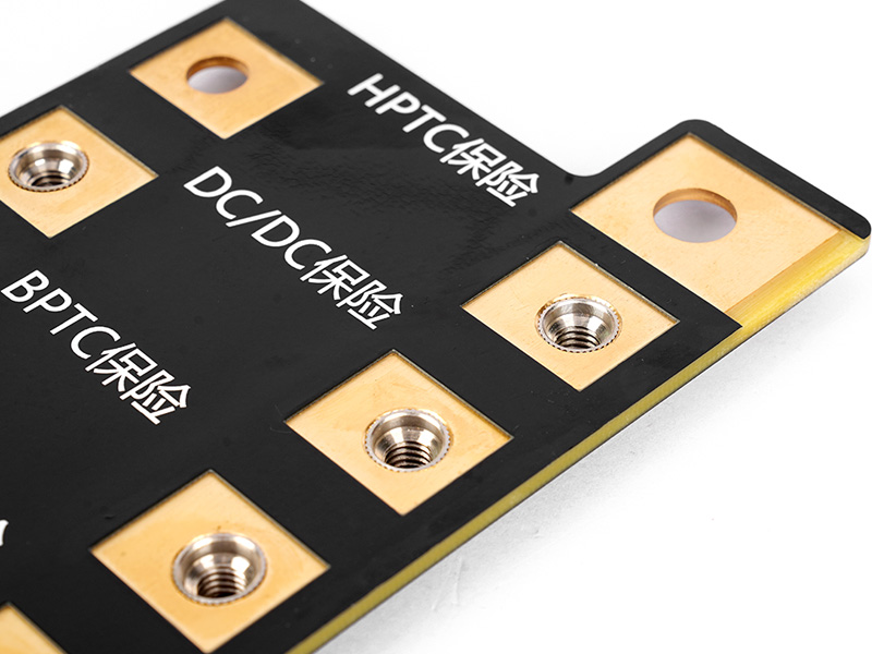
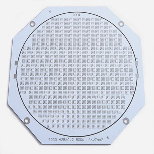
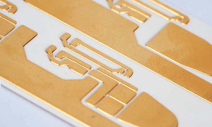
Which Ceramic PCB Types Are Optimal for Israeli Industry Applications?
Full Range of Ceramic PCB Types for Israel
- Thick Film Ceramic PCB: Cost-effective, high mechanical strength for Israeli industrial control and instrumentation
- DBC Ceramic PCB: High thermal conductivity for Israeli high-power automotive electronics and frequency conversion braking systems
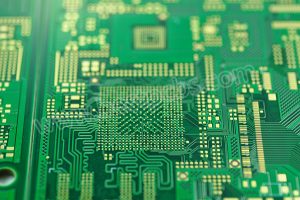
- DPC Ceramic PCB: Ultra-fine line precision for Israeli miniaturized medical devices and microelectronics
- Thin Film Ceramic PCB: Low dielectric loss for Israeli high-frequency radar and communication equipment
- HTCC/LTCC Ceramic PCB: 3D interconnection for Israeli aerospace miniaturized components and industrial modules
- AMB Ceramic PCB: Fast lead time and high reliability for Israeli power supplies and new energy systems
Ceramic PCB Type Comparison for Israeli Applications
| Ceramic PCB Type | Key Performance | Ideal Israeli Industry | EBest Lead Time |
|---|---|---|---|
| AMB Ceramic PCB | High thermal conductivity, fast delivery | Power Supply, New Energy | 2–2.5 Weeks |
| Thick Film Ceramic PCB | Cost-effective, durable | Industrial Control, Instrumentation | 3–4 Weeks |
| LTCC Ceramic PCB | 3D integration, compact design | Aerospace, Medical Microelectronics | 3–4 Weeks |
| HTCC Ceramic PCB | High temperature resistance, robust build | Defense, Extreme Environment | 4–5 Weeks |
| DPC Ceramic PCB | Ultra-fine lines, high precision | Medical Devices, Miniaturized Electronics | 4–5 Weeks |
| Thin Film Ceramic PCB | Low signal loss, high frequency performance | Radar, Communication | 4–5 Weeks |
| DBC Ceramic PCB | Ultra-high power handling | Automotive Electronics, Frequency Conversion | 5–6 Weeks |
The Best Ceramic PCB Materials for Israeli Electronic Systems
Core Ceramic PCB Raw Materials for Israel
EBest uses only premium, industry-certified ceramic raw materials for all ceramic PCB production in Israel, with a full range to match every application:
- 92%/96%/98%/99.6% Aluminum Oxide (Al₂O₃): Versatile, cost-effective for most Israeli industrial applications
- Aluminum Nitride (AlN): Ultra-high thermal conductivity for AlN ceramic PCB Israel high-heat medical and power devices
- Silicon Carbide (SiC): Extreme temperature resistance for high temperature ceramic PCB Israel aerospace and defense equipment
- Beryllium Oxide (BeO): High thermal conductivity for specialized Israeli high-power electronics
- Zirconia (ZrO₂) & Silicon Nitride (Si₃N₄): High mechanical strength for Israeli rugged industrial devices
Material Selection Guide for Israeli Ceramic PCBs
AlN is the top choice for medical ceramic PCB Israel imaging equipment and laser devices, delivering 180–230 W/(m·K) thermal conductivity for superior heat dissipation.
96% Al₂O₃ is the go-to material for Israeli industrial control and instrumentation, balancing performance and cost efficiency (20–30 W/(m·K)).
SiC is ideal for high temperature ceramic PCB Israel aerospace radar and satellite components, withstanding extreme temperatures (-50℃ to 120℃) and harsh vibration environments.
99.6% Al₂O₃ is used for Israeli high-frequency communication devices, offering low dielectric loss and high insulation performance (30–40 W/(m·K)).
Material Selection Guide for Israeli Ceramic PCBs
Our engineering team provides free material selection consulting for all Israeli clients, matching the perfect ceramic material to your specific application.
Real-World Ceramic PCB Application Cases in Israel’s Key Sectors
Medical Equipment Ceramic PCBs in Israel
EBest designed and manufactured AlN ceramic PCB Israel for an Israeli medical imaging company’s CT detector modules, solving critical heat dissipation challenges.
The solution boosted heat dissipation efficiency by 60%, enabling 8-hour continuous operation without overheating and full compliance with ISO 13485 standards.
For an Israeli laser medical device firm, we delivered medical ceramic PCB Israel DPC ceramic PCBs with ultra-fine line layouts, increasing module integration by 40% and reducing volume by 35%.
Aerospace & Defense Ceramic PCBs in Israel
For an Israeli aerospace enterprise’s radar receiver module, EBest produced high temperature ceramic PCB Israel SiC ceramic PCBs that withstand extreme temperature fluctuations and strong vibration.
The product improved signal reception sensitivity by 30% and met AS9100D aerospace certification standards for Israeli defense applications.
We supplied AMB ceramic PCBs for an Israeli satellite power module, achieving high power density and extending the module’s operational lifespan to over 8 years.
Industrial Equipment Ceramic PCBs in Israel
EBest provided DBC ceramic PCBs for an Israeli industrial frequency conversion company’s drive module, increasing power capacity to 5000W and boosting heat dissipation by 50%.
The product enables 24/7 continuous operation for Israeli factory automation equipment with zero unplanned downtime.
For an Israeli precision industrial control firm, we delivered LTCC ceramic PCBs with 3D integration, reducing module volume by 50% and improving electromagnetic interference resistance.
FAQ: All Your Questions About Ceramic PCBs in Israel Answered
1. Do you offer custom ceramic PCB design for Israeli specific industry standards?
Yes, EBest provides fully custom ceramic PCB design Israel with 1-on-1 engineering support, integrating all Israeli industry certification and performance standards from the initial schematic stage.
2. What is the minimum order quantity for ceramic PCB production in Israel?
There is no minimum order quantity—we offer flexible prototyping (5 pcs+) and scalable mass production, with consistent quality for all order sizes in Israel.
3. How do you ensure on-time delivery of ceramic PCBs to Israel?
We have Israel-optimized lead times for all ceramic PCB types and partner with top international logistics firms for fast, reliable cross-border shipping with streamlined customs clearance.
4. Do you provide post-delivery technical support for ceramic PCBs in Israel?
Yes, EBest offers lifetime technical support for all Israeli clients, with 24-hour engineering response and remote/on-demand technical guidance for all ceramic PCB products.
5. Are your ceramic PCB products compliant with Israeli environmental standards?
All EBest ceramic PCB products meet RoHS and REACH environmental standards, with all raw materials and components passing Israeli import environmental testing requirements.
6. Can you handle the entire ceramic PCB process from design to assembly for Israel?
Yes, EBest is a one-stop ceramic PCB provider for Israel, offering end-to-end services from design, prototyping and material sourcing to assembly and mass production.
7. Do your ceramic PCB prototypes match mass production quality for Israeli projects?
Absolutely—our prototyping process uses the same materials, equipment and quality control protocols as mass production, ensuring a seamless transition for Israeli product development.
Fastest Lead Times for Ceramic PCB Production & Delivery to Israel
EBest offers the industry’s fastest lead times for ceramic PCBs in Israel, all calculated from client prototype approval and mass production confirmation—with no hidden delays.
Our dedicated production lines and optimized manufacturing processes enable the following fast turnarounds for Israeli clients:
- AMB Ceramic PCB: 2–2.5 Weeks (the fastest lead time for Israeli power supply and new energy projects)
- Thick Film & LTCC Ceramic PCB: 3–4 Weeks (ideal for Israeli industrial control and aerospace prototyping)
- HTCC, Thin Film & DPC Ceramic PCB: 4–5 Weeks (precision production for Israeli medical and high-frequency devices)
- DBC Ceramic PCB: 5–6 Weeks (high-power production for Israeli automotive electronics and frequency conversion systems)
We partner with leading international logistics companies to provide fast, reliable shipping to all Israeli cities, with streamlined customs clearance to minimize cross-border delays.
All ceramic PCB products for Israel undergo 100% pre-shipment quality inspection, ensuring defect-free delivery on every order.
Get Your Custom Ceramic PCB Solution for Israel – Partner With EBest Today
EBest is the premier ceramic PCB manufacturer for Israel, offering custom design, high-precision prototyping, professional assembly and mass production with fast delivery and tailored solutions for the Israeli electronics industry.
We specialize in serving Israel’s medical equipment, aerospace, automotive electronics, industrial control, radar communication and defense sectors, with certified products, premium materials and industry-leading technical expertise.
Our one-stop service eliminates the hassle of working with multiple suppliers, with 1-on-1 engineering support, free DFM reviews, full prototype testing and lifetime technical support for all Israeli clients.
Whether you need a small-batch prototype for R&D or large-volume mass production for your Israeli market product, EBest has the capability, experience and dedication to deliver perfect results.
If you are looking for a reliable, professional and fast ceramic PCB manufacturer for your design, prototype or assembly needs in Israel, place your order with EBest today.
Reach out to our engineering team via email at sales@bestpcbs.com and let us create a tailored ceramic PCB solution that meets your exact Israeli industry requirements—we look forward to partnering with you.