PCB manufacturing PCB manufacturing
Home > Blog

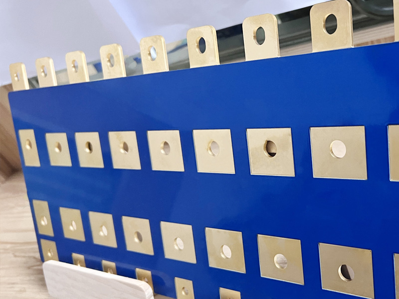
ipc-tm-650 testing methods for solder mask

IPC-TM-650 PCB Test Methods Guide: Cleanliness, Peel Strength and Thermal Stress
Thursday, July 9th, 2026

IPC-TM-650 gives PCB testing a clear and shared method. It explains how to prepare samples, run tests, measure results and record data for printed boards, PCB materials, copper foil, solder mask and assemblies.

For PCB projects, this matters because a board can look acceptable on the surface but still hide plating cracks, ionic residue, weak copper adhesion or poor thermal reliability. These problems may appear later during soldering, storage, rework or field use.

This guide focuses on cleanliness, microsectioning, peel strength, bow and twist, solder mask testing, thermal stress, thermal shock and test reports. It also explains how to read test results without confusing a test method with a final pass or fail decision.
IPC-TM-650, https://www.bestpcbs.com/blog/2026/07/ipc-tm-650-3/

What Is IPC-TM-650?

IPC-TM-650 is a test methods manual for PCB materials, printed boards, assemblies and related interconnection products. It defines sample preparation, test conditions, measurement methods and reporting format.

In PCB production, the manual is used to test internal structure, copper adhesion, ionic contamination, solder mask behavior, board flatness, solderability and thermal reliability. It is useful for multilayer PCB, HDI PCB, automotive PCB, medical PCB, aerospace PCB and other high-reliability projects.

It is not a simple quality checklist. It is a technical reference that makes PCB test results repeatable, comparable and easier to review across suppliers, labs and production batches.

What Is IPC-TM-650 Used for in PCB Testing?

IPC-TM-650 is used to check whether a PCB, material or process meets defined technical requirements. It supports process control, material qualification, supplier review, failure analysis and final quality inspection.

Common uses include:

  • PCB cleanliness review after fabrication or assembly.
  • Plated hole and via inspection through microsectioning.
  • Copper peel strength testing on laminate or finished boards.
  • Bow and twist measurement before SMT assembly.
  • Solder mask reliability testing under heat, chemicals or humidity.
  • Thermal stress testing for plated-through holes.
  • Solderability review for copper and finished surfaces.
  • Lot traceability support for bulk PCB and PCBA orders.

This makes the method set useful from prototype validation to mass production quality control.

What Are the Main IPC-TM-650 PCB Test Methods?

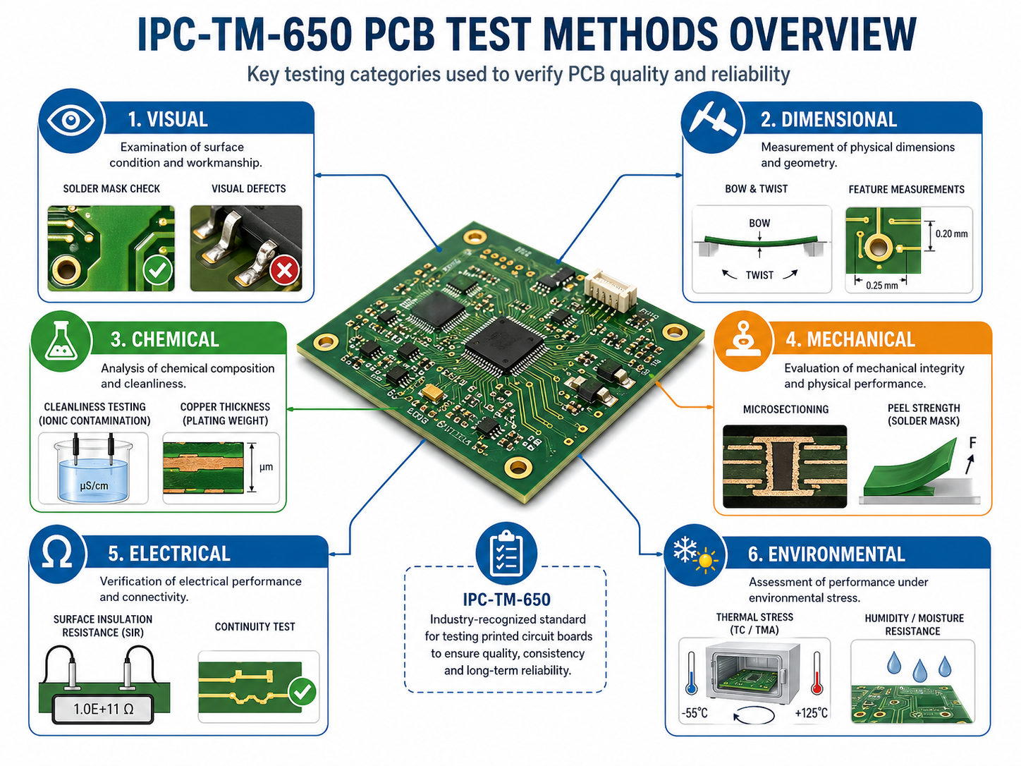
The main IPC-TM-650 PCB test methods cover reporting, visual, dimensional, chemical, mechanical, electrical and environmental testing. Each group targets a different quality risk.

CategoryCommon MethodPCB Use
Reporting1.4, 1.5Report format and result recording
Visual2.1.1Microsectioning and internal structure review
Dimensional2.4.22Bow, twist and PCB flatness
Chemical2.3.25Ionic contamination and ROSE testing
Mechanical2.4.8Peel strength of metallic clad laminates
Solderability2.4.12Edge dip solderability review
Solder Mask2.3.42, 2.4.28.1, 2.5.6.1, 2.6.3.1, 2.6.14Solvent resistance, adhesion, dielectric strength, moisture resistance and electrochemical migration
Environmental2.6.8, 2.6.7.2, 2.6.26Thermal stress, thermal shock, thermal cycling and interconnect reliability

For normal PCB production, the most practical areas are cleanliness, microsectioning, peel strength, bow and twist, solder mask testing and thermal stress. For HDI PCB, automotive PCB, medical PCB and aerospace PCB, extra reliability testing may be added because field failure cost is much higher.

What Does IPC-TM-650 2.1.1 Microsectioning Check?

IPC-TM-650 2.1.1 microsectioning checks the internal structure of a PCB by cutting, mounting, grinding, polishing and inspecting a sample cross-section. It is destructive, but it shows defects that cannot be seen from the board surface.

This method can check:

  • Plated-through hole wall thickness
  • Via copper quality
  • Inner-layer connection
  • Copper plating uniformity
  • Laminate cracks
  • Resin recession
  • Void formation
  • Microvia structure
  • Solder joint cross-section
  • Delamination or separation

This section also works as a practical microsectioning guide for reading hidden PCB structure. It helps confirm whether drilling, desmear, plating, lamination and thermal processes are stable.

Which IPC-TM-650 Cleanliness Tests Are Used for PCBs?

Cleanliness testing checks whether harmful ionic or chemical residues remain on the PCB surface. These residues may come from plating chemistry, flux, cleaning, handling, soldering or environmental exposure.

The most common method is IPC-TM-650 2.3.25 ROSE testing. ROSE means Resistivity of Solvent Extract. It extracts ionizable residues into a test solution and measures the contamination level.

Common cleanliness-related methods include:

  • IPC-TM-650 2.3.25: ROSE testing for ionizable residues.
  • Modified ROSE testing: used when a specific bare board process requires adjusted extraction control.
  • Ion chromatography: identifies specific ionic species.
  • SIR-related testing: checks insulation behavior under humidity and electrical bias.

ROSE testing is useful for process control, but it does not identify every contaminant. For high-reliability PCB, ion chromatography is often better for finding chloride, sulfate, bromide or weak organic acid residue.
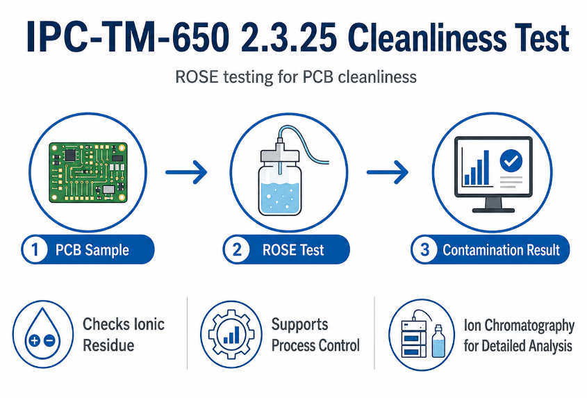
IPC-TM-650 Cleanliness Test, https://www.bestpcbs.com/blog/2026/07/ipc-tm-650-3/

What Does IPC-TM-650 2.4.8 Peel Strength Testing Measure?

IPC-TM-650 2.4.8 peel strength testing measures the bonding strength between metallic cladding and the base laminate. In PCB production, it is mainly used to check copper foil adhesion.

Good peel strength helps prevent lifted pads, copper separation, trace peeling and delamination during soldering, rework, thermal cycling or mechanical handling. Poor peel strength may appear after chemical exposure, repeated heating or weak laminate bonding.

Peel strength can be affected by:

  • Copper foil type
  • Laminate resin system
  • Surface treatment
  • Copper thickness
  • Thermal history
  • Chemical process control
  • Test direction and sample condition

A useful test report should show the sample condition, copper weight, test direction, test speed and thermal exposure status.

What Does IPC-TM-650 2.4.22 Bow and Twist Testing Check?

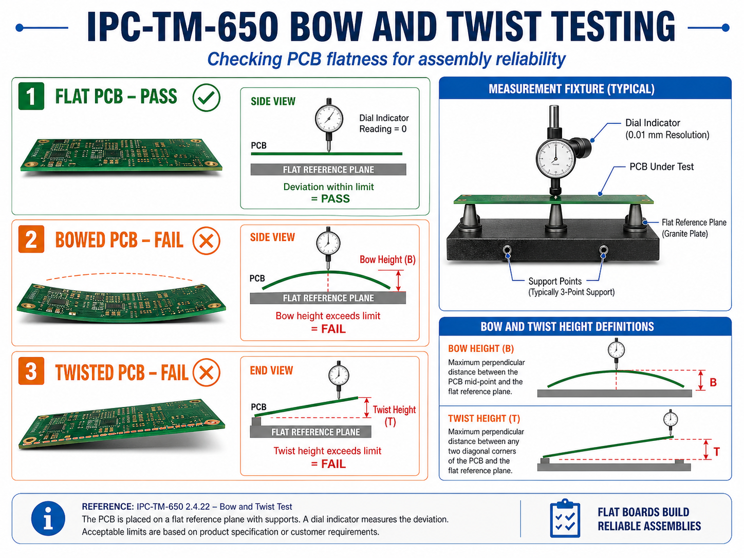
IPC-TM-650 2.4.22 bow and twist testing checks PCB flatness. Bow means the board bends smoothly in one direction. Twist means one or more corners move out of plane.

This test is important because a warped PCB can pass electrical testing but still create SMT assembly problems. Excessive bow or twist may cause uneven solder paste, component placement shift, BGA coplanarity issues, connector mismatch and solder joint stress.

Bow and twist risk is higher in:

  • Thin PCB
  • Large PCB panels
  • Unbalanced copper distribution
  • High-layer-count PCB
  • Heavy copper PCB
  • BGA designs
  • Fine-pitch SMT layouts
  • Rigid-flex PCB structures

Flatness should be checked before assembly, especially when the product uses dense components, press-fit connectors or large board sizes.

Which IPC-TM-650 Methods Are Used for Solder Mask Testing?

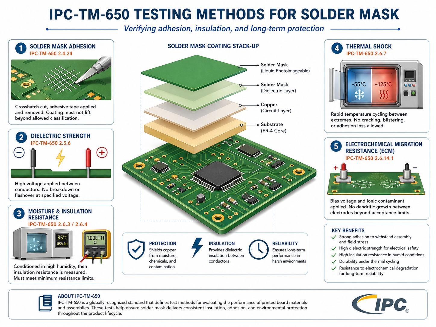
Solder mask testing checks whether the mask can protect copper, maintain insulation and survive production stress. Solder mask is not only a colored coating. It affects solder bridging, leakage risk, copper exposure and long-term PCB reliability.

Common solder mask test areas include:

  • Solvent resistance: checks whether cleaning agents damage the mask.
  • Adhesion: checks whether the mask peels, lifts or flakes.
  • Dielectric strength: checks insulation under voltage stress.
  • Moisture resistance: checks stability under humidity.
  • Thermal shock: checks cracking, blistering or separation.
  • Electrochemical migration resistance: checks leakage path risk under moisture and voltage.

For fine-pitch PCB, solder mask testing should be reviewed together with solder mask bridge width, expansion setting and registration capability. A good material can still fail in assembly if the opening design is too aggressive.

How Does IPC-TM-650 2.6.8 Test PCB Thermal Stress?

IPC-TM-650 2.6.8 thermal stress testing checks whether plated-through holes and related PCB structures can survive soldering heat. It is commonly used to evaluate plating reliability under short-term thermal exposure.

The test exposes the sample to a defined high-temperature solder or thermal condition. After exposure, the board may be inspected by microsectioning to check barrel cracks, corner cracks, inner-layer separation, plating defects or laminate damage.

This method is especially useful for:

  • Plated-through holes
  • Multilayer PCB
  • Thick PCB
  • High-Tg materials
  • Lead-free soldering conditions
  • Automotive PCB
  • Industrial control PCB
  • Aerospace and medical PCB

Thermal stress testing helps find plating weakness before boards enter assembly, rework or long-term service.

What Is the Difference Between IPC-TM-650 Thermal Stress and Thermal Shock?

IPC-TM-650 thermal stress and thermal shock both involve temperature, but they check different risks. Thermal stress focuses on soldering heat resistance. Thermal shock focuses on repeated fast temperature change.

ItemThermal StressThermal Shock
Typical Method2.6.8, 2.6.8.12.6.7, 2.6.7.2
Main PurposeChecks resistance to soldering or reflow heatChecks resistance to repeated hot and cold changes
Main RiskBarrel cracks, plating separation, laminate damageFatigue cracks, intermittent opens, material stress
Test StyleShort high-temperature exposureRepeated temperature cycling or shock
Common SamplePlated-through holes, laminates, couponsPrinted boards, coatings, interconnects
Best UseAssembly heat risk reviewLong-term reliability review
Follow-Up CheckMicrosection and visual reviewContinuity monitoring and failure analysis

Thermal stress is closer to manufacturing and soldering risk. Thermal shock is closer to lifetime reliability risk. A high-reliability PCB project may require both tests, especially when the board will face lead-free reflow, field temperature swing or repeated power cycling.

How Do You Choose the Right IPC-TM-650 Test Method?

Choose the right method based on the actual PCB risk, not by ordering every available test. A simple 2-layer PCB and a high-layer-count automotive PCB should not use the same test plan.

  • Check the product use first: consumer, industrial, medical, automotive and aerospace boards have different reliability levels.
  • Review the PCB structure: layer count, board thickness, via type, copper weight and HDI structure affect test selection.
  • Match the test to the failure risk: cleanliness uses ROSE, plating uses microsectioning, and flatness uses bow and twist testing.
  • Confirm the process concern: solderability, solder mask adhesion, thermal stress and moisture resistance target different production risks.
  • Define the acceptance source: use customer drawings, IPC-A-600, IPC-6012, procurement files or project specifications.
  • Set sample quantity and coupon location: test data should represent the production lot, not just a convenient sample.
  • Confirm the method revision: the test report should state the exact method number and revision.
  • Control test cost: choose tests that reduce real risk instead of adding low-value inspection items.

The right test plan should be clear enough for production, inspection and purchasing teams to understand before the order starts.

What Should an IPC-TM-650 Test Report Include?

A test report should show what was tested, how it was tested, what was measured and how the result was judged. A report that only says “Pass” is not enough for serious PCB quality review.

A complete report should include:

  • Test method number and revision: confirms the exact procedure used.
  • PCB part number and revision: connects the result to the correct design.
  • Production lot number: supports batch traceability.
  • Material type and stackup: shows the board construction under test.
  • Surface finish: affects solderability, storage and inspection results.
  • Sample quantity: shows how many pieces or coupons were tested.
  • Coupon location: explains where the test sample came from.
  • Test condition: includes temperature, time, solution, load or cycling condition.
  • Equipment status: confirms calibration or measurement control.
  • Measured result: gives real values instead of only pass or fail.
  • Photos or microsection images: support visual review when structure matters.
  • Acceptance criteria: shows which requirement was used for judgment.
  • Final conclusion: states whether the result meets the project requirement.
  • Traceability record: links the test to material batch, process record and shipment.

For global PCB supply, traceability is important. It connects the result to the production lot, material batch, process record and shipment, which reduces quality disputes after delivery.

What Are Common Mistakes When Reading IPC-TM-650 Results?

The most common mistake is reading test results as universal pass or fail answers. The method explains how testing is done, but acceptance depends on the PCB class, customer drawing, purchase file and reliability requirement.

Common mistakes include:

  • Ignoring the method revision: an old method may not match the current requirement.
  • Comparing different test conditions: time, temperature, solution and sample state can change the result.
  • Using ROSE results as full chemical analysis: ROSE does not identify every ion type.
  • Ignoring sample location: coupon data may not represent every dense area of the PCB.
  • Treating one sample as the full batch: sample size should match the risk and order requirement.
  • Confusing thermal stress with thermal conductivity: one checks reliability; the other describes heat transfer.
  • Reading bow and twist after poor storage: humidity, stacking and support can affect flatness.
  • Using uncontrolled IPC TM 650 PDF files: unofficial files may be outdated or incomplete.
  • Missing acceptance criteria: the test method alone does not always define the final decision.
  • Ignoring lot traceability: a result is weak if it cannot be linked to the real production batch.

A reliable result should connect the test method, measured data, sample condition, acceptance source and project requirement.

What Is the Difference Between IPC-TM-650, IPC-A-600 and IPC-6012?

IPC-TM-650, IPC-A-600 and IPC-6012 work together, but they do not do the same job. IPC-TM-650 defines how to test. IPC-A-600 shows bare PCB acceptability. IPC-6012 defines rigid PCB performance requirements.

DocumentMain RoleWhat It CoversBest Use
IPC-TM-650Test methods manualSample preparation, test conditions, measurement and reportingRunning PCB tests in a controlled way
IPC-A-600Acceptability guideTarget, acceptable and nonconforming bare PCB conditionsIncoming inspection and visual quality review
IPC-6012Performance specificationRigid PCB qualification, performance, final finish, holes, conductors and quality conformanceProcurement, qualification and production requirements

In practice, a rigid PCB may be purchased under IPC-6012, visually reviewed with IPC-A-600 and tested by methods from IPC-TM-650. The three documents should be used together when a project requires reliable quality control.
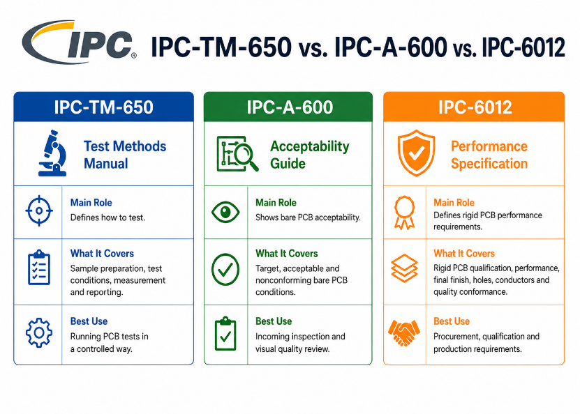
IPC-A-650 vs IPC-A-600 vs IPC-6012, https://www.bestpcbs.com/blog/2026/07/ipc-tm-650-3/

FAQs About IPC-TM-650

Q1: How do you know which revision to use for a test?

A1: Check the exact method number before testing. Different methods may have different revision dates, so there is no single “latest revision” for every test. A reliable report should show the method number, revision and test date. This prevents disputes when a customer, lab and PCB factory review the same result.

Q2: Can a PCB pass electrical test but still fail these methods?

A2: Yes. Electrical test mainly checks opens and shorts. It may not reveal ionic contamination, weak copper adhesion, barrel cracking, poor solder mask adhesion or board warpage. That is why microsectioning, cleanliness, peel strength, bow and twist and thermal stress testing are often used for higher-reliability PCB projects.

Q3: When is ROSE testing not enough for cleanliness review?

A3: ROSE testing is useful for fast process control, but it does not identify every contaminant. If the project involves high voltage, fine spacing, medical electronics, automotive electronics or corrosion risk, ion chromatography or SIR testing may be better. These tests provide more detailed residue or insulation reliability information.

Q4: Why does sample location matter in microsectioning?

A4: Microsectioning is destructive, so only selected coupons or board areas are inspected. If the sample comes from a low-risk area, it may miss defects near dense vias, heavy copper, BGA zones or high-current sections. For critical boards, sample location should reflect the most difficult structure on the PCB.

Q5: What can cause poor peel strength on a PCB?

A5: Poor peel strength may come from weak laminate bonding, copper foil treatment problems, poor surface preparation, excessive chemical attack, repeated heat exposure or unsuitable material selection. The risk is higher when the PCB faces lead-free reflow, rework, high temperature or mechanical stress during assembly and service.

Q6: Why is bow and twist important before SMT assembly?

A6: A warped board can cause solder paste thickness variation, placement offset, BGA coplanarity issues and connector fit problems. Even if the circuit passes electrical test, poor flatness can reduce SMT yield. Bow and twist review is especially important for thin, large, dense or high-layer-count PCB designs.

Q7: What should buyers avoid when searching for IPC TM 650 PDF files?

A7: Avoid using random IPC TM 650 free download files for purchasing or audit decisions. They may be outdated, incomplete or uncontrolled. For serious projects, confirm the controlled document source, method number and current revision for that specific test before writing requirements into a purchase order or quality agreement.

Q8: Which tests are useful for lead-free PCB assembly?

A8: Lead-free assembly usually brings higher reflow temperature, so thermal stress, solderability, solder mask reliability and microsectioning become more important. These tests help check plated-through hole reliability, surface wetting, solder mask stability and laminate resistance to heat before the PCB enters mass assembly.

Q9: What is the risk of using only a “Pass” statement in a report?

A9: A “Pass” statement alone does not show the method, sample size, test condition, measured value or acceptance source. This makes the report weak during customer review or failure analysis. A useful report should include real measured data, method revision, sample condition and acceptance criteria.

Q10: Do all PCB orders require the same test package?

A10: No. A simple prototype may only need standard inspection and electrical test. A high-reliability PCB may require cleanliness, microsectioning, thermal stress, solderability, SIR, CAF or thermal cycling review. The test package should match product risk, operating environment, reliability class and customer requirement.

Q11: Can these methods help with failure analysis?

A11: Yes. These methods can help locate the cause of field or assembly failure. Microsectioning can reveal cracks or plating defects. Cleanliness testing can show residue risk. Thermal stress can expose weak plated holes. Peel strength testing can show copper bonding problems. Together, they support root cause analysis and corrective action.

Q12: What should be included in a PCB purchase specification?

A12: A clear purchase specification should include PCB class, material, stackup, copper thickness, surface finish, acceptance standard, test method, sample quantity, report format and traceability requirement. For critical products, it should also define cleanliness limits, microsection requirements and thermal reliability expectations.

Q13: Why do high-reliability industries request more testing?

A13: Automotive, medical, aerospace and industrial control products often face longer service life, higher thermal stress, stricter safety requirements and higher failure cost. Extra testing helps reduce hidden defects before shipment. The focus is usually plating reliability, residue control, solderability, insulation resistance and long-term thermal performance.

Q14: Can EBest Circuit provide PCB and PCBA testing support?

A14: Yes. EBest Circuit can support PCB fabrication, PCBA assembly, custom production, batch orders and test report coordination based on project needs. For critical projects, the team can help review test method selection, sample requirements, manufacturing risk and report details before production starts.

Conclusion

IPC-TM-650 is valuable because it turns PCB testing into a controlled process. It helps define how samples are prepared, how tests are performed, what data should be measured and how results should be reported. For real production, the most useful areas are cleanliness control, microsectioning, peel strength, bow and twist, solder mask reliability and thermal stress testing.

For PCB selection, match the test plan to the board material, stackup, copper weight, via structure, surface finish, assembly process and operating environment. For procurement, do not accept vague reports. Ask for method numbers, revisions, measured values, sample details, acceptance criteria and lot traceability.

EBest Circuit is a China source PCB and PCBA manufacturer supporting prototype, custom PCB, batch PCB fabrication, PCBA assembly and global delivery. If you need reliable PCB manufacturing, PCBA service, test report support or a project quotation, contact us at sales@bestpcbs.com.
You may also like

IPC-TM-650: PCB Test Methods for Quality, Reliability, and Process Control
Monday, May 11th, 2026

IPC-TM-650 helps engineers understand how PCB materials, finishes, solder mask, and assembly surfaces behave under controlled tests. If you buy bare boards or assembled PCBAs, this standard gives you a common technical language.

However, many buyers only see method numbers on drawings or reports. This guide explains the practical meaning behind those tests. It also shows how EBest Circuit uses engineering review, process control, and testing support to reduce sourcing risk.

ipc-tm-650

What Is IPC-TM-650?

IPC-TM-650 is a test methods manual for printed boards and related electronics materials. It gives defined ways to test chemical, mechanical, electrical, and environmental performance.

In simple terms, IPC-TM-650 helps engineers avoid vague quality claims. Instead, you can ask for a known test method, a clear condition, and a measurable result.

What It Means

For example, a PCB supplier may say a solder mask has strong adhesion. That sounds useful, yet it needs proof. With the right method, you can compare results across batches, suppliers, and design revisions.

Also, IPC-TM-650 does not replace your full product standard. It supports your quality plan. So, engineers often use it together with IPC-A-600, IPC-6012, IPC-A-610, or customer drawings.

AreaWhat It Helps CheckTypical Engineering Concern
ElectricalInsulation and leakageLong-term signal stability
MechanicalPeel, adhesion, flatnessAssembly fit and durability
ChemicalCleanliness and residuesCorrosion and field failures
EnvironmentalHeat, humidity, and stressReliability in real use

Why Is IPC-TM-650 Important for PCB Manufacturing?

IPC-TM-650 matters because PCB quality cannot rely on appearance alone. A board can look clean and still carry ionic residue. Also, a board can pass visual inspection and still warp during assembly.

Because of this, engineers need practical test methods. These methods help control PCB reliability, material testing, process control, and quality assurance.

Quality Needs Evidence

First, the standard supports supplier communication. Your drawing can state a test method, limit, sample size, and acceptance rule. As a result, both teams work from the same baseline.

Next, it supports repeatable process control. If a process changes, the factory can compare old and new test data. This makes engineering review faster and more factual.

Engineer’s tip: Use IPC-TM-650 when a PCB feature affects reliability, assembly yield, or field service life.

Finally, these tests help during supplier qualification. For instance, medical, automotive, aerospace, and industrial projects often need stronger traceability. In those cases, IPC-TM-650 can support a deeper quality file.

IPC-TM-650 Testing Methods for Solder Mask

IPC-TM-650 testing methods for solder mask help check how the mask protects copper and supports assembly. The solder mask must resist heat, chemicals, cleaning, and handling.

However, solder mask quality is not only about color or gloss. It also relates to adhesion, thickness, cure level, hardness, and ionic cleanliness.

Why Solder Mask Matters

Solder mask separates conductive features and helps reduce solder bridging. Also, it protects copper from oxidation during storage and use. This matters more on dense boards with small spacing.

For example, a fine-pitch medical sensor board may need stable mask registration. In contrast, a high-power LED board may need better thermal and surface durability.

Solder Mask CheckWhat It Looks ForWhy Engineers Care
AdhesionMask bond strengthLess peeling after assembly
Cure qualityProper hardeningBetter chemical resistance
RegistrationOpening alignmentStable pad exposure
CleanlinessResidue levelLower leakage risk

Therefore, solder mask testing is useful for boards with dense routing, fine-pitch parts, or harsh operating environments. It gives engineers more confidence before PCBA assembly starts.

How Does IPC-TM-650 Measure Bow and Twist?

IPC TM 650 bow and twist testing helps measure PCB flatness. This matters because warped boards can create placement, soldering, and final assembly problems.

In many cases, engineers refer to ipc tm 650 method 2.4 22 bow & twist. This method gives a structured way to check deviation from a flat plane.

Bow Versus Twist

Bow means the board curves along one direction. Twist means one corner rises while other areas remain lower. Both can affect SMT assembly.

For instance, a warped panel may not sit flat in the printer. Then solder paste height can vary. After that, components may shift or tombstone during reflow.

Also, bow and twist can become worse after thermal stress. High copper imbalance, uneven stack-up, and poor panel design can all add risk.

Flatness IssueCommon CauseAssembly Impact
BowLaminate stressPoor stencil contact
TwistUneven copper balancePlacement offset
Panel warpBad panel supportReflow variation
Thermal warpStack-up mismatchSolder joint stress

As a rule, review flatness early when your board is thin, large, or copper-heavy. This can prevent late-stage assembly delays.

How Is Surface Insulation Resistance Tested Under IPC-TM-650?

Surface insulation resistance testing under IPC-TM-650 checks how well a surface resists current leakage. Engineers often use it for reliability studies and contamination checks.

The keyword ipc-tm-650 2.6.3.7 surface insulation resistance often appears in technical searches. It relates to SIR testing under controlled conditions.

What SIR Shows

IPC TM 650 insulation resistance tests help reveal weak surface insulation. Moisture, flux residue, and ionic contamination can reduce the measured resistance.

Because of this, SIR matters in medical devices, industrial controls, sensors, and communication boards. These products often work in warm or humid settings.

For example, a board may pass electrical testing at room temperature. However, it may show leakage after humidity exposure. SIR testing helps find that risk earlier.

SIR FactorPossible SourceEngineering Risk
Flux residueIncomplete cleaningLeakage current
MoistureStorage or use environmentLower insulation resistance
Ionic saltsProcess chemicalsCorrosion path
Fine spacingDense PCB layoutHigher leakage sensitivity

In short, SIR testing gives more than a pass or fail result. It helps you understand process cleanliness and long-term board behavior.

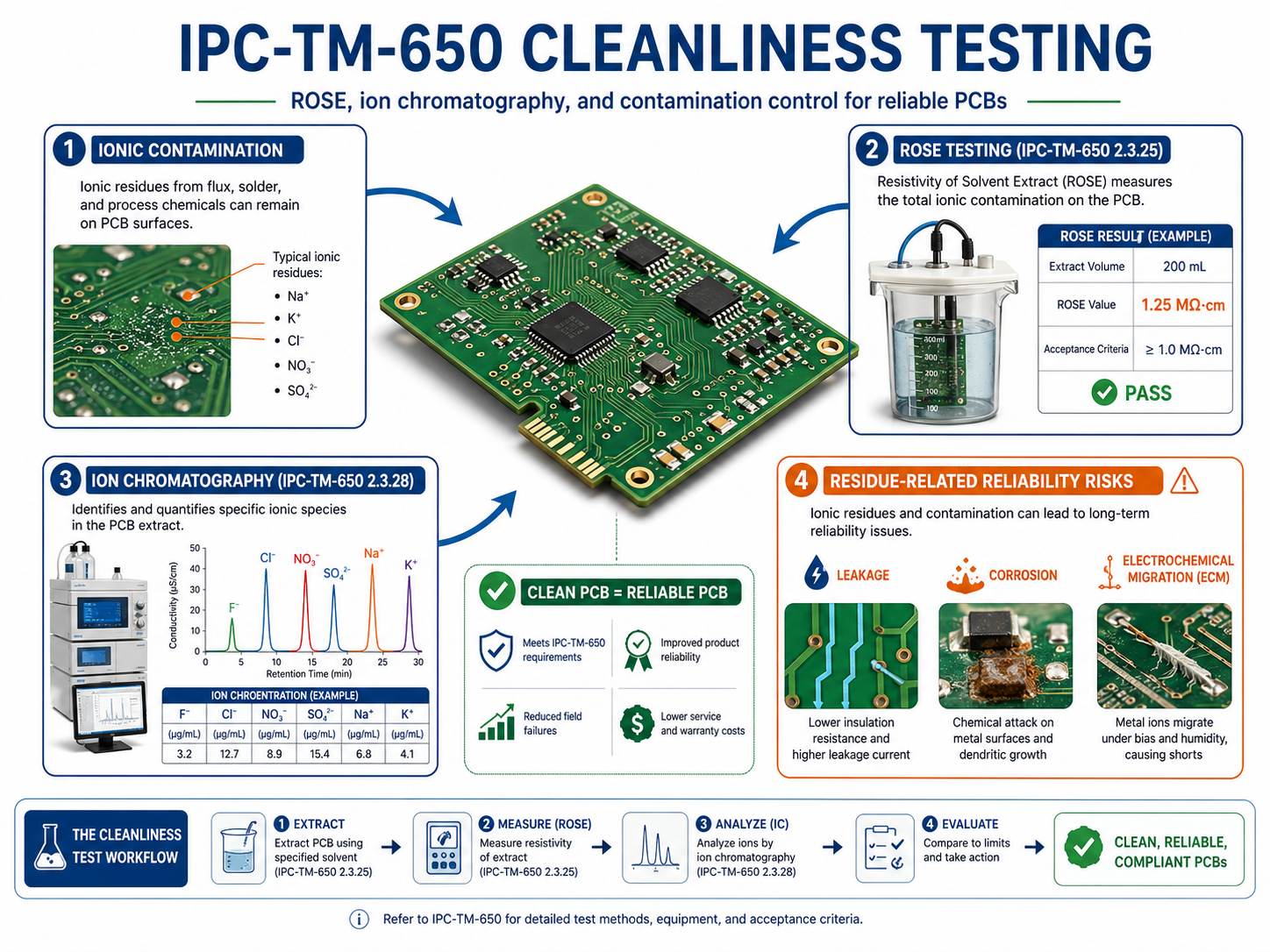
IPC-TM-650 Cleanliness and Ionic Contamination Testing

IPC TM 650 cleanliness tests help control residues from fabrication and assembly. These residues can come from flux, plating chemistry, cleaning agents, or handling.

IPC TM 650 ionic contamination testing is especially important for high-reliability PCBA. It helps measure mobile ionic material that may affect electrical performance.

Residues Create Risk

Cleanliness is easy to underestimate. A board can look clean under normal light and still carry harmful residues. Therefore, visual inspection alone is not enough.

In particular, ionic residues can absorb moisture. Then they may form leakage paths between conductors. Over time, this can lead to corrosion or dendritic growth.

IPC TM 650 ionic contamination limits depend on the test method, product use, and customer requirement. So, engineers should define limits before production starts.

How EBest Circuit handles this: We review materials, flux type, cleaning process, and testing needs before PCBA production begins.

Cleanliness TopicWhat To DefineBest Time To Review
Flux chemistryNo-clean or washableBefore SMT setup
Cleaning processAgent and cycleBefore trial run
Ionic limitCustomer requirementBefore quotation
Sampling planLot and frequencyBefore mass build

Overall, cleanliness control works best when design, process, and inspection teams align early. This is more efficient than fixing failures later.

Common IPC-TM-650 Mechanical and Adhesion Tests

IPC-TM-650 mechanical tests help check whether the PCB can survive fabrication, assembly, and field handling. These tests can include peel strength, tape testing, and adhesion testing.

Engineers often search for ipc tm 650 tape test, ipc tm 650 adhesion test, and ipc tm 650 peel strength. These topics matter when copper, solder mask, or surface layers must stay stable.

Adhesion Affects Reliability

Adhesion is important because PCB layers work as a system. Copper must bond well to the laminate. Also, solder mask must stay attached through heat and cleaning.

For example, poor peel strength can affect heavy copper boards. It can also affect edge plating, press-fit zones, and high-current terminals.

On the other hand, a simple consumer board may not need the same test depth. The right test plan should match product risk, not just a checklist.

Test AreaUseful ForCommon Product Type
Peel strengthCopper bond checkPower and heavy copper PCB
Tape testSurface adhesion checkSolder mask and marking
Adhesion testLayer stability checkIndustrial and automotive PCB
Thermal stressHeat resistance checkReflowed PCBA

Most importantly, these tests should support the design goal. A strong test plan starts with your application, not with a random standard list.

IPC-TM-650 Solderability Test and Copper Foil Testing

IPC TM 650 solderability test methods help check whether PCB pads can accept solder properly. This matters during SMT, wave soldering, selective soldering, and manual rework.

Also, ipc-tm-650 thermal conductivity copper foil searches often relate to material behavior. Engineers may need copper data for power, thermal, or high-current designs.

Solderability Drives Yield

Solderability affects first-pass yield. If pads oxidize or the finish performs poorly, solder joints may look dull or incomplete. Then rework cost can rise.

For instance, ENIG, OSP, immersion silver, and HASL each need proper storage and process control. Therefore, surface finish choice should match your assembly path.

CheckWhat It SupportsTypical Concern
SolderabilityPad wettingPoor joint formation
Copper foilMaterial stabilityThermal or current load
Surface finishAssembly shelf lifeOxidation or handling
Thermal exposureReflow performanceDelamination or stress

In general, solderability review should happen before production. This is especially true when components have fine pitch, bottom termination, or high thermal mass.

IPC-TM-650 for Prototype and Low-Volume PCB Builds

IPC-TM-650 is not only useful for large production. It can also help prototype and low-volume PCB builds move faster with fewer surprises.

Prototype teams often change materials, stack-ups, finishes, or components. Because of this, they need fast engineering feedback before committing to a larger build.

Better Prototype Decisions

First, test data helps you compare design options. For example, you can review flatness risk on a thin board before assembly. Then you can adjust the stack-up or panel plan.

Next, cleanliness and SIR checks can support early reliability review. This is useful for medical, sensing, RF, and industrial products. These products often need stable field behavior.

Also, solderability review helps when your BOM includes fine-pitch ICs or hard-to-source parts. A small issue in surface finish can waste expensive components.

Prototype NeedHelpful IPC-TM-650 AreaPractical Outcome
Thin PCBBow and twistBetter SMT stability
Fine-pitch layoutCleanliness and SIRLower leakage risk
High-power boardCopper and adhesionStronger thermal design
New surface finishSolderabilityHigher assembly yield

As a result, prototype testing can reduce redesign time. It also helps your team decide what to control during the next production stage.

How EBest Circuit Supports IPC-TM-650 Based PCB Quality Control?

EBest Circuit supports IPC-TM-650 based quality control through engineering review, controlled fabrication, PCBA process planning, and traceable production data. We connect these steps before your order enters production.

However, we do not treat testing as a separate final step. Instead, we use test needs to guide DFM, material choice, process flow, and inspection planning.

1 Account Manager + 3 Engineers

Each project receives one account manager and three engineers. The team covers DFM review, process planning, and quality control. As a result, communication stays clear from RFQ to shipment.

DFM and BOM Review

We include a DFM pre-review report and BOM optimization list with every order. This helps you find layout, material, component, and process risks early.

Certified Manufacturing System

EBest Circuit works under ISO 9001, ISO 13485, IATF 16949, and AS9100D systems. Therefore, we can support medical, automotive, aerospace, and industrial electronics projects.

Own Factories and Supply Chain

We operate our own PCB factory and own PCBA factory. In addition, we work with more than 1,000 supply chain partners. This helps us control lead time, materials, and assembly flow.

Prototype to Volume Support

We support prototypes, small batches, and volume production. For PCBA prototypes, our typical turnaround is about 1.5 weeks from build to shipped tested boards.

Digital MES Traceability

Our digital MES supports fast material and batch traceability. In many cases, teams can trace key production data within 5 seconds. This helps regulated projects manage records better.

20 Years of PCBA Experience

EBest Circuit has 20 years of PCBA experience. We have served more than 10,000 engineers and 1,800 customers. Because of this, we understand both engineering detail and delivery pressure.

To get a quote, send your Gerber files and BOM to sales@bestpcbs.com. We respond with a DFM report and quote within 24 hours.
FAQs About IPC-TM-650 Test Methods

What is IPC-TM-650 used for in PCB manufacturing?

IPC-TM-650 is used to define test methods for PCB materials, solder mask, cleanliness, insulation resistance, bow and twist, adhesion, solderability, and other quality checks.

Is IPC-TM-650 required for every PCB order?

IPC-TM-650 is not needed for every basic PCB order. However, it is useful when your product needs stronger proof of reliability, process control, or material performance.

Which IPC-TM-650 test checks bow and twist?

Bow and twist are commonly linked with IPC-TM-650 method 2.4.22. This method helps check PCB flatness after fabrication or thermal stress.

How does ionic contamination affect PCBA reliability?

Ionic contamination can attract moisture and create leakage paths. As a result, it may reduce insulation resistance and affect long-term PCBA reliability.

Can EBest Circuit support prototypes with IPC-TM-650 based controls?

Yes. EBest Circuit supports prototypes, small batches, and volume builds with DFM review, process planning, PCBA testing, and traceability control.

How do I request IPC-TM-650 test support from EBest Circuit?

You can send your Gerber files, stack-up, drawings, and BOM to sales@bestpcbs.com. We will review the project and suggest suitable quality control steps.
You may also like

IPC-TM-650 PCB Test Methods Manual
Wednesday, April 29th, 2026

What Is the IPC-TM-650 Test Methods Manual?

IPC-TM-650 test methods manual is a collection of standardized test procedures used to evaluate printed circuit boards, PCB materials, assemblies, and connectors. It helps PCB manufacturers, quality engineers, and buyers use the same technical language when discussing cleanliness, plating quality, solder mask reliability, electrical insulation, environmental stress, and mechanical stability.

In simple words, IPC-TM-650 tells people how to test a PCB-related item. It does not always tell people whether the result is acceptable for every project. The pass/fail requirement often comes from customer specifications, IPC product standards, procurement documents, or industry-specific quality requirements.

For PCB production, IPC-TM-650 is often used for:

  • PCB cleanliness verification
  • Bow and twist measurement
  • Solder mask reliability testing
  • Microsection analysis
  • Surface insulation resistance testing
  • CAF resistance evaluation
  • Thermal stress and thermal shock testing
  • Material electrical and mechanical property checks
IPC-TM-650 PCB Test Methods Manual

Why Is IPC-TM-650 Important for PCB Manufacturing Quality?

IPC-TM-650 is important because it gives PCB manufacturers and customers a consistent way to verify quality. Without a shared test method, one supplier may test cleanliness in one way, another may use a different extraction method, and a customer may struggle to compare results fairly.

It supports quality control in several practical areas:

  • Process control: checking whether manufacturing steps remain stable from batch to batch
  • Failure analysis: identifying the possible cause of leakage, corrosion, delamination, or solder mask failure
  • Supplier qualification: checking whether a PCB supplier can meet reliability expectations
  • Design verification: confirming that stack-up, materials, hole structure, and solder mask choices fit the application
  • High-reliability production: supporting medical, automotive, aerospace, telecom, power electronics, and industrial control projects

A PCB factory that understands these testing methods can usually communicate better during DFM review, material selection, production validation, and quality troubleshooting.

What Test Categories Are Included in IPC-TM-650?

IPC-TM-650 covers multiple test categories, including visual, dimensional, chemical, mechanical, electrical, environmental, and connector-related test methods. These categories help users quickly find the right method for a specific quality concern.

IPC-TM-650 CategoryMain Test FocusPCB Manufacturing RelevanceTypical Examples
Visual Test MethodsInternal and external observationHelps inspect plating, holes, laminate structure, and visible defectsMicrosectioning, plated-through hole evaluation
Dimensional Test MethodsSize, thickness, flatness, hole positionHelps control board geometry and assembly fitBow and twist, thickness, hole location
Chemical Test MethodsResidues, contamination, chemical propertiesHelps evaluate cleanliness and process residuesROSE, ion chromatography, organic contamination
Mechanical Test MethodsStrength, adhesion, peel, material behaviorHelps validate copper adhesion, solder mask durability, and flexible material strengthPeel strength, adhesion, abrasion
Electrical Test MethodsResistance, dielectric strength, signal performanceHelps evaluate insulation, high-voltage behavior, and RF propertiesSIR, dielectric strength, impedance-related tests
Environmental Test MethodsHumidity, heat, thermal cycling, agingHelps predict long-term reliability under service conditionsThermal shock, CAF, moisture resistance
Connector Test MethodsConnector durability and electrical behaviorHelps validate connector-level reliabilityContact resistance, vibration, humidity

What Is IPC-TM-650 Cleanliness Testing?

IPC-TM-650 cleanliness testing evaluates contamination, ionic residues, flux residues, process chemicals, and other materials that may remain on a PCB or PCBA surface. In PCB manufacturing, cleanliness is closely linked to insulation resistance, corrosion resistance, electrochemical migration, and field reliability.

Cleanliness is especially important when a board works in:

  • High humidity
  • High voltage
  • High impedance circuits
  • Medical monitoring equipment
  • Automotive control modules
  • Industrial sensors
  • Telecom infrastructure
  • Aerospace or defense electronics

A small amount of ionic residue may not create an immediate failure during final electrical testing. However, when moisture, voltage bias, and time are added, residues can support leakage paths, dendritic growth, corrosion, and unstable electrical behavior.

What Is IPC-TM-650 Cleanliness Testing?

IPC-TM-650 includes methods related to cleanliness and insulation performance, including surface insulation resistance and bare board cleanliness by SIR in the approved environmental test method list.

Cleanliness-Related TestWhat It ChecksBest Used ForPractical Value
ROSE TestOverall ionizable surface contaminationRoutine process controlFast cleanliness screening
Ion ChromatographySpecific ionic species and concentrationFailure analysis and high-reliability projectsFinds contamination source more precisely
SIR TestInsulation behavior under humidity and electrical biasCleanliness validation under stressShows reliability impact of residues
Visual InspectionVisible residue, staining, white marks, process contaminationInitial quality screeningSimple but not enough alone
Process AuditCleaning chemistry, rinse quality, drying, handlingManufacturing controlHelps prevent repeat issues

What Is IPC-TM-650 2.3.25 ROSE Testing for PCB Cleanliness?

IPC-TM-650 2.3.25 ROSE testing is commonly used to evaluate ionizable surface contaminants on PCB or PCBA surfaces. ROSE stands for Resistivity of Solvent Extract. It gives a fast cleanliness indicator, often reported as sodium chloride equivalent per unit area.

ROSE testing is useful because it is fast, repeatable, and suitable for production monitoring. If a PCB factory needs to compare different batches, check a cleaning process, or monitor contamination trends, ROSE can provide a practical baseline.

However, ROSE testing has a limitation. It measures total ionizable contamination, but it does not identify every individual ion. For example, a high ROSE reading may suggest contamination, but it may not tell whether the issue comes from chloride, bromide, weak organic acids, sodium, plating chemistry, flux residue, or handling contamination.

That is why ROSE is often used as a process control tool, while ion chromatography is used when a more detailed contamination profile is needed.

Good use cases for ROSE testing include:

  • Routine PCB cleanliness monitoring
  • PCBA cleaning process validation
  • Supplier quality comparison
  • Batch-to-batch contamination trend review
  • Quick screening before deeper analysis

For high-reliability products, ROSE alone may not be enough. It should be combined with ion chromatography, SIR, process traceability, and application-specific acceptance criteria.

What Is IPC-TM-650 2.3.28 Ion Chromatography Testing?

Ion chromatography is a more detailed cleanliness analysis method because it can identify and quantify specific ionic species. While ROSE gives an overall contamination value, ion chromatography helps show what type of contamination is present.

This matters in real PCB failure analysis. A board may show leakage current, corrosion, or dendritic growth after field use. A general contamination number may confirm that residue exists, but it may not explain the source. Ion chromatography can help identify whether the residue is related to process chemistry, flux activators, handling, water quality, or environmental exposure.

Typical ions that may be evaluated include:

  • Chloride
  • Bromide
  • Sulfate
  • Nitrate
  • Sodium
  • Potassium
  • Weak organic acids
  • Other process-related ionic species

Ion chromatography is especially valuable for medical electronics, automotive electronics, aerospace electronics, high-voltage PCB, and precision sensor circuits. In these products, contamination is not only a cosmetic concern. It can become a long-term electrical reliability risk.

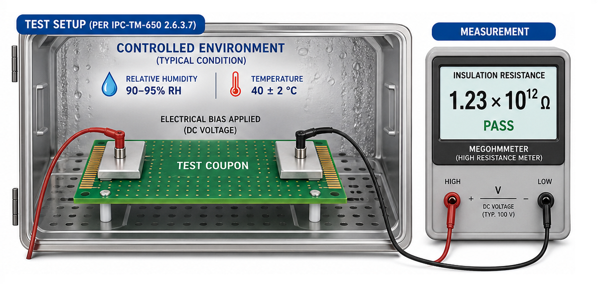
What Is IPC-TM-650 2.6.3.7 Surface Insulation Resistance Testing?

IPC-TM-650 2.6.3.7 surface insulation resistance (SIR) testing evaluates how well a PCB surface maintains electrical insulation under humidity, temperature, and electrical bias.

SIR testing is important because many contamination problems do not appear during normal room-temperature inspection. A board may pass final electrical testing immediately after production. But after exposure to moisture and voltage bias, residues may become conductive enough to reduce insulation resistance.

The official IPC TM-650 method list includes TM 2.6.3.7 as “Surface Insulation Resistance.”

IPC-TM-650 2.6.3.7 Surface Insulation Resistance Testing

In practical PCB production, SIR testing can help evaluate:

  • Whether a cleaning process is reliable
  • Whether solder mask materials maintain insulation under humidity
  • Whether residues create leakage paths
  • Whether no-clean flux residues are acceptable for the application
  • Whether high-impedance circuits will remain stable over time
  • Whether bare boards or assemblies are suitable for harsh environments

SIR should be considered when a PCB uses dense spacing, fine-pitch components, high voltage, no-clean processes, or sensitive analog circuits. It is also useful when qualifying a new solder mask, flux, cleaning process, or assembly supplier.

What Is IPC-TM-650 Bow and Twist Testing?

IPC-TM-650 bow and twist testing is used to evaluate PCB flatness. Bow refers to a board bending in a smooth curved shape, while twist refers to diagonal warpage where the corners are not on the same plane.

Flatness IssueWhat It Looks LikeMain Assembly RiskCommon Design or Process Cause
BowBoard bends like a shallow arcUneven solder paste transfer, placement offsetThin board, large panel, unbalanced copper
TwistBoard corners lift diagonallyConnector misalignment, BGA open jointsAsymmetric stack-up, laminate stress
Local WarpageOne area lifts or deformsFine-pitch soldering defectLocal copper imbalance or heat concentration
Panel WarpageFull production panel bendsRouting, depaneling, and handling issuesPanel size, material stress, thermal exposure

Bow and twist control is especially important for:

  • Thin PCB
  • Large-size PCB
  • HDI board
  • BGA assembly
  • Fine-pitch QFN and LGA packages
  • Press-fit connector boards
  • Automotive control boards
  • LED panels
  • Rigid-flex boards
  • Boards with uneven copper distribution
IPC-TM-650 Bow and Twist Testing

How Does Bow and Twist Affect PCB Assembly Reliability?

Excessive bow and twist can reduce assembly yield and long-term solder joint reliability. A PCB may still pass bare board electrical testing, but poor flatness can create serious problems during SMT assembly.

During solder paste printing, a warped board may not contact the stencil evenly. This can create insufficient solder paste in some areas and excess paste in others. During placement, small chip components may sit at different heights. During reflow, BGA or QFN packages may not maintain uniform contact with solder deposits.

The risks become more serious as component pitch becomes smaller. Common reliability problems caused by poor flatness include:

  • Open solder joints
  • Insufficient solder fillet
  • BGA non-wet open defects
  • Connector seating failure
  • Uneven mechanical stress after assembly
  • Housing fit problems
  • Local solder cracking during field vibration
  • Lower first-pass assembly yield

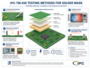
What Are IPC-TM-650 Testing Methods for Solder Mask?

IPC-TM-650 testing methods for solder mask help evaluate whether the solder mask can protect copper, maintain insulation, resist humidity, withstand thermal stress, and support long-term PCB reliability.

Solder mask is more than the green, blue, black, white, or red coating seen on a finished PCB. It protects copper traces, defines solderable areas, reduces solder bridging, and supports electrical insulation between conductors.

Poor solder mask performance can cause:

  • Solder bridging
  • Copper exposure
  • Mask peeling
  • Blistering
  • Cracking after reflow
  • Chemical attack from cleaning agents
  • Leakage under humidity
  • Electrochemical migration risk

The IPC TM-650 method list includes solder-mask-related methods such as solder mask dielectric strength, solder mask moisture and insulation resistance, solder mask thermal shock, solder mask hydrolytic stability, and solder mask resistance to electrochemical migration.

What Are IPC-TM-650 Testing Methods for Solder Mask?

How Is IPC-TM-650 Different from IPC-A-600, IPC-6012, and IPC-A-610?

IPC-TM-650 explains how to test, while other IPC documents often define what is acceptable. This difference is important because many buyers ask for “IPC standard” without knowing which document applies to the problem.

DocumentMain PurposeSimple ExplanationCommon Use
IPC-TM-650Test methods manualExplains how to perform testsCleanliness, SIR, bow and twist, solder mask tests
IPC-A-600Acceptability of printed boardsShows acceptable and non-acceptable bare board conditionsVisual inspection of bare PCBs
IPC-6012Performance specification for rigid PCBsDefines rigid PCB performance requirementsRigid board procurement and quality control
IPC-A-610Acceptability of electronic assembliesDefines PCBA workmanship acceptanceSMT assembly and solder joint inspection
Customer SpecificationProject-specific acceptance requirementDefines what the customer expectsSpecial reliability, materials, and reporting needs

Which IPC-TM-650 Test Methods Should You Choose for Your PCB Project?

The right IPC-TM-650 test depends on the product application, failure risk, PCB structure, operating environment, and customer requirement. A simple consumer board does not always need the same test plan as a medical, automotive, aerospace, or power electronics PCB.

The goal is not to order every possible test. The goal is to choose the tests that reduce the most relevant risk.

PCB Project TypeRecommended IPC-TM-650 Related Tests
HDI PCBMicrosectioning, CAF, SIR, thermal stress
Automotive PCBBow and twist, CAF, thermal cycling, SIR
Medical PCBCleanliness, ion chromatography, SIR, traceability report
RF PCBDk/Df, signal loss, dimensional stability
Power PCBDielectric strength, thermal stress, CAF, solder mask insulation
Rigid-Flex PCBPeel strength, bend reliability, microsectioning
Fine-Pitch SMT PCBBow and twist, solder mask registration, cleanliness
Solder Mask Critical PCBSolder mask dielectric strength, moisture resistance, thermal shock

For early-stage prototypes, microsectioning and basic dimensional checks may be enough. For mass production, the test plan should be more structured.

How Should You Read an IPC-TM-650 Test Report?

A useful IPC-TM-650 test report should show more than a pass/fail result. It should tell the reader which method was used, how the sample was prepared, what condition was applied, what result was measured, and how that result connects to the project requirement.

A weak report says, “Passed.” While a strong report explains the evidence.

When reviewing an IPC-TM-650 test report, check the following items:

  • Test method number
  • Test method revision
  • Sample name and part number
  • Production lot number
  • Material type and stack-up
  • Surface finish
  • Sample quantity
  • Test condition
  • Test duration
  • Equipment used
  • Calibration status
  • Measurement result
  • Acceptance criteria source
  • Photos, charts, or microsection images
  • Technician or engineer review
  • Final conclusion
  • Traceability information

For high-value PCB projects, test reports should be stored as part of the quality record. They may become important during customer audits, field failure review, design changes, and supplier qualification.

How to Choose a PCB Manufacturer with IPC-TM-650 Testing Capability?

A capable PCB manufacturer should understand IPC-TM-650 as a practical quality tool, not just a document name. The supplier should know which test applies, when it should be used, what result format is expected, and how the result affects manufacturing decisions.

When selecting a PCB supplier, ask specific questions. Do not only ask, “Can you make IPC-quality boards?”

Ask:

  • Can you provide IPC-TM-650 cleanliness testing support?
  • Can you measure bow and twist for thin or large-size boards?
  • Can you support solder-mask-related reliability testing when needed?
  • Can you provide microsection images for plated holes and microvias?
  • Can you support SIR or CAF testing for high-reliability products?
  • Can you link test results to production lots and material batches?
  • Can your engineering team review stack-up, copper balance, and process risks before production?
  • Can you explain whether a test result meets our project-specific requirement?

A strong supplier will not recommend unnecessary testing just to increase cost. Instead, the supplier should help match the test plan to the project risk.

For example, a simple 2-layer prototype may need only basic electrical test and visual inspection. A 12-layer automotive control board may need microsectioning, thermal stress, CAF review, cleanliness control, and bow and twist monitoring. A medical sensing PCB may require cleanliness testing, SIR validation, and strict traceability.

Testing capability is part of reliability. Engineering judgment is the other part.

FAQs About IPC-TM-650 Test Methods

1. What is the IPC-TM-650 test methods manual?

IPC-TM-650 test methods manual is a collection of standardized testing procedures for printed circuit boards, materials, assemblies, and connectors. It covers visual, dimensional, chemical, mechanical, electrical, environmental, and connector-related testing. It helps PCB manufacturers and customers evaluate quality using consistent methods.

2. Is IPC-TM-650 the same as IPC-A-600?

No. IPC-TM-650 explains how to perform PCB-related tests. IPC-A-600 focuses on the acceptability of printed boards. In simple words, IPC-TM-650 is about testing procedures, while IPC-A-600 is about inspection and acceptance of bare PCB conditions.

3. When should I request IPC-TM-650 testing from a PCB supplier?

You should request IPC-TM-650 testing when your PCB has reliability-sensitive requirements, such as high voltage, fine spacing, high impedance, medical use, automotive use, harsh environment exposure, strict cleanliness needs, or complex multilayer construction. It is also useful during supplier qualification and failure analysis.

4. Does every PCB project need IPC-TM-650 testing?

Not every PCB project needs the full range of IPC-TM-650 testing. A simple prototype may only need basic inspection and electrical test. High-reliability boards, dense HDI boards, medical electronics, automotive electronics, power boards, and RF boards often need a more complete test plan.

You may also like