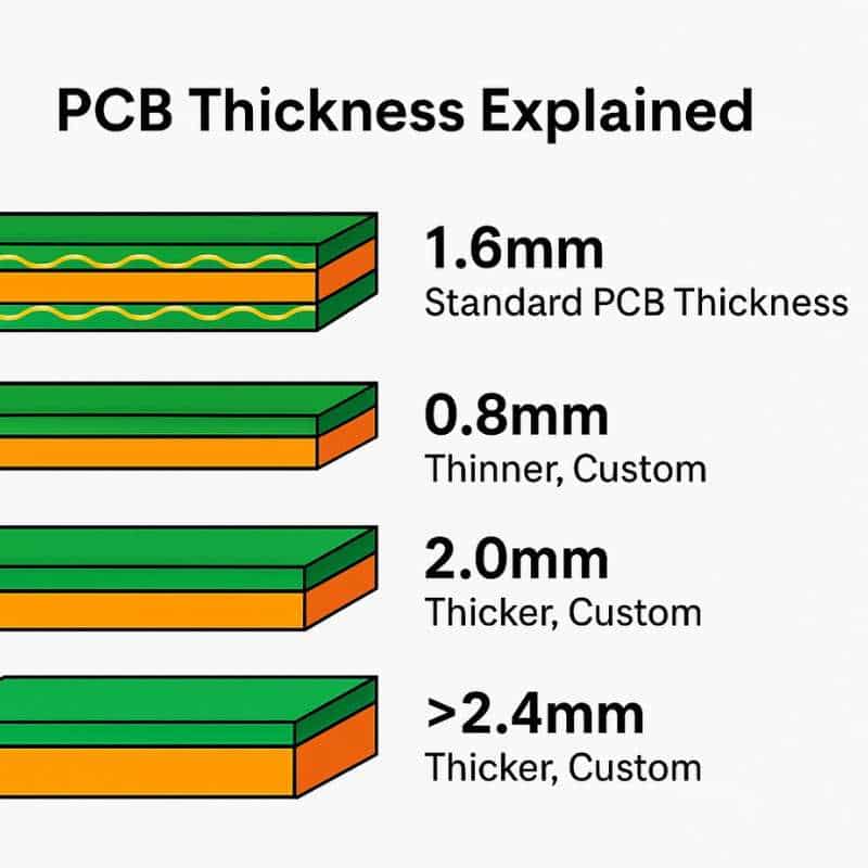
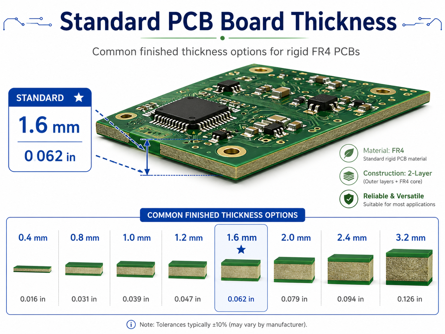
Standard PCB board thickness is commonly 1.6mm, also written as 1.57mm or 0.062 inch. This thickness is widely used for 2-layer, 4-layer, and many 6-layer FR4 PCBs because it provides a practical balance of mechanical strength, assembly compatibility, cost, and manufacturability.
However, PCB thickness can also range from 0.2mm to 3.2mm or more depending on product size, layer count, copper weight, impedance control, connector fit, and application requirements. For example, a wearable device may use a 0.6mm PCB, while an industrial power control board may use 2.0mm or 2.4mm for better rigidity.
What Is the Standard PCB Board Thickness?
The standard PCB board thickness is usually 1.6mm, or about 0.062 inch. This is the most common finished thickness for rigid FR4 printed circuit boards used in industrial electronics, consumer products, control boards, communication devices, and general electronic assemblies.
In PCB manufacturing, “standard” does not mean every PCB must use this thickness. It means this value is widely available, easy to produce, compatible with many assembly processes, and accepted by most enclosure and connector designs.
Common PCB thickness options include:
| PCB Thickness | Inch Equivalent | Common Use |
|---|---|---|
| 0.2mm | 0.008 inch | Ultra-thin rigid PCB, special compact devices |
| 0.4mm | 0.016 inch | Thin electronics, compact modules |
| 0.6mm | 0.024 inch | Small consumer devices, handheld products |
| 0.8mm | 0.031 inch | Compact control boards, plug-in modules |
| 1.0mm | 0.039 inch | Space-limited electronics |
| 1.2mm | 0.047 inch | Medium-thin boards with better rigidity |
| 1.6mm | 0.062 inch | Most common standard PCB thickness |
| 2.0mm | 0.079 inch | Industrial control, stronger mechanical demand |
| 2.4mm | 0.094 inch | High-strength PCB, larger boards |
| 3.2mm | 0.126 inch | Heavy-duty power boards, backplanes |
For most standard FR4 boards, 1.6mm is a safe starting point. It is thick enough to resist bending in normal use, yet not so thick that it increases cost unnecessarily. It also works well with standard SMT assembly, through-hole components, mechanical supports, and many types of connectors.
Still, the best thickness should always match the product structure. A PCB for a small sensor cannot be selected the same way as a PCB for an inverter, a battery charger, or an automotive control module.
Why Is 1.6mm Considered the Standard PCB Thickness?
1.6mm became the most common PCB thickness because it offers a strong balance between strength, cost, and manufacturing convenience. It is thick enough for stable handling during fabrication and assembly, while still being economical for mass production.
For many engineers, 1.6mm is the default thickness unless there is a clear reason to change it.
You may keep 1.6mm when:
- The PCB is a normal 2-layer or 4-layer FR4 board.
- There is no strict enclosure height limit.
- The board needs general mechanical strength.
- The design uses common connectors or terminals.
- The project is cost-sensitive.
- There is no unusual impedance, bending, or thermal requirement.
You may choose another thickness when:
- The product must be very thin.
- The board must fit a special card-edge connector.
- The enclosure has tight mechanical limits.
- The PCB is large and needs more rigidity.
- The circuit carries higher current.
- The design needs a special impedance stackup.
- The PCB is used in automotive, aerospace, medical, or harsh industrial environments.
So, 1.6mm is not a rule. It is a practical default.
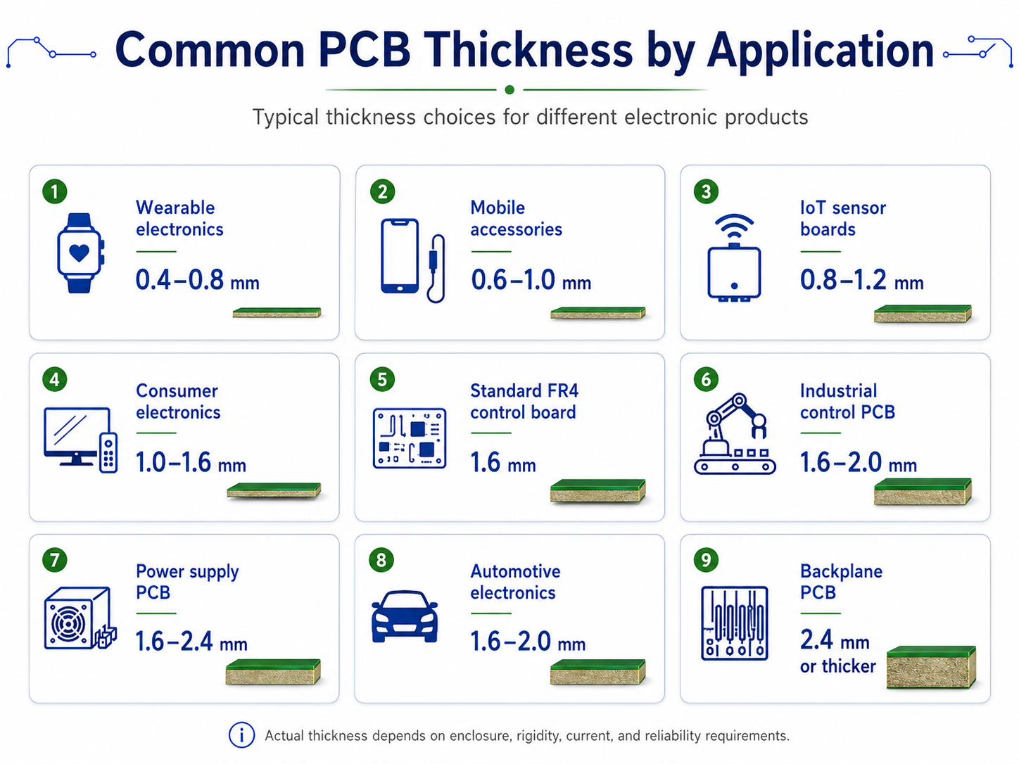
How Thick Is a PCB Board in Common Applications?
A PCB board can be as thin as 0.2mm or thicker than 3.2mm, depending on its application. The most common thickness for a general rigid PCB is 1.6mm, but thinner boards are popular in compact electronics, and thicker boards are used where strength, current capacity, or mechanical stability is important.
| Application | Common PCB Thickness | Engineering Reason |
|---|---|---|
| Wearable electronics | 0.4–0.8mm | Lightweight structure and thin product profile |
| Mobile accessories | 0.6–1.0mm | Compact enclosure and lower weight |
| IoT sensor boards | 0.8–1.2mm | Small size with moderate rigidity |
| Consumer electronics | 1.0–1.6mm | Cost, strength, and assembly balance |
| Standard FR4 control board | 1.6mm | Most common and economical option |
| LED control PCB | 1.0–1.6mm | Depends on housing and current demand |
| Industrial control PCB | 1.6–2.0mm | Better strength and connector support |
| Power supply PCB | 1.6–2.4mm | Higher current, larger components, better stability |
| Automotive electronics | 1.6–2.0mm | Vibration resistance and long-term durability |
| Backplane PCB | 2.4mm or thicker | Connector force and structural support |
For most projects, thickness selection starts with the mechanical design. The engineer should check the enclosure height, screw position, connector slot, component height, and assembly method first. After that, the electrical and thermal requirements should be reviewed.
A thin PCB can save space, but it may warp more easily during assembly. A thicker PCB improves rigidity, but it may increase cost and may not fit some connectors. A good PCB thickness decision balances both sides.
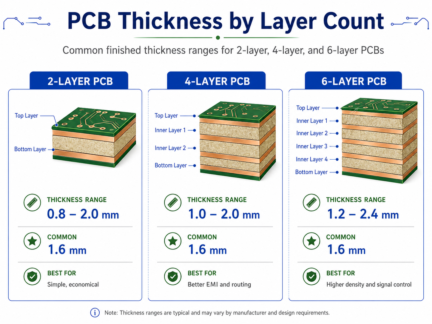
Standard PCB Thickness for 2-Layer Boards
The standard PCB thickness for a 2-layer board is usually 1.6mm. This is the most common choice for general FR4 double-sided PCBs used in control circuits, LED products, power adapters, small instruments, test boards, and electronic modules.
A 2-layer PCB has copper on the top and bottom layers. The base material between them is usually FR4 core. Because the structure is simpler than a multilayer PCB, 2-layer boards are easier to manufacture and usually offer more flexible thickness choices.
Common 2-layer PCB thickness options include:
| 2-Layer PCB Thickness | Typical Use |
|---|---|
| 0.4mm | Very thin electronics, compact module boards |
| 0.6mm | Small devices with limited space |
| 0.8mm | Plug-in modules, small control boards |
| 1.0mm | Compact products with better rigidity |
| 1.2mm | Medium-thin boards |
| 1.6mm | Standard 2-layer PCB thickness |
| 2.0mm | Stronger industrial or power boards |
| 2.4mm+ | Special mechanical or high-strength designs |
For most 2-layer PCB designs, 1.6mm works well. It gives enough stiffness for manual handling, soldering, connector insertion, and screw mounting. It also helps reduce bending during wave soldering or reflow soldering.
However, if the board is part of a small product, such as a handheld sensor, remote controller, or compact communication module, 0.8mm or 1.0mm may be more suitable. If the board carries large terminals, relays, or heavy components, 2.0mm may be a stronger option.
The main point is simple: 2-layer does not automatically mean 1.6mm. The product structure decides the best thickness.
Standard PCB Thickness for 4-Layer Boards
The standard PCB thickness for a 4-layer board is also commonly 1.6mm. Many 4-layer FR4 PCBs use 1.6mm because it supports a stable stackup, good mechanical strength, and practical cost control.
A 4-layer PCB usually has two outer copper layers and two inner copper layers. A common stackup may include:
- Top signal layer
- Inner ground layer
- Inner power layer
- Bottom signal layer
This structure improves routing density, EMI control, power distribution, and signal return path compared with a 2-layer board.
For 4-layer PCB thickness, the final value depends on:
- Core thickness
- Prepreg thickness
- Copper weight
- Inner layer copper
- Outer layer copper plating
- Solder mask thickness
- Surface finish
- Lamination pressure
- Impedance requirements
This is why 4-layer PCB thickness should not be selected only by habit. If the board has USB, Ethernet, RF, DDR, LVDS, HDMI, or other high-speed signals, the stackup should be checked before production. In these cases, dielectric thickness between signal and reference plane may be more important than the total board thickness.
| 4-Layer PCB Thickness | Suitable Situation |
|---|---|
| 0.8mm | Compact electronics with controlled stackup |
| 1.0mm | Thin multilayer modules |
| 1.2mm | Smaller boards with moderate rigidity |
| 1.6mm | Most common standard 4-layer PCB |
| 2.0mm | Stronger board or special structure |
| 2.4mm | Larger PCB, connector-heavy design |
For standard digital control boards, 1.6mm is usually practical. For compact devices, 1.0mm or 1.2mm may be better. For high-speed boards, the manufacturer should provide a stackup before fabrication.
Standard PCB Thickness for 6-Layer Boards
The standard PCB thickness for a 6-layer board is often 1.6mm, but 1.2mm, 2.0mm, and other custom thicknesses are also common depending on the design. A 6-layer PCB has more internal copper layers, so stackup planning becomes more important.
A 6-layer PCB may include signal layers, ground planes, power planes, and controlled impedance routing layers. Because more layers must fit into the same finished thickness, the manufacturer needs to carefully select core and prepreg materials.
A typical 6-layer board may use:
- Top signal layer
- Ground plane
- Inner signal layer
- Inner signal or power layer
- Power or ground plane
- Bottom signal layer
In many designs, the board can still be manufactured at 1.6mm. But the dielectric spacing, copper distribution, and lamination balance must be reviewed carefully. Poor layer balance may increase the risk of warpage, especially on larger boards.
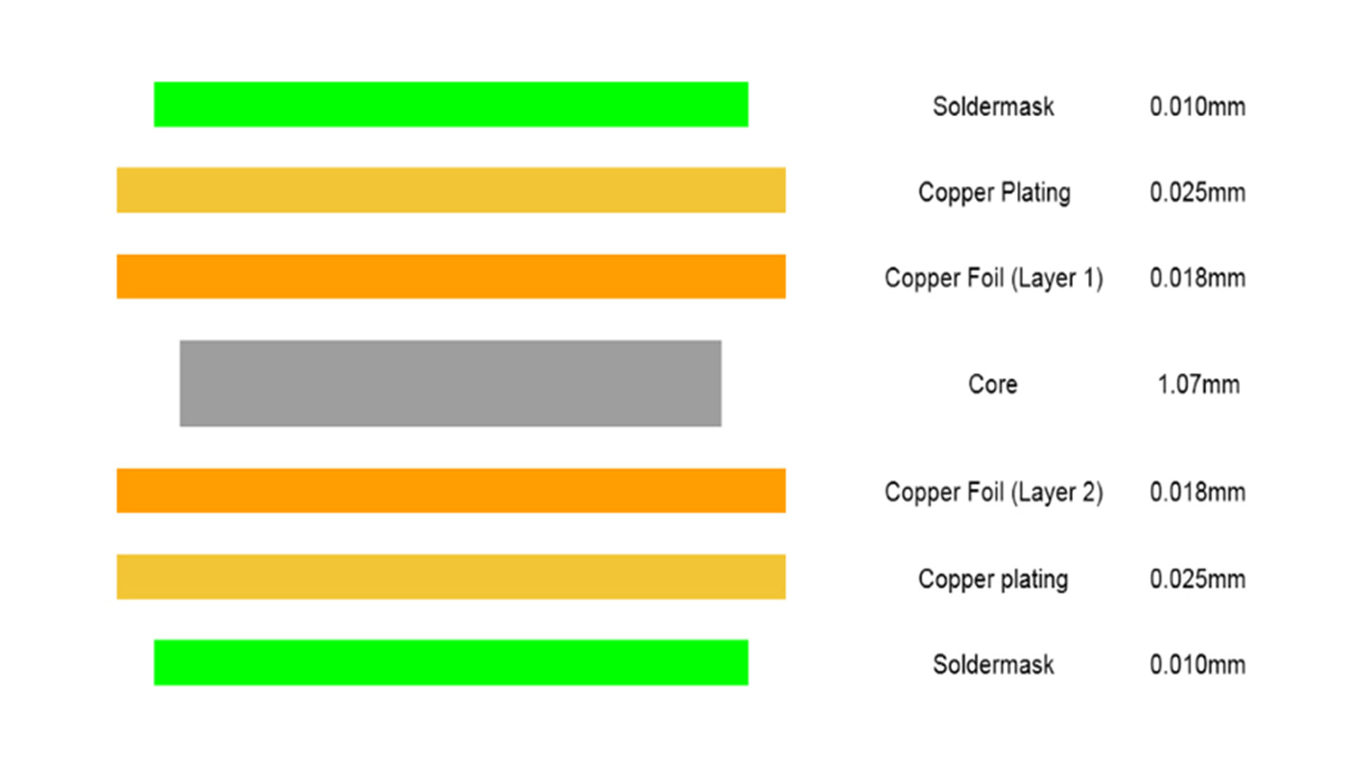
What Is the Standard Thickness and Weight of a Copper Layer on a PCB?
The standard copper thickness on a PCB is often 1 oz copper, which is about 35μm or 1.37 mil thick. Copper weight describes the copper thickness, not the total PCB thickness.
This is a common area of confusion. A 1.6mm PCB with 1 oz copper does not mean the whole board has 1 oz thickness. It means each specified copper layer uses copper foil with a weight of one ounce per square foot, which corresponds to around 35μm thickness before considering final plating effects.
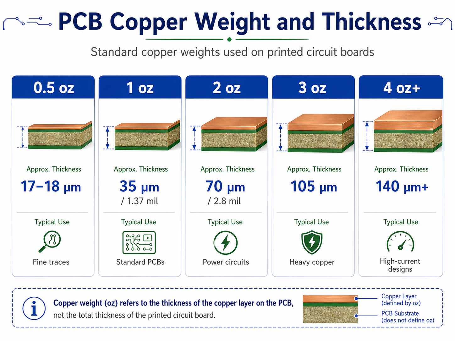
Common PCB copper weights include:
| Copper Weight | Approx. Copper Thickness | Typical Application |
|---|---|---|
| 0.5 oz | 17–18μm | Fine traces, compact signal boards |
| 1 oz | 35μm / 1.37 mil | Standard PCB copper thickness |
| 2 oz | 70μm / 2.8 mil | Power circuits, higher current paths |
| 3 oz | 105μm | Heavy copper PCB, motor control |
| 4 oz+ | 140μm+ | High-current and thermal applications |
Copper weight affects current capacity, trace width, etching accuracy, thermal behavior, and cost. A board with thicker copper can carry more current, but it also requires wider spacing and more careful manufacturing control.
For example, a power supply PCB may use 2 oz copper to handle higher current. A fine-pitch signal board may use 0.5 oz or 1 oz copper to support narrow traces and small spacing. A heavy copper PCB may use 3 oz or more for power conversion, battery systems, industrial equipment, and motor drives.
For multilayer PCBs, inner copper and outer copper may also be different. Outer layers usually gain additional copper thickness during plating, while inner layers remain closer to the original copper foil thickness. This should be considered when calculating current capacity and impedance.
How Does PCB Thickness Tolerance Affect Your Design?
PCB thickness tolerance is the allowed difference between the specified board thickness and the actual finished thickness. For example, a PCB ordered as 1.6mm may not measure exactly 1.600mm after fabrication. A reasonable manufacturing tolerance must be expected.
Thickness tolerance matters because PCB fabrication includes lamination, copper plating, solder mask coating, surface finish, and final routing. These processes all introduce small variations.
For ordinary control boards, standard tolerance is often acceptable. For card-edge products, backplanes, connectors, press-fit assemblies, or controlled-impedance boards, the tolerance should be defined clearly in the drawing or fabrication notes.
For example:
Finished PCB thickness: 1.6mm ±10%, FR4, 1 oz outer copper, ENIG surface finish, impedance control required.
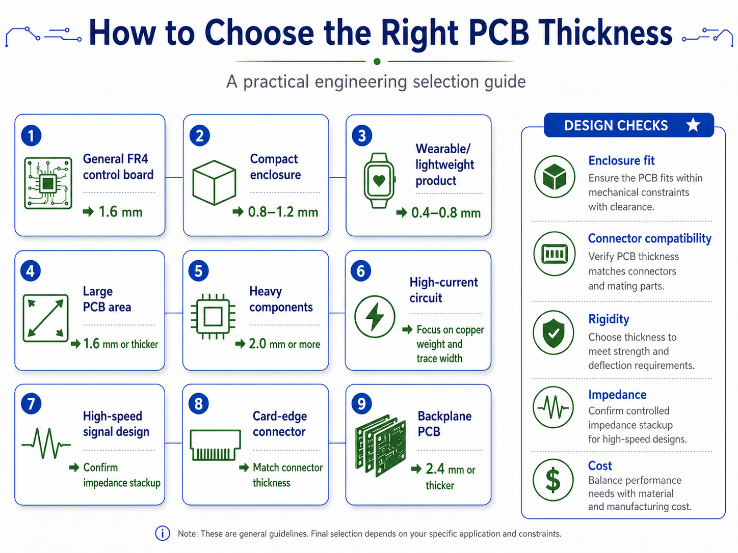
How Do You Choose the Right PCB Thickness for Your Project?
To choose the right PCB thickness, start with mechanical requirements first, then review electrical, thermal, and manufacturing needs. A good PCB thickness should fit the product, support the components, meet electrical performance, and remain manufacturable at a reasonable cost.
Here is a practical selection guide:
| Design Requirement | Recommended Direction |
|---|---|
| General FR4 control board | Use 1.6mm |
| Cost-sensitive prototype | Use standard 1.6mm when possible |
| Compact enclosure | Consider 0.8mm, 1.0mm, or 1.2mm |
| Wearable or lightweight product | Consider 0.4mm to 0.8mm |
| Large PCB area | Use 1.6mm or thicker to reduce bending |
| Heavy components | Consider 2.0mm or stronger mechanical support |
| High-current circuit | Focus on copper weight and trace width |
| High-speed signal design | Confirm impedance stackup before fabrication |
| Card-edge connector | Match the connector thickness requirement |
| Industrial environment | Consider 1.6mm, 2.0mm, or thicker |
| Automotive application | Check vibration, thermal, and reliability needs |
| Backplane PCB | Consider 2.4mm or thicker |
A simple rule can help:
- Use 1.6mm for standard designs.
- Use 0.8mm–1.2mm for compact electronics.
- Use 2.0mm or thicker for high-strength or heavy-component boards.
- Use a custom stackup when impedance, RF, thermal, or mechanical requirements are strict.
Thickness should also be discussed early with the PCB manufacturer. If the design uses special materials, controlled impedance, buried vias, blind vias, heavy copper, or HDI structures, the stackup should be confirmed before layout is finalized.
Can a PCB Thickness Calculator Give the Final Board Thickness?
A PCB thickness calculator can provide a useful estimate, but it cannot always give the final finished PCB thickness. Final thickness depends on actual laminate materials, prepreg flow, copper thickness, lamination pressure, solder mask, plating, surface finish, and manufacturing tolerance.
A calculator is helpful when you need early-stage estimation. For example, it can help you understand how core thickness, prepreg thickness, and copper layers may build up into the final board thickness. It can also support early stackup planning for 4-layer or 6-layer PCBs.
However, a calculator should not replace the manufacturer’s stackup confirmation.
This is especially true for:
- Impedance-controlled PCB
- High-speed digital PCB
- RF PCB
- HDI PCB
- Heavy copper PCB
- Rigid-flex PCB
- Automotive PCB
- Medical electronics PCB
- Aerospace PCB
For standard 2-layer FR4 boards, the thickness is usually easier to predict. For multilayer boards, the actual lamination result is more complex. Prepreg may compress during lamination, resin may flow into copper gaps, and copper distribution may influence final thickness.
The safest process is:
- Choose a target finished thickness.
- Define copper weight.
- Define layer count.
- Share impedance requirements if any.
- Ask the PCB manufacturer to provide a stackup.
- Review the stackup before final layout.
- Confirm tolerance before mass production.
A PCB thickness calculator is a planning tool. The approved manufacturing stackup is the production reference.
What PCB Board Sizes and Thicknesses Are Commonly Available?
Standard PCB board sizes do not mean every PCB has one fixed size. In PCB manufacturing, board size is usually customized according to the customer’s Gerber files. What manufacturers often standardize are material panel sizes, laminate thicknesses, copper weights, and production capability ranges.
For most FR4 PCBs, common finished thicknesses include:
| Common Finished Thickness | Typical Availability |
|---|---|
| 0.4mm | Available for thin rigid PCB |
| 0.6mm | Common for compact products |
| 0.8mm | Common for small modules |
| 1.0mm | Common for thin electronic products |
| 1.2mm | Common for medium-thin PCB |
| 1.6mm | Most standard PCB board thickness |
| 2.0mm | Common for industrial boards |
| 2.4mm | Available for stronger structures |
| 3.2mm | Used for special heavy-duty boards |
Board size also affects thickness choice. A small PCB can use thinner material more easily because it has less bending area. A large PCB may need 1.6mm or thicker material to reduce flexing during assembly and field use.
For example, a 30mm × 50mm sensor PCB can often use 0.8mm without major mechanical concerns. A 250mm × 180mm industrial control PCB may need 1.6mm or 2.0mm to remain stable. A backplane with multiple connectors may need even greater thickness.
How Does PCB Thickness Affect Cost and Lead Time?
PCB thickness affects cost and lead time mainly through material availability, lamination complexity, copper weight, and special processing requirements. Standard 1.6mm FR4 boards are usually easier to manufacture quickly because materials are widely available and production processes are mature.
Cost usually increases when:
- Thickness is non-standard.
- Material is not commonly stocked.
- Copper weight is heavy.
- Layer count is high.
- Impedance control is required.
- Tolerance is very tight.
- The board is very thin and large.
- The board is thick with small drilled holes.
For cost-sensitive designs, use common FR4 thickness and standard copper weight whenever possible. For performance-critical products, choose thickness based on engineering needs first, then optimize cost with the manufacturer.
How Should You Specify PCB Thickness in Fabrication Files?
You should specify PCB thickness as a finished board thickness, not only as a material preference. The fabrication drawing should include finished thickness, tolerance, copper weight, layer count, material type, surface finish, and any controlled impedance requirement.
A clear fabrication note helps prevent misunderstanding between the designer, buyer, and PCB manufacturer.
A basic example:
Material: FR4, finished thickness 1.6mm ±10%, 2 layers, 1 oz finished copper, green solder mask, white silkscreen, HASL lead-free finish.
A more advanced example:
Material: High Tg FR4, 4-layer PCB, finished thickness 1.6mm ±0.16mm, outer copper 1 oz finished, inner copper 0.5 oz, ENIG surface finish, controlled impedance required according to approved stackup.
For a high-speed PCB, the stackup document should be treated as part of the design. It should define each copper layer, dielectric layer, material type, dielectric thickness, copper weight, and target impedance.
Good communication at this stage can greatly reduce sample issues and improves production consistency.
FAQs About Standard PCB Board Thickness
1. What is the most common standard PCB board thickness?
The most common standard PCB board thickness is 1.6mm, also written as 1.57mm or 0.062 inch. It is widely used for FR4 2-layer, 4-layer, and many 6-layer PCB designs because it offers good strength, stable manufacturing, and broad assembly compatibility.
2. Is 1.6mm PCB thickness required for all PCB designs?
No, 1.6mm is common but not required for all designs. Thin products may use 0.4mm, 0.6mm, 0.8mm, or 1.0mm, while industrial control boards, power electronics, and backplanes may use 2.0mm, 2.4mm, or thicker boards.
3. What is the standard PCB thickness for a 2-layer board?
The standard PCB thickness for a 2-layer board is usually 1.6mm. However, 0.8mm and 1.0mm are also common for compact electronics, while 2.0mm may be used when the board needs stronger mechanical support.
4. Can I use a PCB thickness calculator for final production?
A PCB thickness calculator is useful for early estimation, but it should not be the only reference for final production. The final board thickness should be confirmed by the PCB manufacturer through an approved stackup and fabrication specification.
If your PCB project requires controlled thickness, special copper weight, impedance stackup, or manufacturability review, you can send your Gerber files, BOM, and technical requirements to EBest PCB for engineering support.
Contact: sales@bestpcbs.com