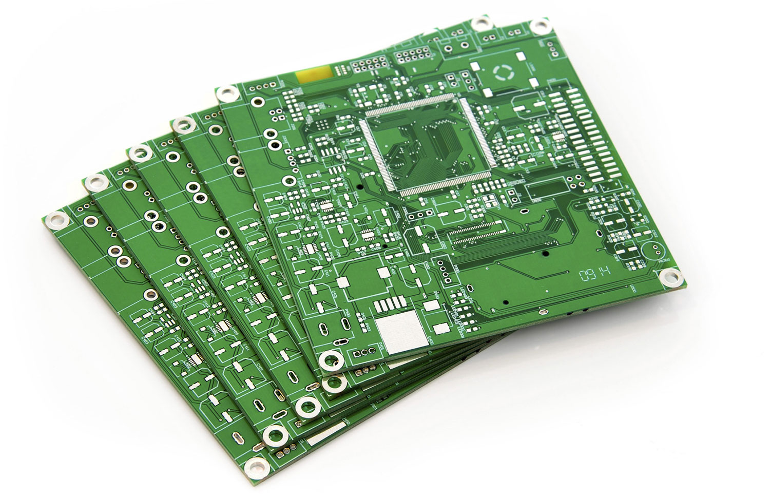
When it comes to PCB design for LED light, every detail—from thermal management to component layout—determines the performance, reliability, and lifespan of your LED products. Whether you’re designing for medical devices, aerospace lighting, or industrial equipment, getting PCB design for LED light right is non-negotiable. If you’re searching for a trusted PCB design for LED light manufacturer, look no further than EBestpcb. We deliver tailored solutions that solve your biggest design and production challenges, backed by expertise, certifications, and a proven track record in critical industries.

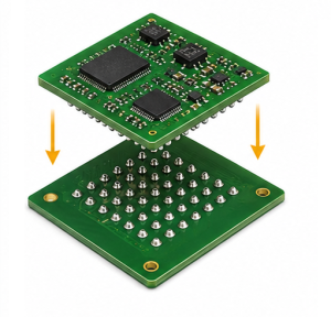
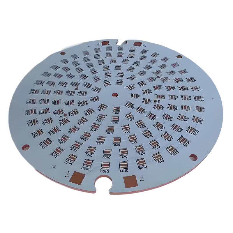
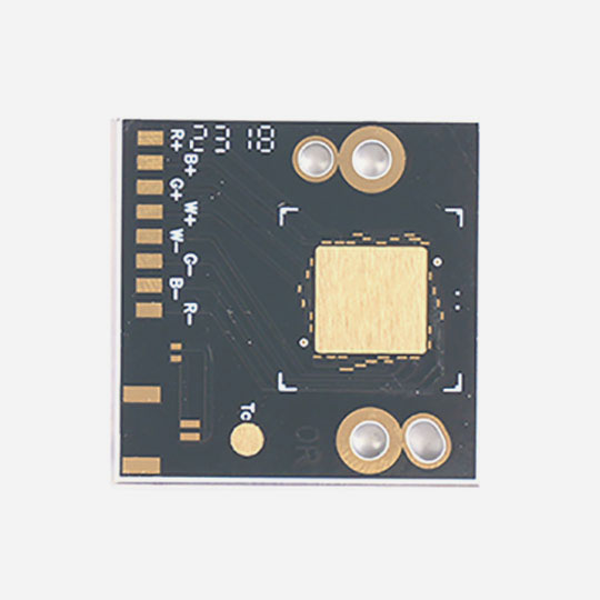
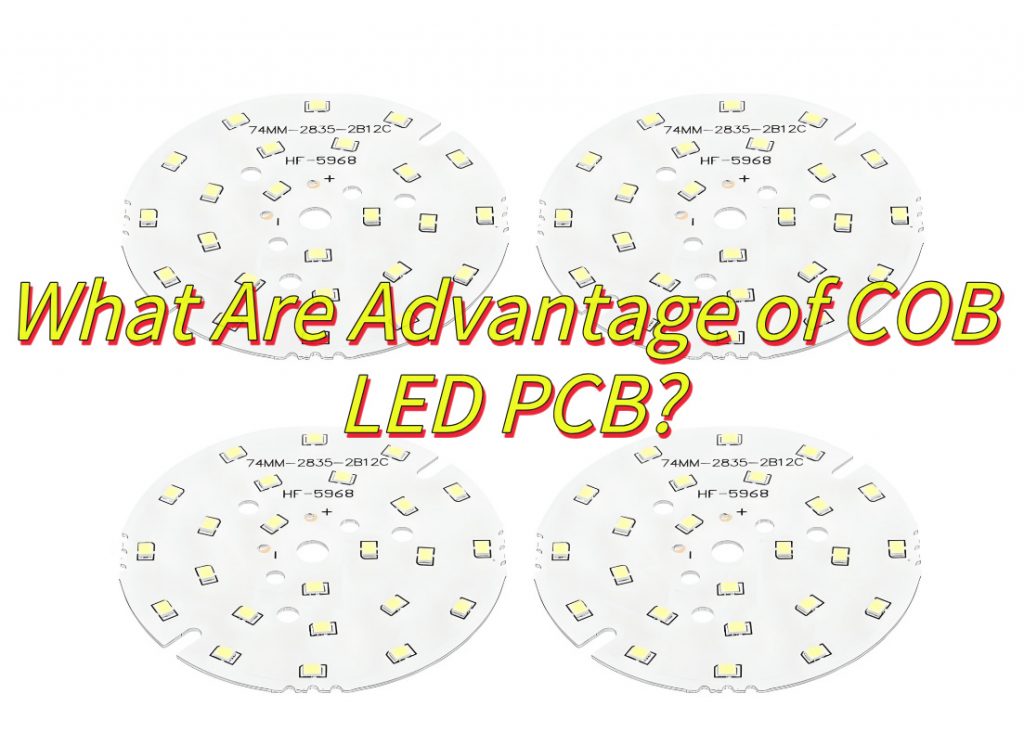
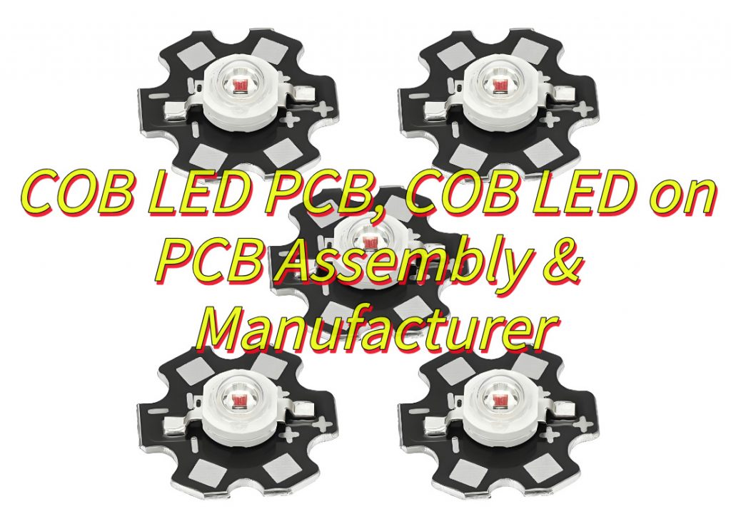
PCB Design for LED Light
Why Choose EBestpcb for Your PCB Design for LED Light Needs?
- Delivery Time: We prioritize fast, reliable lead times without compromising quality, ensuring your LED PCB projects stay on schedule—even for tight deadlines and complex designs.
- Quality Assurance: Our PCB design for LED light solutions undergo rigorous testing (including thermal cycling, AOI, and X-ray inspection) to ensure consistency, durability, and compliance with industry standards.
- Certifications: We hold global certifications that validate our commitment to excellence, including ISO 9001, ISO 13485 (for medical applications), IPC-A-610, and RoHS compliance.
- Cost-Effective Support: Enjoy free DFM (Design for Manufacturability) analysis to optimize your PCB design for LED light and reduce production issues, plus flexible low MOQ for prototyping and small-batch orders.
- Comprehensive Service: Our team of engineers provides end-to-end support—from initial design consultation and prototype development to mass production and post-delivery assistance.
Our PCB Design for LED Light Services
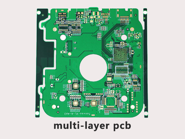
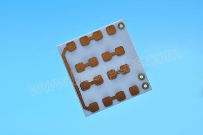
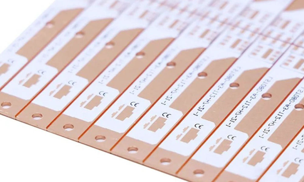
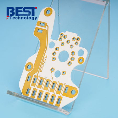
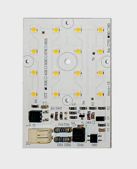
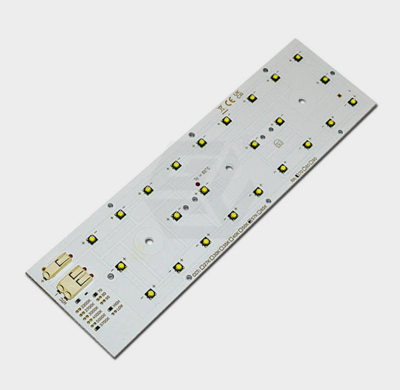
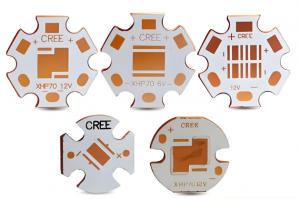
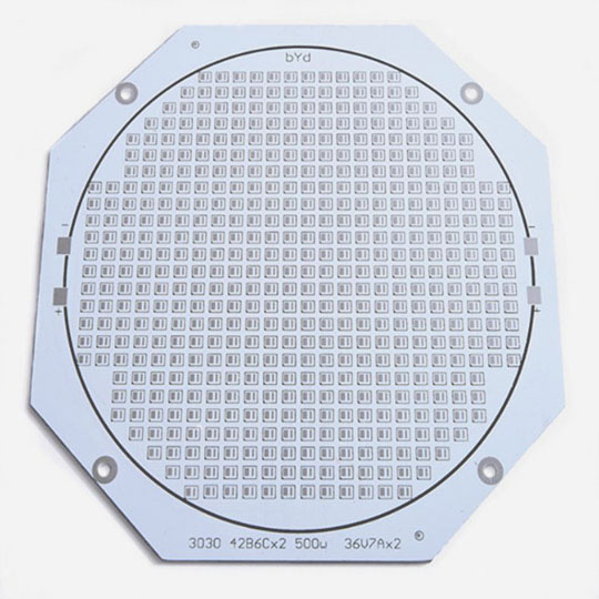
- Custom PCB design for LED light (single-layer, double-layer, and multi-layer PCBs) tailored to your specific LED application and industry requirements.
- Free DFM analysis to identify design flaws, optimize thermal performance, and ensure manufacturability for LED PCBs.
- Prototype development and testing for PCB design for LED light, including thermal testing, brightness consistency checks, and EMC compliance verification.
- Mass production of LED PCBs with strict quality control, including AOI, X-ray, and functional testing to guarantee reliability.
- Post-production support, including troubleshooting, design revisions, and technical guidance for LED PCB integration.
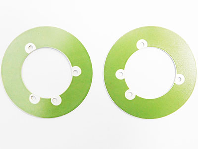
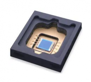
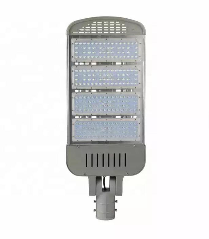
- Specialized solutions for high-power LED PCBs, medical LED devices, aerospace lighting, and industrial LED equipment.
Our Certifications for PCB Design for LED Light
- ISO 9001:2015 – Quality management system certification, ensuring consistent quality across all PCB design for LED light projects.
- ISO 13485:2016 – Certification for medical device components, validating our ability to design and manufacture LED PCBs for medical applications (e.g., surgical lighting, patient monitors).
- IPC-A-610 – Acceptability of Electronic Assemblies, ensuring our LED PCBs meet the highest industry standards for soldering and component placement.
- RoHS & REACH Compliance – Our PCB design for LED light solutions are free of hazardous substances, making them suitable for global markets.
- UL Certification – For LED PCBs used in commercial and industrial applications, ensuring safety and compliance with electrical standards.
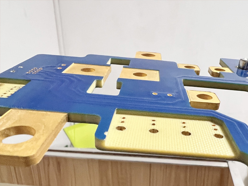
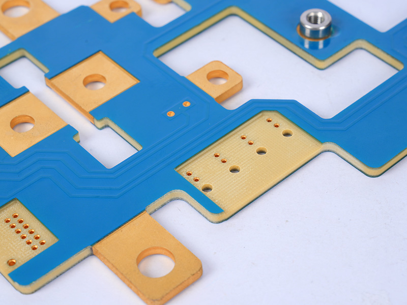
Our Manufacturing Capabilities for PCB Design for LED Light
| Capability | Specifications | Applicable LED PCB Types |
|---|---|---|
| Layer Count | 1-24 layers | All LED PCBs (low-power to high-power, medical, aerospace) |
| Copper Thickness | 0.5oz – 10oz (standard 2oz for high-power LED PCBs) | High-power LED PCBs, industrial LED equipment |
| Board Thickness | 0.2mm – 3.0mm | Medical LED devices, aerospace lighting, compact LED modules |
| Surface Finish | Immersion Gold, HASL (Lead-Free), OSP, ENIG | All LED PCBs (critical for solderability and corrosion resistance) |
| Minimum Line Width/Spacing | 3mil/3mil | High-density LED PCBs, medical and aerospace applications |
| Testing Capabilities | AOI, X-ray, Thermal Cycling (-40℃~125℃), EMC Testing | All LED PCBs (ensures reliability and compliance) |
Why Do LED PCB Designs Fail? We Solve Your Biggest Pain Points
Every PCB design for LED light project faces unique challenges—from overheating and brightness inconsistency to poor manufacturability and compliance issues. We’ve helped hundreds of clients overcome these pain points with tailored solutions, and we’re ready to help you too. Choose EBestpcb for PCB design for LED light that delivers reliability, performance, and peace of mind.
Pain Point 1: Overheating LED PCBs Leading to Premature Failure
Overheating is the #1 cause of LED PCB failure. LED chips generate significant heat, and poor thermal management in PCB design for LED light leads to high junction temperatures, faster light degradation, and component failure. Our solution: We integrate thermal-electric separation structures, high-thermal-conductivity materials (copper, ceramic substrates), and optimized thermal vias to reduce junction temperatures by 5-15℃, extending LED lifespan by up to 50%.
Pain Point 2: Brightness Inconsistency and Color Drift
Many LED PCBs suffer from uneven brightness or color drift, often due to poor current distribution or inadequate PCB layout. Our solution: We design PCB design for LED light with star-shaped power supply and grounding, independent constant current drivers (±3% precision), and optimized trace widths to ensure uniform current flow. For RGBW LED PCBs, we implement separate current control for each color channel to maintain color consistency.
Pain Point 3: Design Flaws Causing Manufacturability Issues
Even the best PCB design for LED light fails if it’s not manufacturable. Common issues include incorrect pad sizes, insufficient spacing, and poor thermal via placement. Our solution: We provide free DFM analysis to identify and fix these flaws early, ensuring your LED PCB design is optimized for our manufacturing processes—reducing rework, delays, and inconsistencies.
Pain Point 4: Non-Compliance with Industry Standards
Medical, aerospace, and industrial LED applications require strict compliance with industry standards (ISO 13485, IPC-A-610). Our solution: All our PCB design for LED light projects are developed in compliance with relevant standards, and we conduct rigorous testing to ensure your LED PCBs meet the requirements for your industry—whether it’s medical device safety or aerospace reliability.
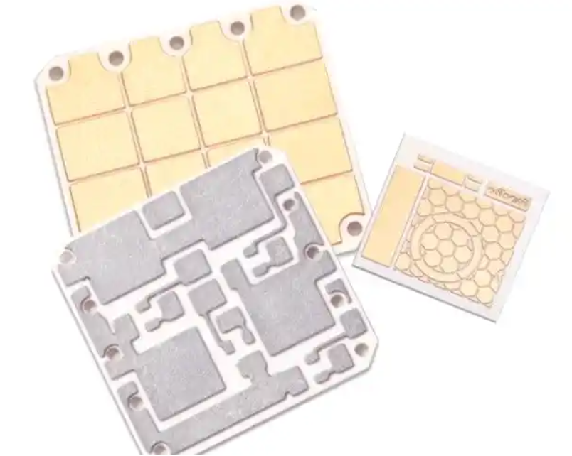
What Is the Best PCB Material for LED Light Design?
The best PCB material for PCB design for LED light depends on your application, power requirements, and environment. Below is a comparison of the most common materials to help you choose:
| PCB Material | Thermal Conductivity | Key Advantages | Best For |
|---|---|---|---|
| FR-4 | 0.3-0.5 W/m·K | Cost-effective, versatile, easy to manufacture | Low-power LED lights (e.g., household lighting) |
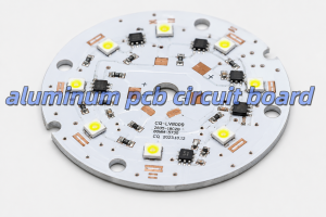
| Aluminum PCB | 1-2 W/m·K | Lightweight, good thermal dissipation, cost-effective | Commercial LED lights, industrial equipment lighting |
| Copper PCB | 3-4 W/m·K | Excellent thermal conductivity, high reliability | High-power LED lights (e.g., stage lights, industrial high-bay lights) |
| Ceramic (AlN) | 150-200 W/m·K | Ultra-high thermal conductivity, high insulation | Medical LED devices, aerospace lighting, precision optical LEDs |
How to Optimize Thermal Management for PCB Design for LED Light?
Thermal management is critical for PCB design for LED light—it directly impacts LED lifespan and performance. Follow these steps to optimize thermal management:
1. Choose the Right Substrate Material
For high-power LED PCBs, use copper or ceramic substrates (instead of FR-4) to improve heat dissipation. Ceramic substrates are ideal for medical and aerospace applications where reliability is critical.
2. Optimize Pad and Trace Design
Enlarge LED pads and use 2oz+ copper thickness to increase heat transfer. Add thermal vias (0.3mm diameter, 1.5mm spacing) under LED chips to channel heat to the back of the PCB.
3. Implement Thermal-Electric Separation Structures
For high-power applications, use thermal-electric separation PCBs to separate the circuit layer from the heat dissipation layer—reducing thermal resistance and preventing signal interference.
4. Add Heat Sinks or Thermal Pads
For extreme heat applications (e.g., industrial high-bay lights), integrate heat sinks or thermal pads to further reduce junction temperatures. Use thermal adhesive (Tg ≥ 150℃) for optimal heat transfer.
PCB Design for LED Light: Industry Case Studies
Medical Industry: Surgical LED Lighting PCB
A medical device manufacturer needed a PCB design for LED light for surgical lighting—requiring high brightness, low heat, and ISO 13485 compliance. We designed a 4-layer ceramic PCB with a thermal-electric separation structure, 3oz copper, and strict ESD protection. The result: LED junction temperature reduced by 12℃, brightness consistency improved by 95%, and full compliance with medical standards.
Aerospace Industry: Aircraft Cabin LED Lighting PCB
An aerospace client needed a lightweight, durable PCB design for LED light for aircraft cabin lighting. We used an aluminum substrate with an optimized trace layout, RoHS-compliant materials, and thermal cycling testing (-40℃~125℃). The PCB withstood 1000+ thermal cycles with no performance degradation, meeting aerospace reliability requirements.
Industrial Equipment: High-Power LED Industrial Light PCB
An industrial client required a PCB design for LED light for high-bay industrial lighting (100W+). We designed a copper substrate PCB with thermal vias, constant current drivers, and PWM dimming (2kHz+ to avoid flicker). The PCB achieved 85% power efficiency, reduced heat buildup by 30%, and lasted 50,000+ hours of continuous use.
FAQ: Common Questions About PCB Design for LED Light
1. What Causes LED PCB Overheating, and How to Fix It?
LED PCB overheating is caused by poor thermal management, inadequate copper thickness, or incorrect substrate material. To fix it: use high-thermal-conductivity substrates (copper/ceramic), add thermal vias, enlarge LED pads, and integrate heat sinks. Our PCB design for LED light team optimizes all these factors to keep junction temperatures within safe limits.
2. How to Ensure Brightness Consistency in LED PCB Design?
Brightness inconsistency stems from uneven current distribution. Fix it by using star-shaped power supply/grounding, independent constant current drivers for each LED or color channel, and optimized trace widths. We implement these strategies in every PCB design for LED light to ensure uniform brightness.
3. Which PCB Layer Count Is Best for LED Light Design?
The best layer count depends on your LED application. Low-power LED lights (household) use 1-2 layers. High-power, complex LED lights (medical/aerospace) use 4-8 layers to separate power, signal, and thermal layers. We recommend 4 layers for most industrial and medical PCB design for LED light projects for optimal performance.
4. Do LED PCBs Need ESD Protection, and Why?
Yes, LED PCBs need ESD protection. Static discharge can damage LED chips (hard or soft failure), leading to premature failure. We add TVS diodes and ESD protection circuits to all PCB design for LED light projects, especially for medical and aerospace applications where reliability is critical.
5. How to Optimize PCB Design for LED Light Manufacturability?
Optimize manufacturability by following DFM guidelines: use standard pad sizes, ensure adequate trace spacing (≥3mil), place thermal vias correctly, and avoid complex layouts. Our free DFM analysis for PCB design for LED light identifies and fixes manufacturability issues early, reducing rework and delays.
6. What Certifications Are Required for Medical LED PCB Design?
Medical LED PCB design requires ISO 13485 certification (for medical devices), IPC-A-610 (for electronic assemblies), and RoHS compliance. We ensure all our medical PCB design for LED light projects meet these certifications, plus any additional client-specific requirements.
Choose EBestpcb for Your PCB Design for LED Light Needs
Whether you’re designing LED PCBs for medical devices, aerospace lighting, or industrial equipment, EBestpcb is your trusted partner for high-quality, reliable PCB design for LED light solutions. We solve your biggest pain points, deliver on time, and ensure compliance with industry standards. If you need PCB design for LED light that combines performance, durability, and manufacturability, contact us today—we’re ready to bring your project to life.