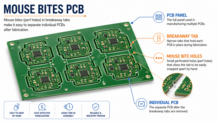
What Are Mouse Bites in PCB?
Mouse bites PCB refers to a PCB panelization method that uses small drilled holes on breakaway tabs to connect individual circuit boards inside a larger production panel. These small holes weaken the tab area, so the board can be separated more easily after fabrication, SMT assembly, inspection, or testing.
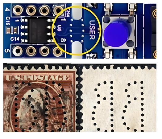
They are also called stamp holes, perforated tabs, breakaway holes, or PCB mouse bites. The name comes from the small semicircular marks left on the board edge after depaneling, which look similar to tiny bite marks.
In PCB manufacturing, most small boards are not always produced one by one. They are often placed into a larger panel to improve handling, assembly efficiency, and production stability. Mouse bites help keep each board connected during manufacturing while still allowing easy separation at the end.
This method is especially useful for:
- Small PCB boards
- Irregular-shaped PCBs
- Round or curved PCB outlines
- Boards with complex routing profiles
- PCBs that cannot use straight V-cut lines
- PCB panels that need strong temporary support during SMT assembly
For many projects, mouse bites are not just a small mechanical detail. They affect panel strength, edge quality, assembly stability, final appearance, and even product fit inside an enclosure.
Why Are Mouse Bites Used in PCB Panelization?
Mouse bites are used because they allow several individual PCBs to stay connected in one larger panel during manufacturing and assembly. This improves production efficiency, protects small boards from handling damage, and makes SMT assembly more stable.
Main reasons to use mouse bites include:
- They support small boards during automated assembly.
- They allow irregular PCB shapes to be panelized.
- They provide controlled breakaway points.
- They help reduce manual handling during production.
- They allow panel rails to be added for SMT machines.
- They are suitable when V-cut is not possible.
For example, if a PCB has a round shape, a curved edge, or a special mechanical outline, V-cut may not work because V-cut requires straight lines. In this case, tab routing with mouse bites is often a better choice.
How Do PCB Mouse Bites Work?
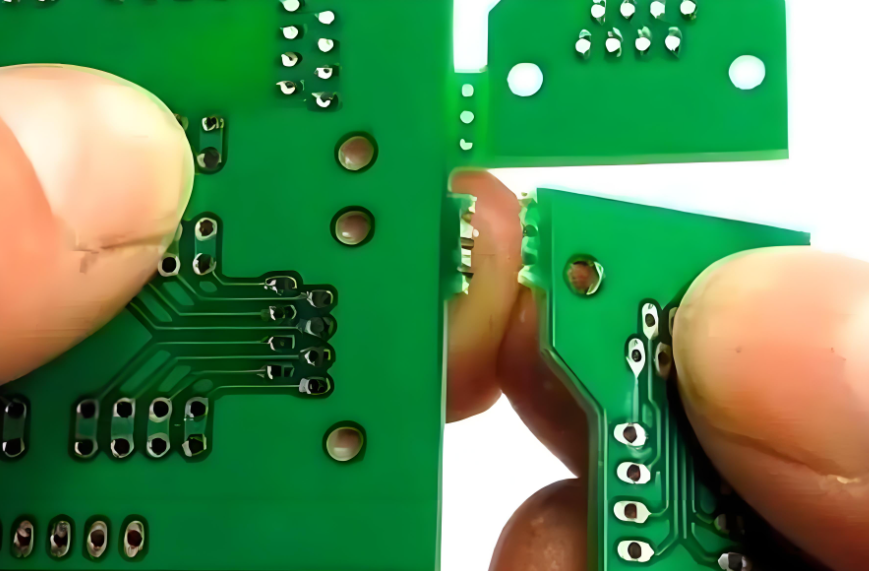
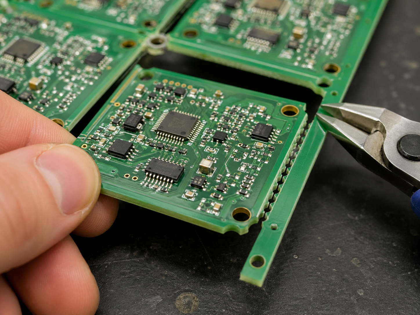
PCB mouse bites work by placing a row of small drilled holes through a breakaway tab. The tab holds the board in the production panel, while the holes reduce the mechanical strength of that tab. After assembly, the board can be snapped out along the weakened perforated area.
The process usually works like this:
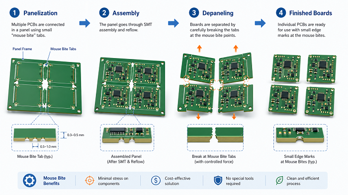
It looks easy, but it should pay much attention during the drilling process. If the holes are too large, the panel may become weak. If the holes are too small or too few, depaneling may become difficult. If the tab is placed near a connector, enclosure edge, or fragile component, separation stress may affect the final product.
A good mouse bite design balances three things:
- Panel strength during manufacturing
- Easy separation after assembly
- Acceptable board edge quality after depaneling
What Are the Standard Mouse Bites PCB Dimensions?
There is no single universal mouse bites PCB standard, because the best dimensions depend on board thickness, material, outline shape, component placement, panel size, and depaneling method. However, many PCB projects use small holes around 0.5 mm to 0.8 mm in diameter, with controlled spacing between holes.
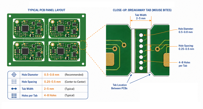
The table below gives practical reference values commonly used in PCB panelization.
| Design Item | Common Reference Range | Practical Design Note |
|---|---|---|
| Mouse bite hole diameter | 0.5–0.8 mm | Smaller holes usually leave finer edge marks, but may require more holes |
| Hole spacing | 0.25–0.5 mm edge-to-edge | Too close may weaken the tab too much |
| Holes per tab | 4–8 holes | Depends on tab width and board size |
| Tab width | 2–5 mm | Wider tabs improve panel strength but may need more cleanup |
| Tab quantity per board | 2–6 tabs | Larger or heavier boards need more balanced support |
| Distance from components | Preferably 2–3 mm or more | Keep away from brittle parts and solder joints |
| Board thickness consideration | 0.8–2.0 mm common range | Thicker boards may need adjusted tab design |
A practical example:
For a small 1.6 mm FR4 PCB, a designer may use 0.5 mm mouse bite holes, 5 or 6 holes per tab, and 2 to 4 tabs around the board. If the board has connectors on one side, the tabs should be placed away from that connector edge to protect the mechanical fit.
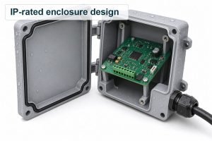
The safest approach is to provide the PCB supplier with the mechanical requirements, especially if the board edge must fit into a plastic housing, guide rail, slot, or metal enclosure.
Mouse Bites vs V-Cut: Which PCB Depaneling Method Is Better?
Mouse bites are better for irregular-shaped, small, or routed PCB designs, while V-cut is usually better for rectangular boards with straight separation lines. The best choice depends on board shape, edge quality requirement, assembly method, and production volume.
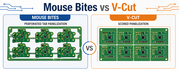
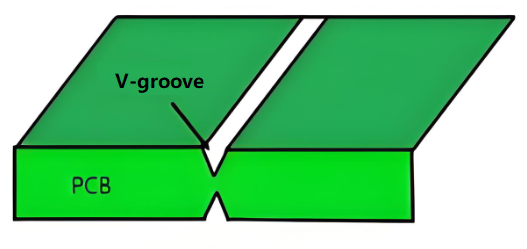
V-cut, also called V-score, creates a straight groove on both sides of the PCB panel. The board is later separated along that scored line. It is efficient and clean for simple rectangular arrays. However, it does not work well for curved outlines or complex board shapes.
Mouse bites use routed outlines and perforated tabs, so they are much more flexible for non-rectangular PCB designs.
When Should You Choose Mouse Bites for PCB Panels?
You should choose mouse bites when the PCB shape is not suitable for V-cut, when the board is small and needs support during assembly, or when the panel requires routed outlines with controlled breakaway tabs.
Mouse bites are commonly used when the PCB has:
- Irregular board outline
- Round or curved edges
- Small individual unit size
- Complex mechanical profile
- Nonlinear separation path
- Panel rails for SMT assembly
- Areas where V-cut cannot pass through
- Connectors or shapes that break a straight-line panel layout
For example, many wearable devices, sensor modules, LED control boards, communication modules, and compact IoT products use non-standard board outlines. These designs often benefit from mouse bite panelization.
However, mouse bites should be used carefully if the PCB edge is part of the final product appearance. If the board will be visible to the user, inserted into a tight enclosure, or mounted along a precise mechanical edge, the tab position should be reviewed early.
If the product requires a very smooth edge, mouse bites can still be used, but the board may need sanding, trimming, or secondary routing after separation.
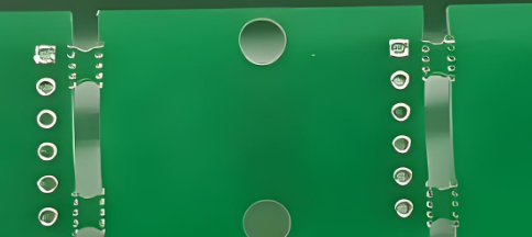
Where Should Mouse Bites Be Placed on a PCB?
Mouse bites should be placed on non-critical board edges, away from connectors, mounting features, fragile components, test points, and enclosure-fitting surfaces. Their position should support the panel during assembly while reducing stress during depaneling.
Placement is often more important than hole size. A technically correct mouse bite pattern can still cause problems if it is placed in the wrong area.
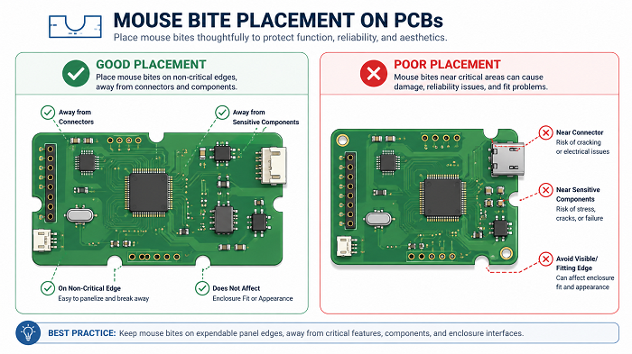
Better locations include:
- Non-visible edges
- Non-mating edges
- Areas without tight mechanical tolerance
- Edges away from connectors
- Areas with enough clearance from components
- Symmetrical positions around the board
Avoid placing mouse bites near:
- USB connectors
- Board-to-board connectors
- RF connectors
- Mounting holes
- Snap-fit housing edges
- Gold fingers
- Antenna keep-out areas
- Ceramic capacitors close to the edge
- BGA or fine-pitch ICs near the tab area
- Test pads or fixture contact points
If a board has only one suitable edge for tabs, the panel design may need extra support rails. For larger boards, tabs should be distributed evenly to avoid twisting during reflow or depaneling.
What Problems Can Poor Mouse Bite Design Cause?
Poor mouse bite design can cause rough board edges, difficult depaneling, cracked corners, damaged solder joints, weak panels, SMT instability, and mechanical interference during final assembly.
Most mouse bite problems are preventable. They usually come from poor tab position, incorrect hole size, too few tabs, too many holes, or lack of communication between PCB design and manufacturing.
| Problem | Possible Cause | Better Design Practice |
|---|---|---|
| Rough edge after separation | Holes too large or tab placed on visible edge | Move tabs to non-critical edges or use cleanup routing |
| Board cracking | Tab too strong or too close to board corner | Adjust tab width and add clearance |
| Difficult depaneling | Too few holes or holes too small | Increase hole count or optimize spacing |
| Weak panel during SMT | Too many holes or narrow tabs | Strengthen tabs or add support rails |
| Component damage | Tab placed near fragile components | Move tabs away from sensitive parts |
| Housing interference | Mouse bite burrs on fitting edge | Avoid tabs on enclosure-contact surfaces |
| Poor cosmetic appearance | Tabs placed on visible edge | Place tabs on hidden or internal edges |
| Test fixture conflict | Tab blocks test access | Review test point and fixture layout early |
The most common issue is edge roughness. Mouse bites naturally leave small marks because the board breaks along drilled perforations. This does not always affect electrical performance, but it can affect appearance, handling, and mechanical fit.
For consumer-facing products, medical device housings, handheld electronics, or precision-mounted assemblies, the edge requirement should be defined clearly before fabrication.
How Do Mouse Bites Affect PCB Assembly and Testing?
Mouse bites affect PCB assembly by controlling panel strength, board stability, depaneling stress, and handling efficiency. A good mouse bite layout helps the panel move smoothly through solder paste printing, pick-and-place, reflow soldering, AOI, X-ray inspection, ICT, and functional testing.
During SMT assembly, the PCB panel must stay flat and stable. If the tabs are too weak, the board may vibrate or move during handling. If the tabs are too strong, separation after assembly may require excessive force.
This is especially important for boards with:
- Fine-pitch ICs
- BGA packages
- Ceramic capacitors
- Tall connectors
- Heavy components
- Thin PCB materials
- Edge-mounted components
- High-density layouts
For assembled PCBs, depaneling should be done carefully. Snapping boards by hand may work for simple prototypes, but it can create mechanical stress on solder joints and components. For higher-value assemblies, controlled depaneling tools are safer.
How Can You Reduce Burrs After PCB Mouse Bite Depaneling?
You can reduce burrs after mouse bite depaneling by optimizing hole diameter, hole spacing, tab width, tab location, and post-processing method. The best strategy is to place mouse bites on non-critical edges and avoid using them on surfaces that require a smooth mechanical fit.
Mouse bite marks cannot always be completely avoided, but they can be controlled.
Practical ways to reduce burrs include:
- Use smaller mouse bite holes when suitable.
- Keep hole spacing consistent.
- Avoid placing tabs on visible product edges.
- Place the hole row closer to the waste side when possible.
- Use proper depaneling tools instead of twisting the board by hand.
- Add sanding or trimming after separation.
- Use secondary routing for high-precision edges.
- Choose V-cut if the board is rectangular and needs cleaner straight edges.
For boards that fit into housings, the safest approach is to mark the critical edges in the fabrication notes. A simple note such as “No mouse bites on enclosure-fitting edges” can prevent many mechanical problems.
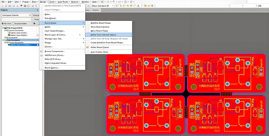
How to Prepare Mouse Bites PCB Files for Manufacturing?
To prepare mouse bites PCB files for manufacturing, provide complete panelization details, board outline data, tab locations, hole sizes, rail requirements, tooling holes, fiducial marks, and any special edge-quality requirements.
Many PCB issues come from incomplete fabrication notes. A manufacturer can create panelization based on standard rules, but they may not know which edge is cosmetic, which edge fits into a housing, or which area must avoid mechanical stress.
Recommended file information includes:
- Gerber files or ODB++ files
- Board outline layer
- Mechanical drawing or DXF file
- PCB thickness
- Surface finish requirement
- Single board size
- Finished panel size if required
- Mouse bite tab locations
- Hole diameter and hole spacing if specified
- SMT rail width
- Tooling holes
- Fiducial mark positions
- V-cut or routing instructions
- Critical edge notes
- Component keep-out areas near tabs
- Test fixture requirements
For PCB assembly projects, panel design should be confirmed before SMT production. Once components are mounted, changing tab positions becomes much more difficult.
How to Choose the Right PCB Supplier for Mouse Bite Panelization?
Choose a PCB supplier that can review your panelization design, check mouse bite placement, understand SMT assembly requirements, and provide practical DFM feedback before production. Mouse bites look simple, but they affect both fabrication and assembly quality.
A reliable supplier should not only drill the holes. They should help confirm whether the tab locations are safe, whether the panel is strong enough, and whether the edge quality matches the final product requirement.
EBest PCB supports PCB fabrication, PCB panelization review, PCBA assembly, component sourcing, testing, and engineering support for prototype and production projects. If your design uses mouse bites, V-cut, routing, or special panel rails, sharing the mechanical requirements early can help improve manufacturing stability and final board quality.
FAQs About Mouse Bites PCB
1. What are mouse bites in PCB?
Mouse bites in PCB are small drilled holes placed on breakaway tabs in a PCB panel. They are commonly used in tab-routing panelization, especially for small or irregular-shaped PCBs. After depaneling, the remaining edge may show small rough marks where the tab was broken away.
2. Are mouse bites the same as stamp holes?
Yes. In many PCB manufacturing discussions, mouse bites are also called stamp holes, perforated holes, breakaway holes, or tab holes.
3. Do mouse bites leave rough PCB edges?
Yes, mouse bites can leave small burrs or serrated marks after the PCB is separated from the panel. This is normal because the board breaks along the perforated tab area.
4. What is the typical mouse bite hole size?
A common mouse bite hole size is around 0.5 mm to 0.8 mm in diameter. The exact size depends on PCB thickness, material, tab width, panel strength, and the supplier’s process capability.
5. Is mouse bite better than V-cut?
Mouse bite is better for irregular-shaped, round, small, or routed PCBs. V-cut is usually better for rectangular boards that can be separated along straight lines.
6. Can mouse bites be used for assembled PCBs?
Yes. Mouse bites are widely used for PCBs that go through SMT assembly in panel form. They help keep the boards connected and stable during production.
However, the tabs should be placed away from fragile components, connectors, test points, and precision mechanical edges. After assembly, controlled depaneling is preferred to reduce stress on solder joints and components.
7. How many mouse bite tabs does a PCB need?
The number of tabs depends on board size, shape, thickness, and assembly requirements. Small boards may use two to four tabs, while larger or heavier boards may need more support points.
Can mouse bites affect PCB cost?
Yes, mouse bites can affect PCB cost slightly because they usually require routing, drilled perforations, and more detailed panelization work. However, they can also improve assembly efficiency for small or irregular boards.
For simple rectangular boards, V-cut may be more cost-efficient. For complex shapes, mouse bites often provide better manufacturability and handling stability.
Conclusion
Mouse bites PCB is a practical panelization method for small, irregular, and routed circuit boards. It uses small drilled holes on breakaway tabs to hold PCBs in a manufacturing panel and make separation easier after fabrication or assembly.
The key to good mouse bite design is balance. The panel must be strong enough for SMT assembly, but the tabs must also be easy to remove without damaging the board. Hole size, hole spacing, tab width, tab quantity, and tab location all influence the final result.
For most projects, mouse bites are a strong choice when V-cut is not suitable. They offer flexibility, support complex PCB outlines, and help improve production handling. Still, designers should pay attention to edge quality, component clearance, enclosure fit, and depaneling stress.
If your PCB requires mouse bites, V-cut, routing, special panel rails, or PCBA assembly support, EBest PCB can help review the design before production and provide practical manufacturing suggestions.
For PCB fabrication and assembly inquiries, contact: sales@bestpcbs.com.