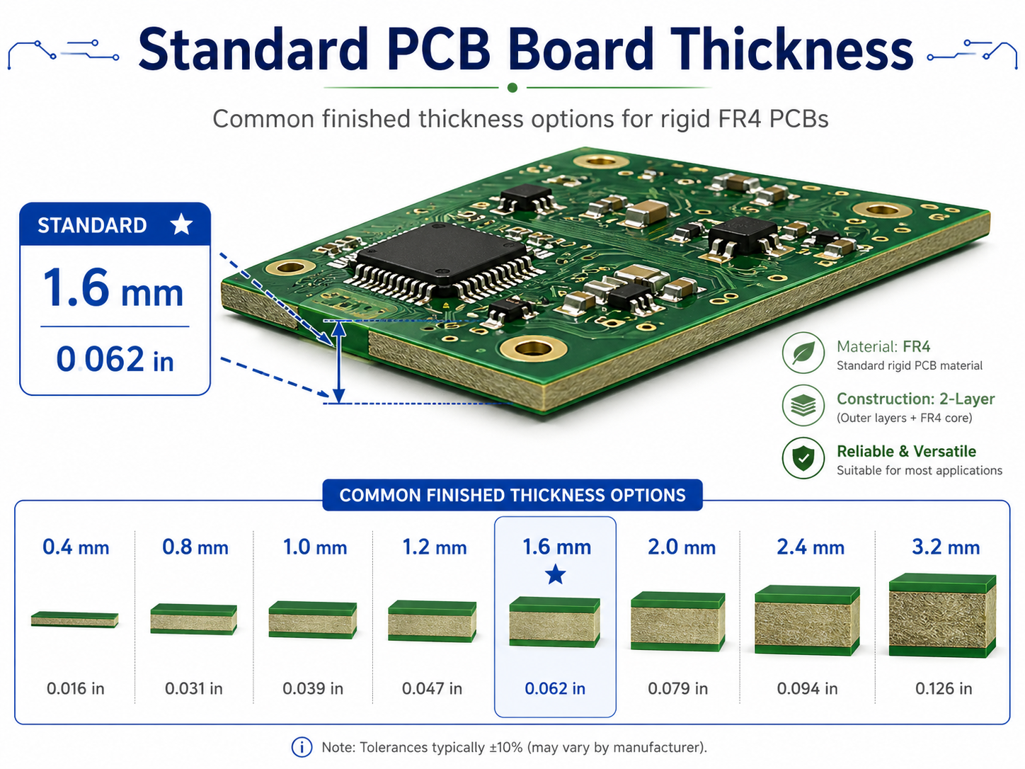
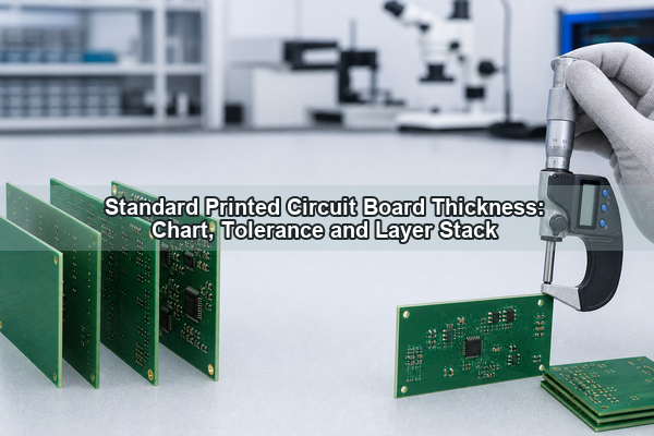
The most common standard printed circuit board thickness is 1.6 mm, approximately 0.062-0.063 inch or 62-63 mil. That value is a practical default for many rigid FR4 boards, but it is not a universal requirement. The correct finished thickness must also fit the layer stack, impedance geometry, connectors, enclosure, assembly process and mechanical load.
What Is the Standard Printed Circuit Board Thickness?
For a general-purpose rigid FR4 PCB, 1.6 mm is the conventional nominal finished thickness. The number developed from the older 1/16-inch laminate format, which equals 1.5875 mm. Modern fabrication drawings may state 1.57 mm, 1.60 mm, 0.062 inch or 0.063 inch, depending on the drawing convention and the fabricator’s standard material system.
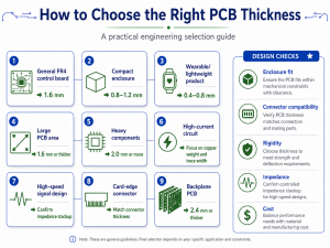
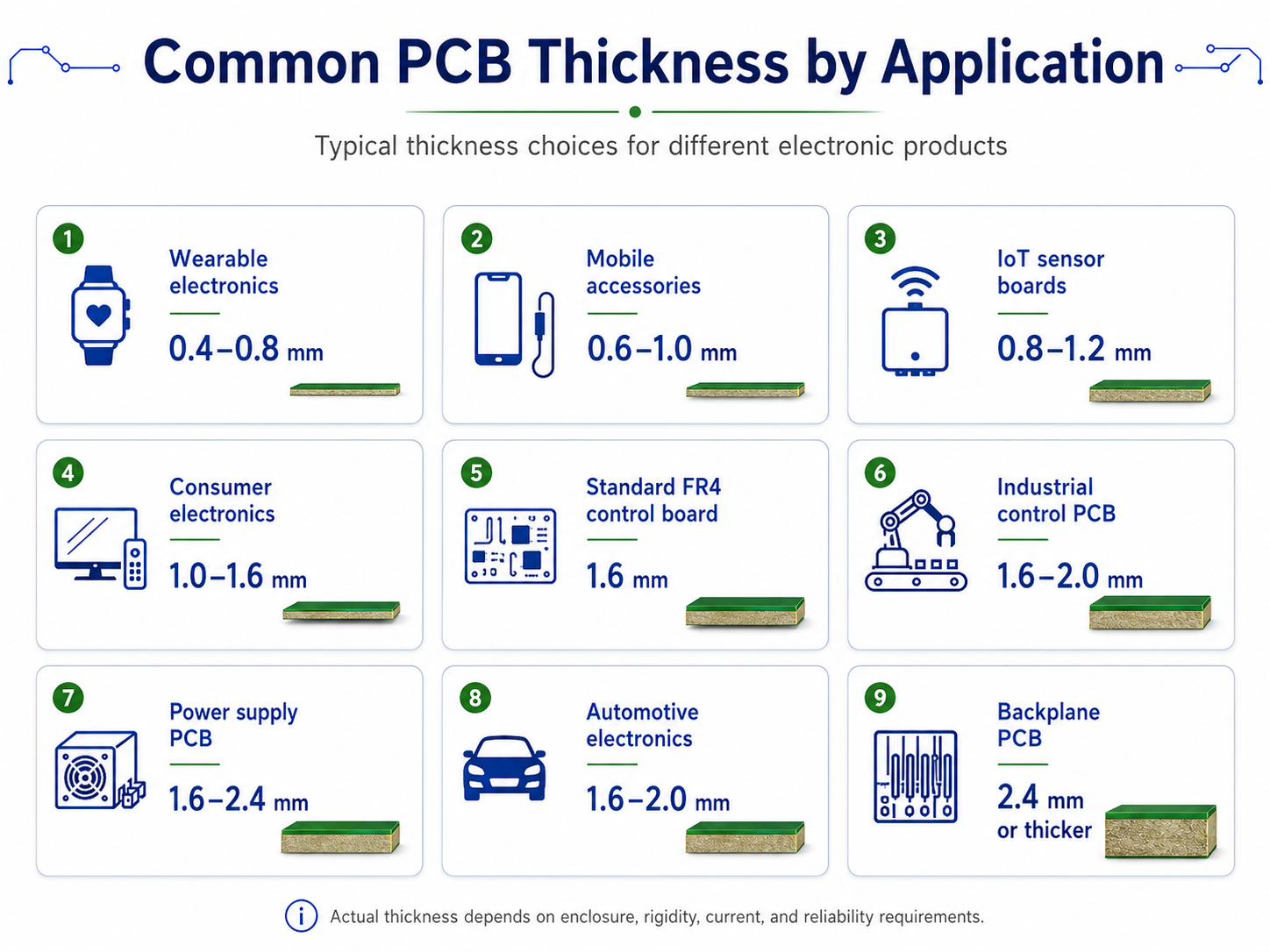
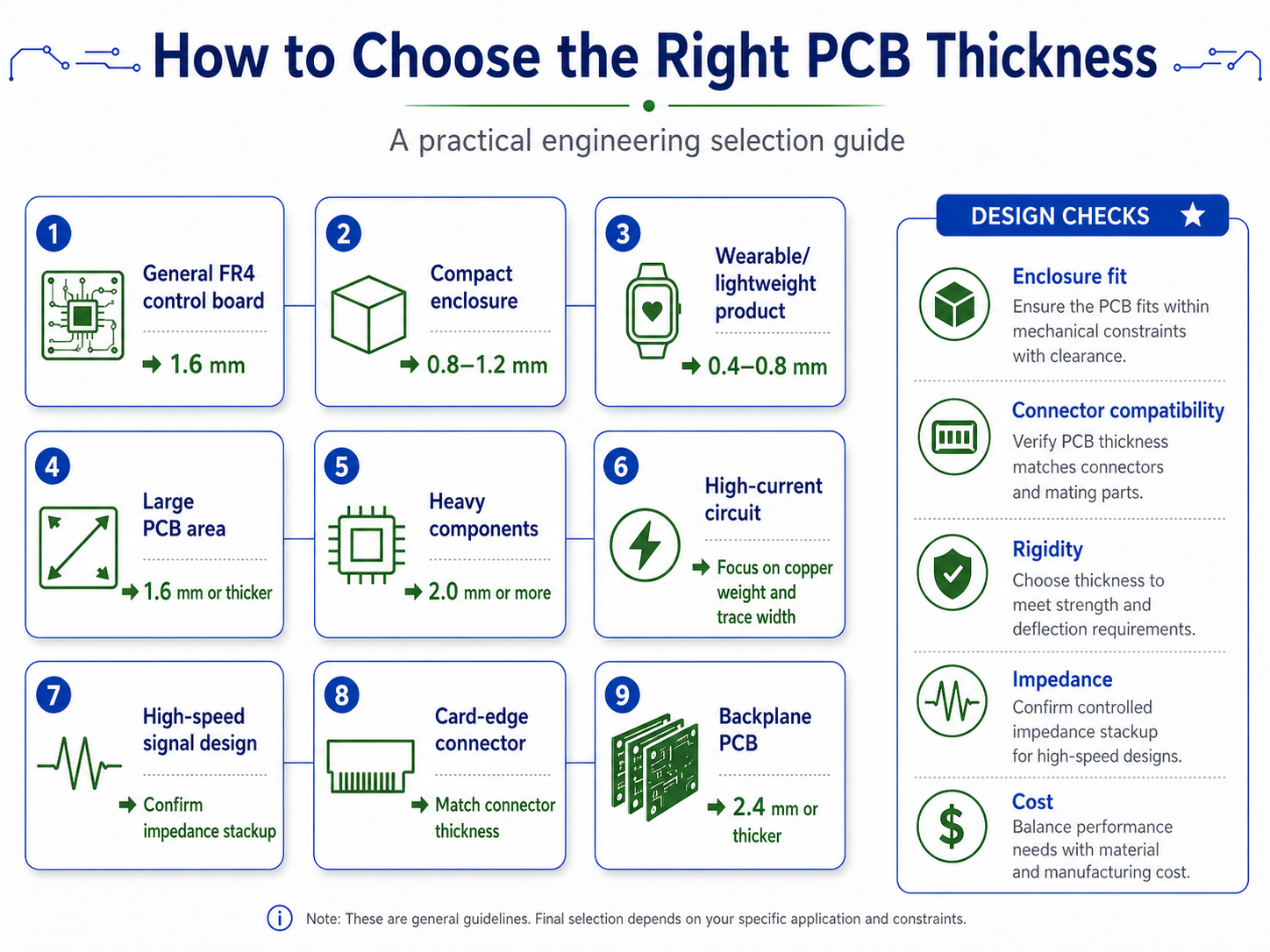
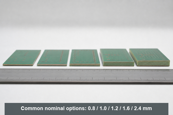
“Standard” means commonly stocked and routinely processed, not mandatory. A compact sensor module can use 0.8 mm to reduce height. A card-edge board may need 1.6 mm to fit its connector. A large industrial board may use 2.0 mm or 2.4 mm for stiffness. The stated value should therefore be treated as the nominal finished board thickness, with a separate tolerance that defines the acceptable production range.
Standard PCB Thickness Chart in Millimeters, Inches and Mils
The chart below converts common rigid-board thickness options. Availability varies with laminate family, layer count, copper weight and the fabricator’s stocked constructions.
| Nominal Thickness | Approx. Inches | Approx. Mils | Typical Design Direction |
|---|---|---|---|
| 0.4 mm | 0.016 in | 16 mil | Very thin rigid modules and space-limited assemblies |
| 0.6 mm | 0.024 in | 24 mil | Compact modules with controlled mechanical support |
| 0.8 mm | 0.031 in | 31 mil | Thin consumer, handheld and daughterboard designs |
| 1.0 mm | 0.039 in | 39 mil | Low-profile rigid boards with moderate stiffness |
| 1.2 mm | 0.047 in | 47 mil | Space-saving multilayer and control boards |
| 1.6 mm | 0.063 in | 63 mil | General rigid PCB default |
| 2.0 mm | 0.079 in | 79 mil | Boards needing additional stiffness or stackup space |
| 2.4 mm | 0.094 in | 94 mil | Industrial, connector or multilayer mechanical requirements |
| 3.2 mm | 0.126 in | 126 mil | Thick rigid boards and demanding mechanical structures |
These are nominal values rather than guaranteed measurements. The finished board is accepted against the thickness tolerance on the fabrication drawing. Conversion is also approximate because 1 mil equals 0.001 inch, while metric laminate systems are usually specified directly in millimeters.
Why Is 1.6 mm the Most Common PCB Thickness?
The 1.6 mm format remains common because material supply, fabrication tooling, connector geometry and product mechanics developed around the former 1/16-inch standard. It provides enough rigidity for many board sizes without making the assembly unnecessarily heavy. Fabricators can also build a wide range of 2-layer and multilayer constructions around this finished target.
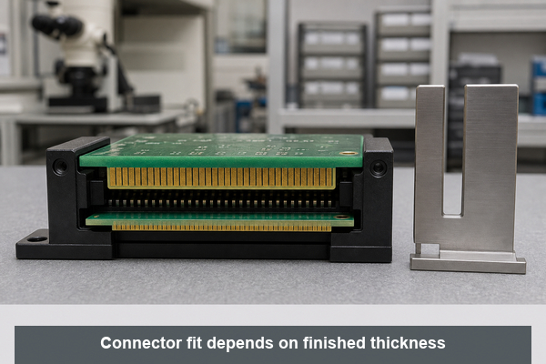
Component compatibility is another reason. Many card-edge connectors, board guides, standoffs and through-hole leads are designed around boards close to 1.6 mm. Using a thinner or thicker board can still be correct, but the mechanical interface must be checked rather than assumed. Press-fit hardware is especially sensitive because hole geometry, board thickness and pin engagement work together.
Cost is usually predictable at 1.6 mm because common cores and prepregs are readily available. A different thickness does not automatically make a PCB expensive, but a non-stock laminate construction, an unusual tolerance or a difficult multilayer build can require additional engineering and process control.
How Does PCB Thickness Differ From Copper Thickness?
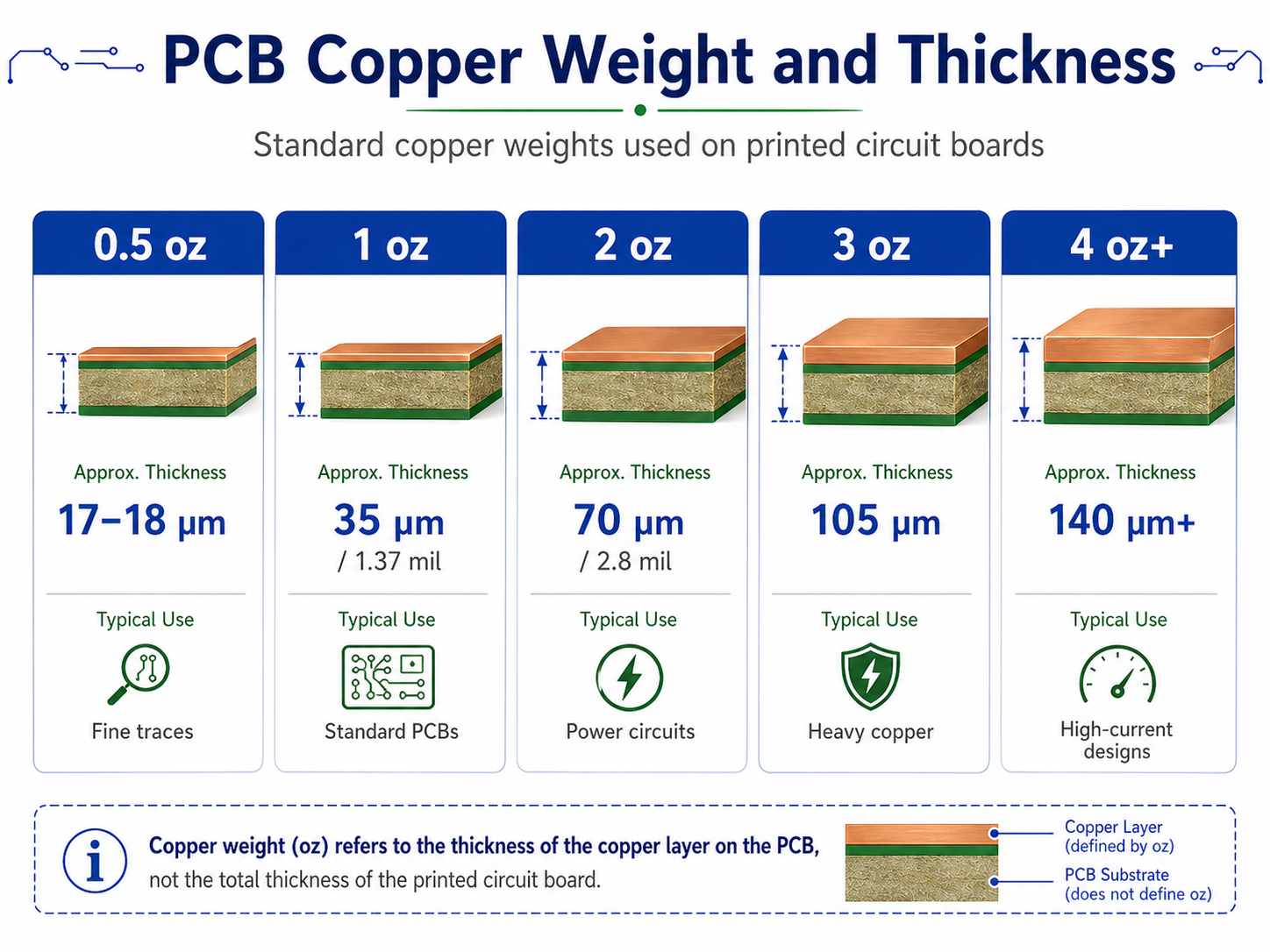
PCB thickness is the total finished board thickness. Copper thickness describes the conductor thickness on an individual layer. They are related in the stackup, but they are not interchangeable specifications.
| Specification | What It Measures | Common Units | Main Design Effects |
|---|---|---|---|
| Finished board thickness | Total rigid PCB construction | mm, inch, mil | Mechanical fit, stiffness, stackup space and drilling aspect ratio |
| Copper thickness | Copper on one conductor layer | oz/ft², µm, mil | Current capacity, trace resistance, etching and spacing |
| Dielectric thickness | Insulation between selected copper layers | mm, µm, mil | Impedance, coupling, isolation and layer spacing |
Typical nominal foil conversions are approximately 17 µm for 0.5 oz, 35 µm for 1 oz and 70 µm for 2 oz copper. Outer-layer finished copper may differ from starting foil because hole plating and pattern plating add copper. A 1.6 mm board can therefore use different copper weights without ceasing to be a 1.6 mm nominal board, provided the dielectric construction is adjusted accordingly.
A thick PCB is also not automatically a heavy-copper PCB. A 2.4 mm board with 1 oz copper is mechanically thick but does not use heavy copper. A 1.6 mm board with 4 oz copper is a heavy-copper design even though its total board thickness is conventional. The thick PCB board guide addresses the manufacturing effects of unusually thick rigid constructions.
What Determines Finished PCB Thickness?
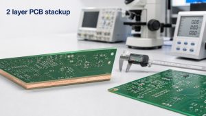
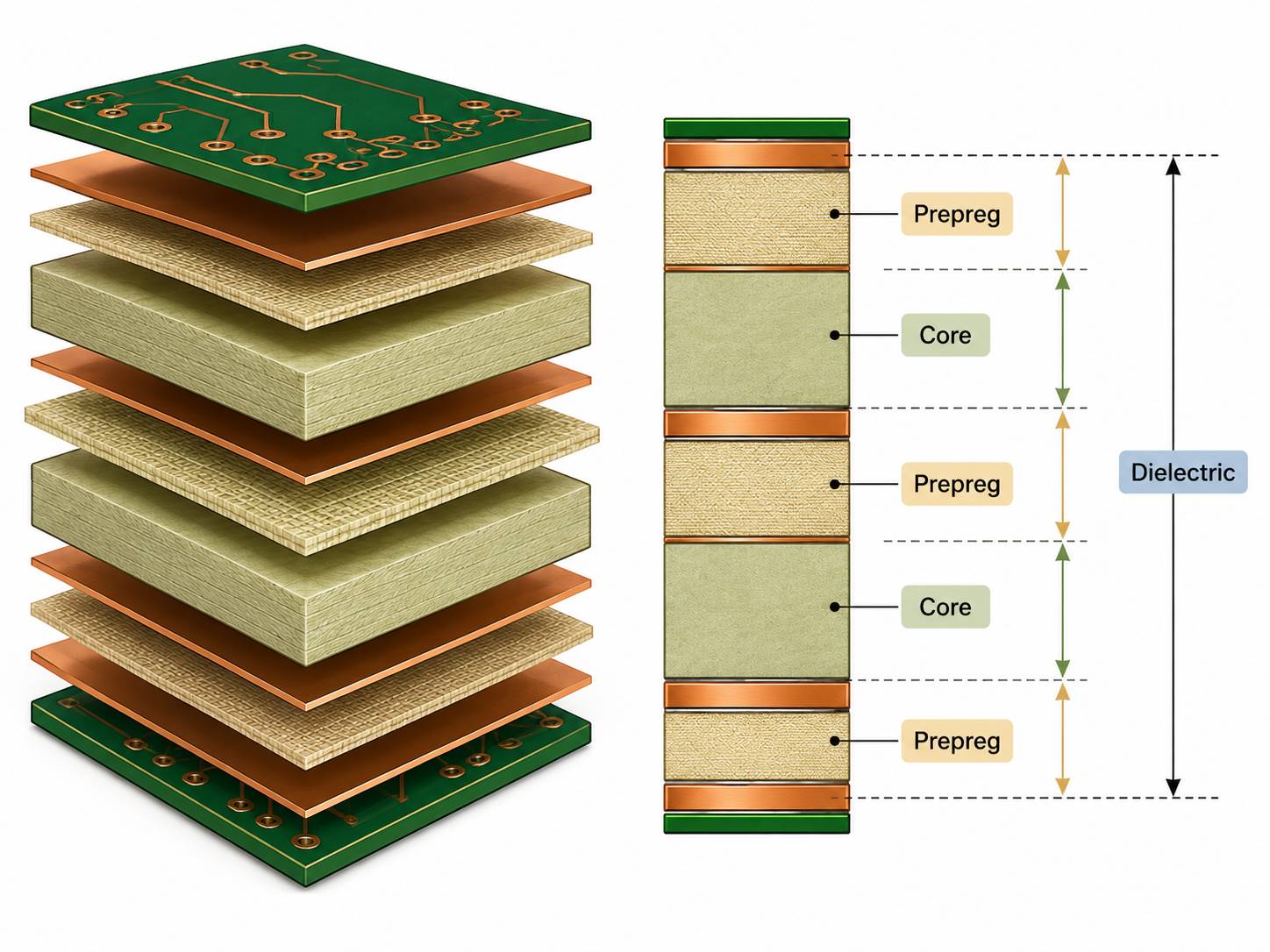
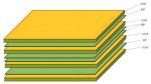
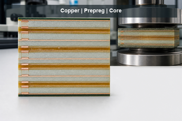
Finished thickness is created by the complete pressed stack, not by one laminate sheet. A 2-layer board may use a copper-clad core and solder mask. A multilayer board combines etched cores, prepreg bonding layers, outer copper, plating and surface coatings. Press temperature, pressure, resin flow and copper distribution affect the result.
- Core thickness: defines much of the rigid dielectric structure and provides copper on one or both sides.
- Prepreg type and count: determine bonding thickness after resin flows into copper features and cures.
- Copper weight: changes the conductor height and the volume of resin needed to fill around traces and planes.
- Layer count: adds copper and dielectric interfaces, increasing the number of variables in the pressed stack.
- Plating and finish: add smaller local thickness contributions, especially on outer copper and hole walls.
- Material system: affects resin content, glass style, pressed thickness, thermal expansion and availability.
Prepreg should not be treated as a fixed spacer before lamination. Its final thickness depends on glass style, resin content, copper pattern density and the press cycle. For controlled builds, the fabricator models the pressed result and selects a balanced set of cores and prepregs. A PCB thickness calculator can support an early estimate, but it cannot replace the production stackup.
How Thick Are 2-, 4-, 6-, 8-, 12- and 32-Layer PCBs?
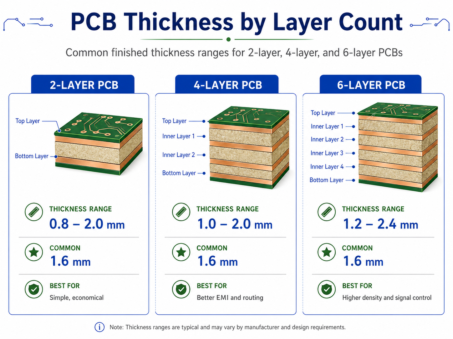
Layer count does not assign one compulsory board thickness. The finished value depends on routing density, copper weight, dielectric spacing, via structure and mechanical requirements. The following ranges are practical starting points for rigid FR4 discussions, not universal standards.
| Layer Count | Common Starting Thicknesses | Important Constraint |
|---|---|---|
| 2 layers | 0.8, 1.0, 1.2 or 1.6 mm | Core thickness usually dominates the construction |
| 4 layers | 1.0, 1.2 or 1.6 mm | Plane spacing and outer copper affect the final build |
| 6 layers | 1.2, 1.6 or 2.0 mm | More dielectric interfaces must fit the impedance plan |
| 8 layers | 1.6, 2.0 or 2.4 mm | Routing density and via aspect ratio become more influential |
| 12 layers | 1.6, 2.0, 2.4 or 3.2 mm | Thin dielectrics or HDI may be needed to limit total thickness |
| 32 layers | Custom multilayer construction | No universal value; lamination, drilling and reliability govern the build |
A 4-layer PCB can be 0.8 mm or 2.0 mm, and a 12-layer PCB can sometimes remain near 1.6 mm by using thin cores and prepregs. That does not mean the thinnest possible build is best. Very thin dielectrics can increase coupling, demand tighter registration and make resin filling more difficult. Very thick builds can increase plated-hole aspect ratio and create longer via stubs.
The layer structure should be selected before the board outline and mechanical system are frozen. The related 4 layer vs 2 layer PCB comparison explains how the extra planes change routing and EMC behavior; thickness remains a separate, coordinated decision.
How Does PCB Thickness Affect Impedance and Signal Integrity?
Total board thickness affects the available stackup space, but controlled impedance is governed by the local transmission-line geometry. Trace width, copper thickness, dielectric thickness, dielectric constant, solder mask and reference-plane relationship determine the impedance of a microstrip or stripline.
Changing a 1.6 mm board to 1.2 mm does not automatically change every trace impedance. If the relevant dielectric spacing and material properties remain the same, some signal layers may retain their geometry. In practice, however, reducing total thickness often forces changes to cores and prepregs, so the impedance model must be recalculated.
Thicker boards can also produce longer through-vias and longer unused via stubs. At higher data rates, those stubs may create resonances and insertion-loss problems. Backdrilling, blind vias or a different layer assignment may be needed. A production impedance control PCB therefore links the trace model to the confirmed laminate construction and measured impedance coupons.
How Does PCB Thickness Affect Mechanical Fit and Connector Compatibility?
Mechanical interfaces often set a harder thickness limit than the electrical circuit. Card-edge connectors specify an acceptable board-thickness range so their contacts apply the intended normal force. Board guides, slots, bezels, standoffs and enclosures also have limited clearance. A nominal change of a few tenths of a millimeter can affect insertion, alignment or screw loading.
- Confirm card-edge connector slot width and contact engagement.
- Check press-fit pin length, compliant-zone position and supported board range.
- Verify standoff height, enclosure gaps and component clearance.
- Review board span, mounting-hole spacing and bending load.
- Include finished-thickness tolerance in the mechanical stack analysis.
Thin boards may need additional support during insertion or handling. Thick boards provide stiffness but increase weight and can move component terminals relative to the enclosure. The mechanical drawing should therefore use the full allowed thickness range, not only the nominal value.
How Does PCB Thickness Influence Warpage, Assembly and Reliability?
Board thickness contributes to bending stiffness, but warpage depends on material modulus, copper balance, stack symmetry, moisture, temperature and panel design. A thin board is more easily deflected by handling, component weight and reflow fixtures. A thick asymmetric board can still warp if copper and dielectric structures are poorly balanced.
During soldering, the PCB experiences a temperature gradient while copper, glass and resin expand at different rates. Large copper areas on one side, uneven component mass or an unbalanced stack can create bow and twist. The board warpage guide explains how stack symmetry, copper distribution, panel support and reflow conditions work together.
Assembly equipment also has practical limits. Very thin boards may require carriers for solder-paste printing, placement and reflow. Very thick boards have greater thermal mass and may need a profile that heats solder joints adequately without overstressing components. Depanelization, connector insertion and functional-test fixtures must use forces that do not bend or crack the finished assembly.
What Is PCB Thickness Tolerance and How Is It Measured?
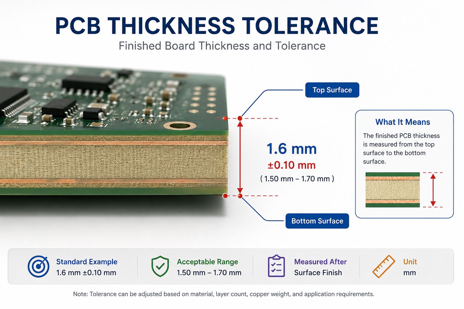
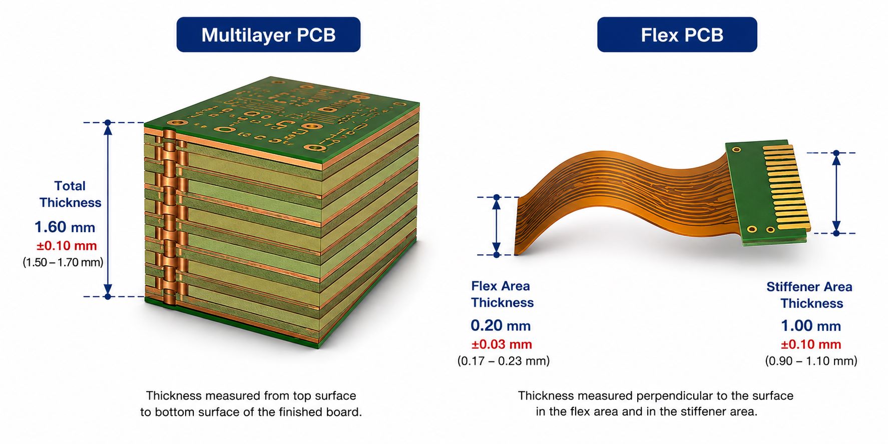
PCB thickness tolerance is the permitted difference between nominal and actual finished thickness. A commercial rigid FR4 build commonly uses a percentage tolerance such as ±10%, but the actual requirement must be confirmed for the material, thickness and construction. A 1.6 mm board with ±10% tolerance has an acceptance range of 1.44-1.76 mm.
Tighter tolerance may be justified for card-edge contacts, press-fit components, controlled mechanical gaps or precision fixtures. It can require a more restricted material set and closer process control. The drawing should state the nominal value, tolerance and whether the measurement includes solder mask when that distinction is mechanically significant.
Finished boards are commonly checked with a calibrated micrometer or thickness gauge. Measurements should be taken at defined locations, away from edge burrs, local copper buildup or surface contamination. Multiple points reveal thickness variation across the panel. Cross-section analysis is used when the individual core, prepreg, copper or plating contributions must be verified rather than only the total board thickness.

When Should You Use a Thin or Thick PCB?
Use a thinner rigid PCB when product height and weight are constrained, the board is mechanically supported and the stackup can still meet impedance, insulation and assembly requirements. Common thin choices include 0.6, 0.8, 1.0 and 1.2 mm. An extra thin PCB needs more attention to handling, panel support, drilling and warpage than a conventional 1.6 mm board.
Use a thicker PCB when the structure needs greater stiffness, the layer stack needs more dielectric space, the board spans a large unsupported area or a connector system requires a specific engagement depth. Common thicker choices include 2.0, 2.4 and 3.2 mm. Thickness alone does not improve current capacity or thermal performance; copper geometry, material properties and the complete heat path still control those functions.
Keep 1.6 mm when it satisfies all electrical and mechanical constraints. It is usually the lowest-risk starting point because materials, assembly fixtures and connector ecosystems are widely compatible with it. Move away from that value only for a defined reason, then validate the linked stackup and mechanical changes.
How Should Finished Thickness Be Defined in PCB Documentation?
Gerber or ODB++ image data defines conductor, mask and legend geometry, but it does not reliably define the required finished board thickness. The value belongs in the fabrication drawing, manufacturing notes or an approved stackup table. The same controlled document should identify the unit and tolerance.
For a simple 2-layer board, a note such as “Finished board thickness: 1.60 mm ±10%” can be sufficient when no special stack construction is required. A controlled-impedance multilayer board needs an approved stackup showing layer order, copper weight, material family, core and prepreg construction, dielectric targets and finished thickness. Mechanically critical designs should also identify connector or press-fit constraints so the allowed range is consistent across drawings.
Revision control matters because changing finished thickness can alter enclosure fit, impedance geometry, via aspect ratio, test fixtures and assembly support. A thickness change should therefore trigger review of the stackup and mechanical interfaces instead of being treated as an isolated fabrication option.
FAQ About Standard Printed Circuit Board Thickness
Is 1.6 mm the only standard PCB thickness?
No. It is the most common rigid FR4 value, but 0.4, 0.6, 0.8, 1.0, 1.2, 2.0, 2.4 and 3.2 mm are also regularly used when the stackup and product mechanics support them.
How thick is a 2-layer PCB board?
A 2-layer rigid PCB is often 1.6 mm, but 0.8, 1.0 and 1.2 mm are common for compact products. The copper-clad core usually contributes most of the finished thickness.
How thick is a 4-layer PCB?
Many 4-layer PCBs use 1.6 mm, while 0.8, 1.0, 1.2 and 2.0 mm are possible. The selected cores and prepregs must provide the required plane spacing and impedance geometry.
Does a 12-layer PCB have to be thicker than 1.6 mm?
No. Some 12-layer constructions can fit within 1.6 mm by using thin dielectrics. Other designs need 2.0, 2.4 or 3.2 mm for routing, isolation, copper or via requirements.
Does thicker PCB material carry more current?
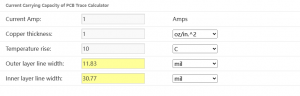
Not by itself. Current capacity depends mainly on copper thickness, trace or plane geometry, allowed temperature rise, airflow and the complete thermal path.
Can a PCB thickness calculator define the production stackup?
A calculator can estimate total thickness, but production values depend on pressed prepreg thickness, copper pattern, material data and lamination behavior. The fabricator’s confirmed stackup is the final reference.
Is solder mask included in finished PCB thickness?
Practices can differ. Solder mask contributes only a small amount, but mechanically critical drawings should state whether the specified finished thickness includes mask and where measurement is taken.
What tolerance is common for a 1.6 mm PCB?
±10% is a common commercial reference, corresponding to 1.44-1.76 mm, but the applicable tolerance depends on the material and construction and must be stated on the drawing.
Conclusion
Standard printed circuit board thickness is commonly 1.6 mm, but that default is only correct when the layer stack, impedance, connector, enclosure, assembly and tolerance requirements agree with it. A sound design separates total board thickness from copper thickness, defines the finished value in controlled documentation and verifies the actual production range.
EBest Circuit (Best Technology) manufactures rigid FR4 boards from very thin 2-layer constructions through thick multilayer builds, subject to material, stackup, dimensions and engineering review. For technical support on a thickness-sensitive PCB design, contact sales@bestpcbs.com.