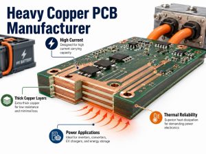
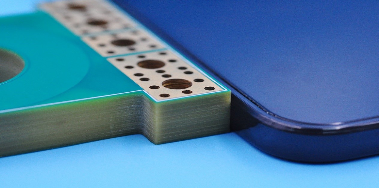
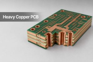
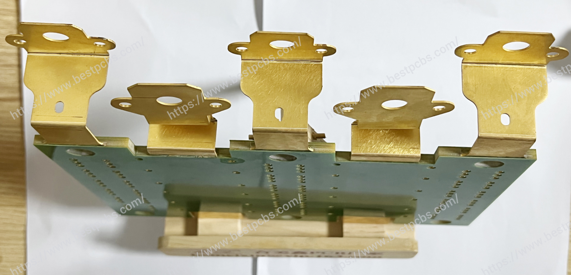
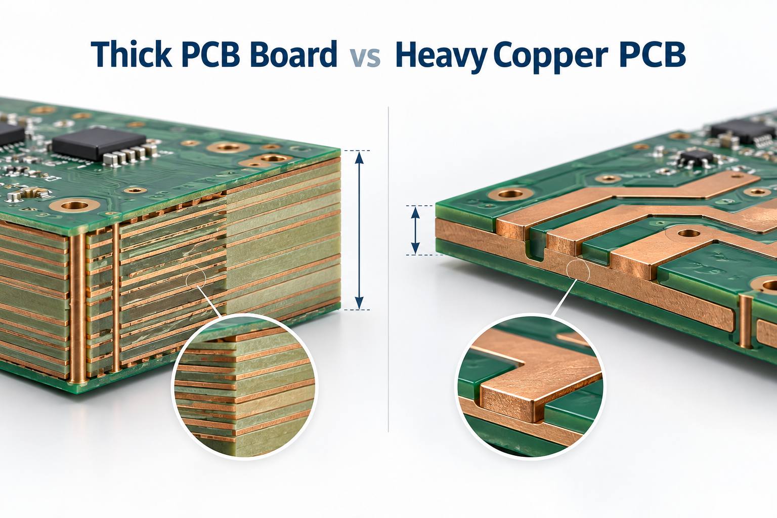
A thick pcb board and a heavy copper PCB solve different engineering problems. The first increases the total finished thickness of the board; the second increases the copper thickness on selected or all conductive layers. A board can be mechanically thick without carrying high current, and a heavy copper design can fit inside a conventional overall thickness.
This distinction affects stackup planning, hole sizes, impedance, thermal behavior, connector fit, manufacturing cost, and the information a fabricator needs before quotation. This guide compares the two constructions so engineers and buyers can specify the right one instead of treating “thick board” and “thick copper” as interchangeable terms.
What Is a Thick PCB Board?
A thick PCB board is a rigid printed circuit board whose total finished thickness is greater than the common construction used for a similar product. The measurement spans the complete board from one outer surface to the other. It includes cores, cured prepregs, copper layers, plating, solder mask, and smaller finish contributions.
The term describes a mechanical dimension, not a specific copper weight. Designers may choose a thicker construction to:
- Increase stiffness across a large unsupported area.
- Support transformers, relays, power modules, large connectors, or other heavy components.
- Meet card-edge, press-fit, guide-rail, enclosure, or mounting requirements.
- Fit additional routing and reference-plane layers into a multilayer stackup.
- Provide required dielectric spacing between conductors.
- Control bending in equipment exposed to vibration or mechanical handling.
A thick board should not be selected only because it appears stronger. Extra thickness can create higher hole aspect ratios, longer routing cycles, different depaneling limits, more material usage, and tighter connector-fit constraints.
How Thick Is a PCB Board?
The practical answer to “how thick is a pcb board” depends on the application and the complete stackup. Many rigid FR-4 boards use a finished thickness near 1.6 mm, while thinner products may use 0.8, 1.0, or 1.2 mm. Mechanically demanding or high-layer-count designs may use 2.0, 2.4, 3.2 mm, or another project-specific value.
These numbers are not automatic manufacturing categories. A 2.4 mm two-layer board with generous holes is usually less demanding than a 2.4 mm multilayer board with small plated holes, controlled impedance, heavy outer copper, and a strict finished-thickness tolerance. The fabricator must review the thickness together with:
- Layer count and copper distribution.
- Core and prepreg constructions.
- Smallest drilled and finished hole sizes.
- Plated-through, blind, buried, or filled via structures.
- Controlled-impedance geometries.
- Board dimensions, panelization, and routing method.
- Connector, press-fit, and enclosure tolerances.
For a broader dimensional reference, see our guide to standard printed circuit board thickness.
What Is the Standard PCB Thickness?
The question “what is the standard pcb thickness” usually refers to 1.6 mm, approximately 0.062 inch. It is a widely used rigid-board value because common laminate constructions, connectors, housings, fixtures, and assembly processes are often designed around it. However, 1.6 mm is a common default rather than a universal rule.
Finished thickness is built from real laminate and prepreg options. Prepreg does not behave like a fixed spacer: its pressed thickness changes with glass style, resin content, copper pattern density, resin flow, and the lamination cycle. Material suppliers such as Isola publish laminate and prepreg construction data that fabricators use when developing manufacturable stackups.
If a mechanical drawing calls out only an unusual finished thickness but does not define the stackup, the designer should let the PCB manufacturer propose available core and prepreg combinations. This is safer than forcing a theoretical build that depends on unavailable materials or unrealistic pressed thicknesses.
Thick PCB Board vs Heavy Copper PCB: What Is the Difference?
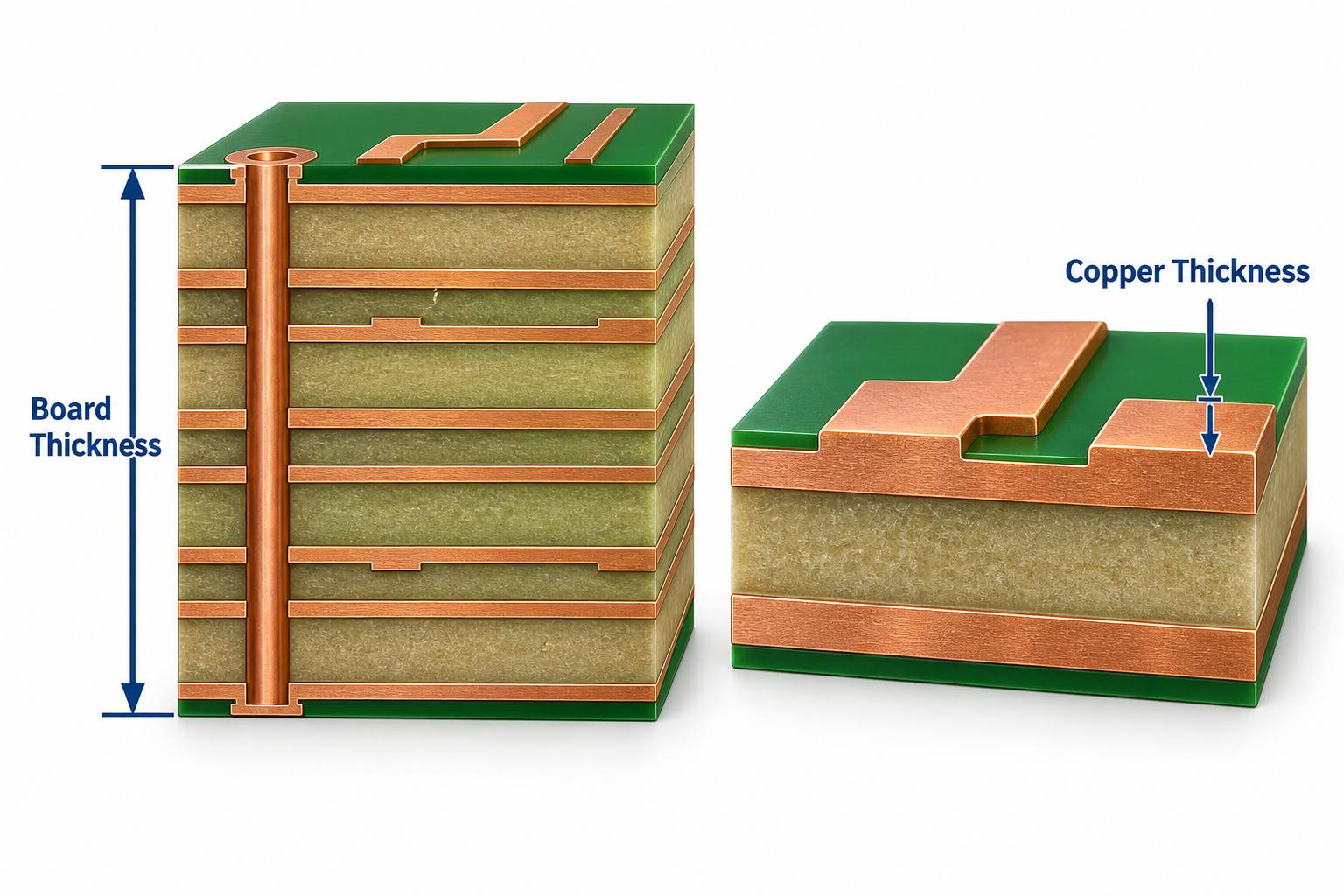
The shortest distinction is simple: board thickness is a mechanical stack dimension, while copper thickness is a conductor dimension. They influence different parts of PCB performance and manufacturing.
| Comparison | Thick PCB Board | Heavy Copper PCB |
| Primary definition | Greater total finished board thickness | Greater copper thickness or copper weight on one or more layers |
| Main purpose | Mechanical stiffness, stackup space, connector fit, or dielectric spacing | High-current conduction, lower conductor resistance, heat spreading, or robust power connections |
| Most affected design data | Stackup, hole size, aspect ratio, impedance, enclosure, routing, and tolerance | Trace width and spacing, pad geometry, etching, resin fill, plating, current rise, and thermal path |
| Typical manufacturing concern | Deep drilling, hole preparation, plating coverage, lamination, routing, and warpage control | Etch compensation, copper balance, resin filling around tall conductors, conductor definition, and thermal mass |
| Can it exist without the other? | Yes. A thick board can use standard copper. | Yes. A heavy copper board can retain a conventional finished thickness. |
For example, a 3.2 mm FR-4 board with 1 oz copper is mechanically thick but is not a heavy copper PCB. A 1.6 mm board with 4 oz copper is a heavy copper design even though its total thickness is conventional. Some power products need both: a thick structure for stiffness and thick copper for electrical and thermal performance.
How Does a Thick Board Change Stackup and Impedance?
Increasing total board thickness changes the dielectric distance available between copper layers. If trace width, copper thickness, and dielectric properties remain unchanged, a larger trace-to-reference-plane distance changes characteristic impedance. Therefore, a designer cannot simply stretch every dielectric layer to reach a new finished thickness and expect the same controlled-impedance result.
A practical thick-board stackup review covers:
- Reference-plane location: High-speed signals still need a nearby and continuous return plane.
- Dielectric selection: Core and prepreg choices must match available material constructions and the required pressed thickness.
- Copper balance: Symmetric copper and dielectric distribution helps reduce lamination stress and bow or twist.
- Resin filling: Heavy copper or uneven pattern density may require higher-resin prepreg to fill around conductors.
- Finished tolerance: The stackup must leave a realistic process window for material and lamination variation.
Do not approve the mechanical thickness independently from impedance. Send the impedance table, target values, referenced layers, and any material restrictions with the stackup so the fabricator can model the construction as one system.
How Do Drilling and Plating Limits Change?
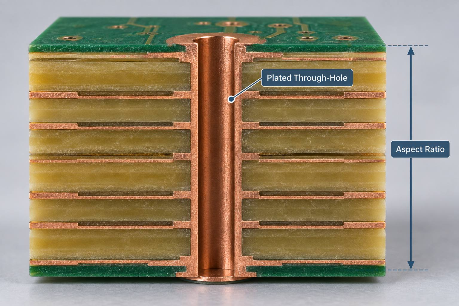
As a board becomes thicker, a mechanically drilled hole becomes deeper. If the drill diameter stays small, the hole aspect ratio rises. This makes debris removal, desmear, activation, and copper deposition inside the barrel more demanding. The result can be thin plating in the center of the hole, barrel voids, poor registration margin, or lower thermal-cycling reliability.
Aspect ratio is commonly expressed as board thickness divided by drilled hole diameter. It is a DFM relationship, not a target that should be pushed without considering the material, layer count, plating process, copper requirement, and acceptance class. A thicker finished board may need one or more of the following changes:
- Increase the mechanically drilled hole diameter.
- Use staged or controlled drilling conditions.
- Adjust the via structure instead of using one deep through-hole.
- Increase annular-ring and registration allowance where required.
- Specify hole-wall copper and microsection acceptance clearly.
- Review press-fit hole tolerances and final plating buildup.
IPC-6012F establishes qualification and performance requirements for rigid printed boards, including multilayer constructions with plated-through, blind, buried, and microvia structures. The applicable class, customer drawing, procurement specification, and agreed deviations should be defined before production.
Heavy Copper PCB Design: What Must Be Reviewed?
Heavy copper PCB design starts with electrical and thermal requirements, not with a higher copper weight chosen by habit. A thicker conductor can reduce resistance and support more current, but the result also depends on trace width, conductor location, ambient conditions, allowed temperature rise, adjacent copper, airflow, duty cycle, terminal design, and heat-transfer paths.
IPC-2152 provides guidance on the relationship between current, conductor dimensions, and acceptable temperature rise. It is a better basis for conductor sizing than assuming that a mechanically thicker board will automatically carry more current.
Manufacturing review should include:
- Copper weight required on every inner and outer layer.
- Minimum line width and spacing after etch compensation.
- Pad, via, and neck-down geometry at high-current transitions.
- Resin filling around tall copper features.
- Copper balance across the panel and stackup.
- Thermal reliefs, solderability, and assembly heat demand.
- Finished copper and plated-hole copper acceptance.
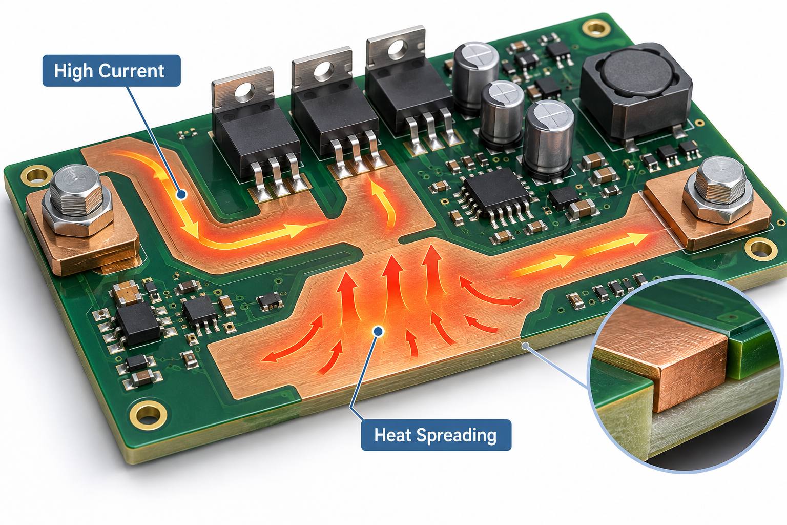
EBest Circuit supports heavy copper PCB projects for power distribution, heat spreading, planar transformers, power converters, and related high-current applications. Exact copper, spacing, stackup, and test requirements must be confirmed against the production data.
Which Construction Should You Choose?
Choose the construction from the problem you are trying to solve. Mechanical stiffness does not replace electrical conductor sizing, and additional copper does not guarantee connector fit or board rigidity.
| Primary Requirement | Review First | Likely Direction |
| Large board or heavy components need more rigidity | Board dimensions, mounting points, vibration, and enclosure support | Thicker finished board |
| High current with an acceptable temperature rise | Current, trace width, copper weight, duty cycle, and cooling | Heavy copper PCB |
| More routing and reference planes | Layer count, impedance, dielectric spacing, and via structure | Thicker multilayer stackup, if required |
| High current plus mechanical stiffness | All electrical, thermal, stackup, drilling, and enclosure constraints | Combined thick-board and heavy-copper construction |
| Connector or card-edge fit | Specified finished thickness and tolerance at the mating interface | Board thickness driven by connector geometry |
If the design needs both thickness and heavy copper, review them together before layout release. Thick copper consumes vertical space, changes resin demand, restricts fine features, and can alter the final thickness. A late copper-weight change can therefore invalidate the stackup and controlled-impedance calculations.
What Should You Send for a Manufacturing Review?
A useful DFM package lets the fabricator evaluate the mechanical and conductor requirements separately, then confirm how they interact. Include:
- Gerber or ODB++ fabrication data and drill files.
- Layer count and proposed stackup.
- Target finished board thickness and tolerance.
- Base material, Tg, CTI, thermal, or high-frequency requirements.
- Copper weight for every layer and any selective heavy-copper areas.
- Smallest drilled hole, smallest finished hole, via types, and filled-via requirements.
- Controlled-impedance values and referenced layer pairs.
- Board dimensions, panel or delivery format, outline tolerance, and connector requirements.
- Surface finish, solder mask, legend, electrical test, acceptance class, and required reports.
- Prototype and production quantities plus the required delivery date.
If the project is already defined as a thick mechanical build, our thick PCB board manufacturing guide explains the detailed stackup and quotation review path.
FAQ About Thick PCB Boards and Heavy Copper PCBs
Is a 2.0 mm PCB considered thick?
It is thicker than the common 1.6 mm construction, but whether it needs special processing depends on its layer count, material, dimensions, holes, copper weight, tolerances, and routing method.
Does a thick PCB carry more current?
Not automatically. Current capacity is primarily determined by conductor geometry, temperature-rise limits, copper environment, cooling, and operating conditions. Overall board thickness is a separate mechanical property.
Can a heavy copper PCB be only 1.6 mm thick?
Yes. A fabricator may build heavy copper into a conventional finished thickness if the layer structure, dielectric spacing, resin fill, feature sizes, and tolerance can be manufactured reliably.
Why are small vias difficult in a thick board?
The deeper hole creates a higher aspect ratio. Hole cleaning and uniform copper deposition become more demanding, especially when the finished hole is small or the specified barrel copper is high.
Should I specify copper in ounces or micrometers?
Either can be used if the procurement documents are consistent, but clearly distinguish base copper from finished copper after plating. State the requirement for each layer rather than using one value for the entire PCB.
Can board thickness be changed after impedance routing is complete?
Only after the impedance geometry is recalculated. Changing the dielectric distance to the reference plane can change impedance, so the fabricator must review the revised stackup, trace width, spacing, copper thickness, and material properties.
How Can EBest Circuit Support Your PCB Project?
EBest Circuit reviews thick-board and heavy-copper requirements as two connected but distinct engineering inputs.
Send your Gerber or ODB++ data, stackup, finished thickness, copper weight by layer, drill table, impedance requirements, material notes, surface finish, test standard, quantity, and delivery target to sales@bestpcbs.com. We will review the manufacturable construction before quotation and prototype release.