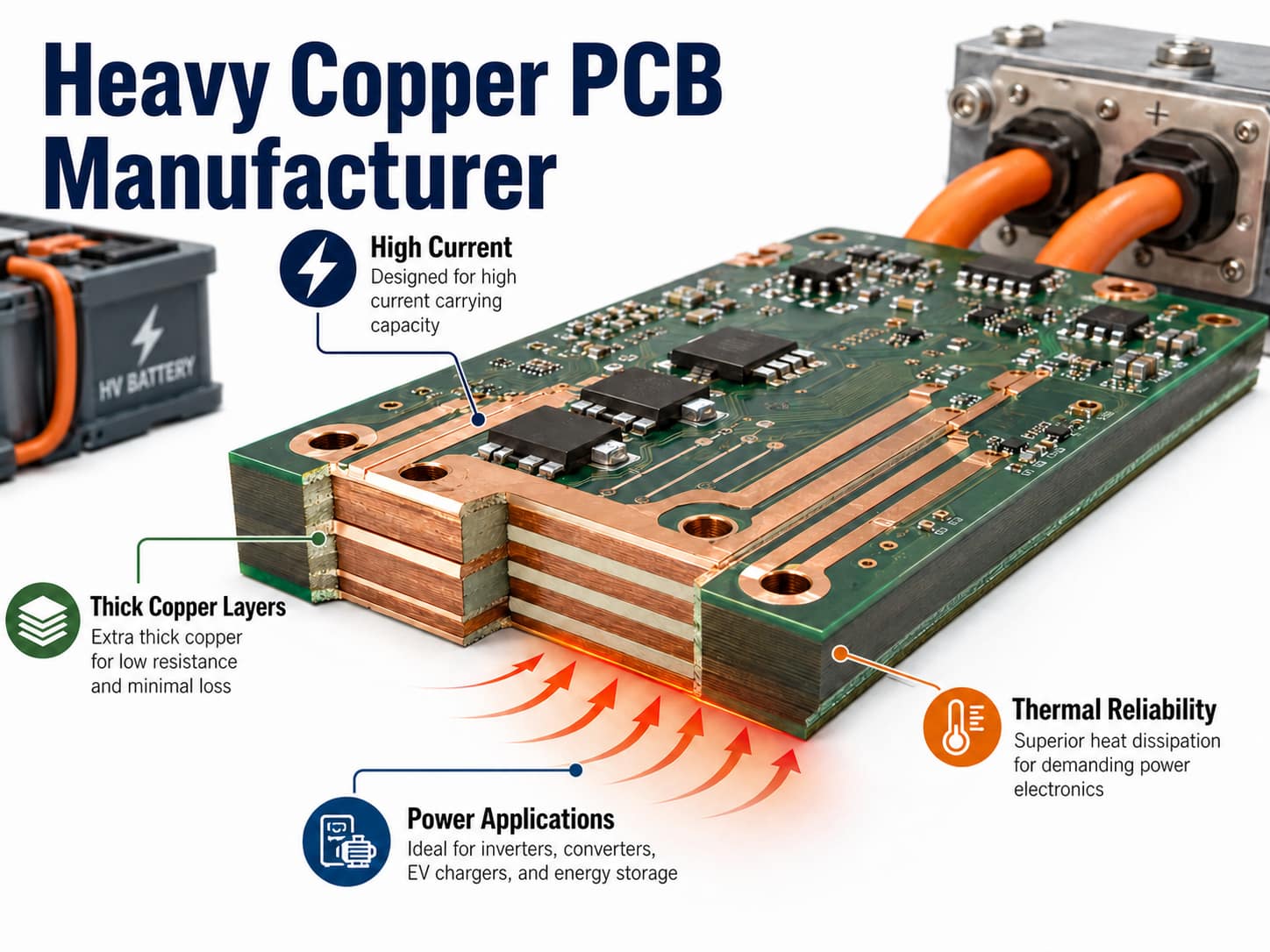
A heavy copper PCB manufacturer builds boards for applications that require higher current capacity, improved heat dissipation, and stronger mechanical reliability than standard copper PCB constructions. By increasing copper thickness on inner or outer layers, these PCBs can support high-power circuits used in battery systems, power converters, industrial equipment, EV charging systems, renewable energy controls, and other demanding electrical applications.
EBest Circuit provides custom heavy copper PCB manufacturing with support for thick copper layers, mixed copper stack-ups, high-current designs, and complex multilayer structures. Our engineering team reviews copper thickness, layer configuration, thermal requirements, via structures, and manufacturing feasibility before production to help customers develop reliable power PCB solutions. Send your Gerber files, stack-up requirements, or application details to sales@bestpcbs.com for engineering review and quotation.
What Maximum Copper Thickness Can Be Achieved for Heavy Copper PCBs?
The maximum copper thickness of a heavy copper PCB depends on the layer position, board size, copper distribution, etching requirements, and manufacturing process capability. Unlike standard PCBs using 1 oz or 2 oz copper, heavy copper designs require specialized processing to maintain copper thickness consistency and reliable circuit formation.
EBest Circuit supports the following verified standard and special-project copper ranges. PCB copper weight must be evaluated with board size, copper distribution, spacing, dielectric fill, and process requirements.
| Copper Location | Typical Thickness Capability |
| Inner layer copper | Standard 0.5–5 oz; special projects 5–20 oz |
| Outer layer copper | Standard 1–5 oz; special projects 5–20 oz |
| Mixed copper designs | Available after stack-up and DFM review |
| 100 oz+ request | Project-specific engineering review; not a standard capability |
For 100 oz+ copper PCB designs, additional engineering evaluation is required because extremely thick copper affects:
- Trace geometry and etching compensation
- Copper distribution balance
- Lamination pressure and resin filling
- Thermal stress during manufacturing
- Finished board weight and mechanical strength
Heavy copper capability is not only determined by copper thickness. A reliable manufacturing process must also maintain proper layer alignment, insulation spacing, and plated hole quality.
What Heavy Copper PCB Stack-Up Configurations Are Available?
Heavy copper PCBs can be manufactured with different stack-up structures depending on current requirements, thermal performance, signal requirements, and cost targets.
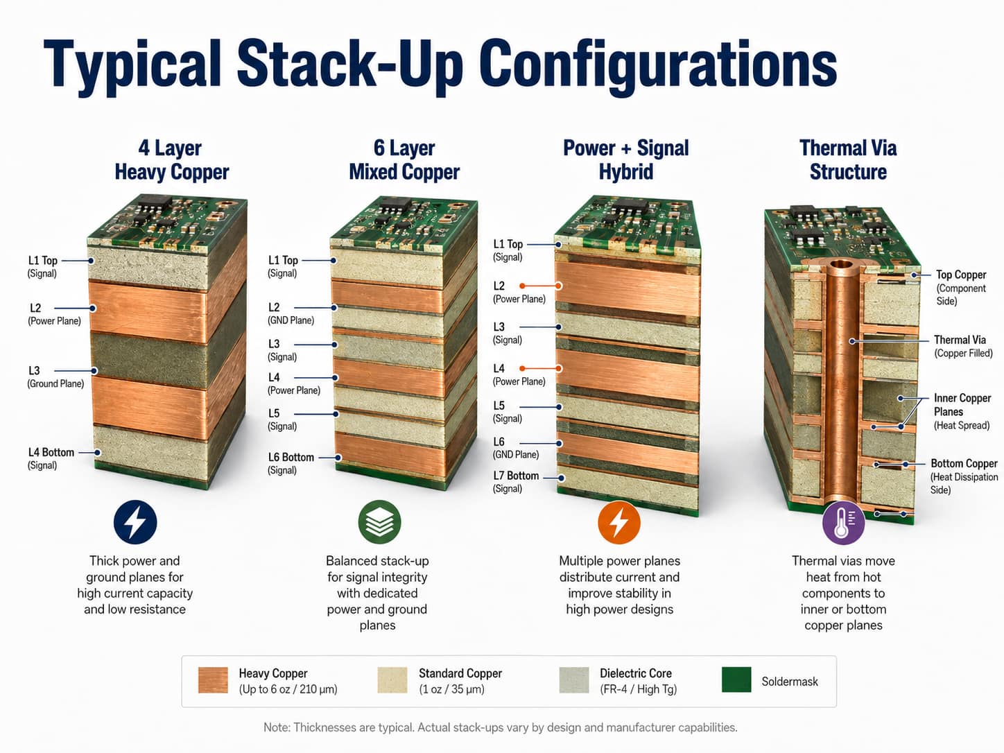
Typical configurations include:
| Stack-Up Type | Typical Application |
| 4-layer heavy copper PCB | Power control boards, industrial electronics |
| 6-layer mixed copper PCB | Power and signal integration |
| Heavy copper outer layers with standard inner layers | High current connection areas |
| Heavy copper power layers with thermal vias | Heat-sensitive applications |
A high current PCB stackup often combines heavy copper layers with standard signal layers. This approach allows engineers to increase current capacity in specific areas without unnecessarily increasing the cost and weight of the entire PCB.
A typical multilayer structure may include:
- Thick copper power planes for current distribution
- Standard copper signal layers for control circuits
- Dedicated thermal layers for heat spreading
- Controlled impedance layers when high-speed signals are required
The final stack-up should be reviewed during the engineering stage to ensure copper thickness, dielectric thickness, and manufacturing capability are properly matched.
Which Materials and Prepreg Systems Are Used for Heavy Copper PCBs?
Heavy copper PCB materials must provide sufficient mechanical strength, thermal stability, and reliable insulation performance under high current operation.
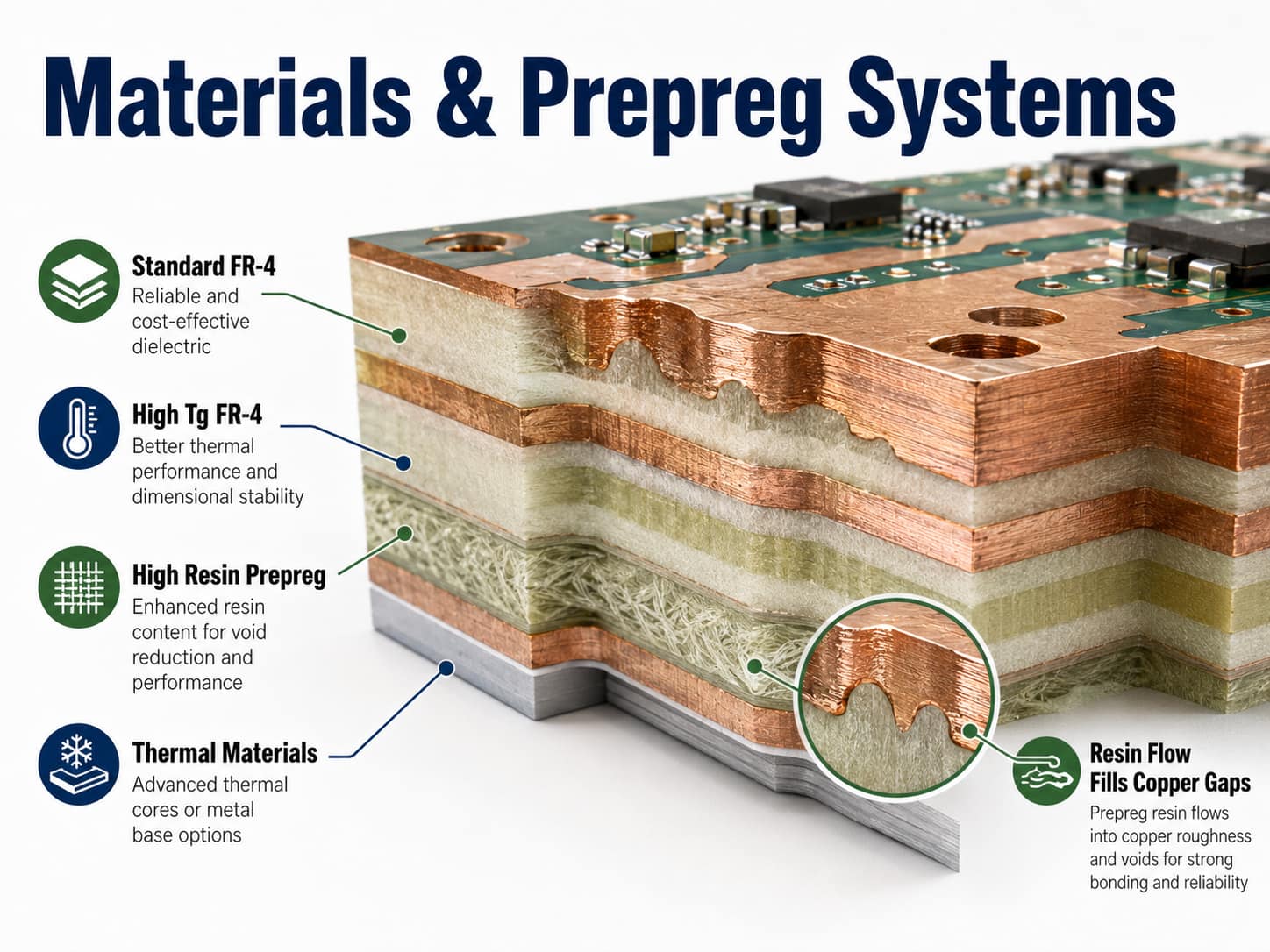
Common material options include:
| Material System | Application Advantage |
| Standard FR-4 | General heavy copper applications |
| High Tg FR-4 | Higher thermal reliability |
| Thermal management materials | Improved heat dissipation |
| High resin content prepreg | Better copper gap filling |
Prepreg selection is especially important for heavy copper multilayer boards. Thick copper creates larger height differences between copper areas, requiring sufficient resin flow during lamination to prevent voids and ensure reliable insulation.
Material selection depends on:
- Operating temperature
- Current load
- Thermal cycling requirements
- Mechanical environment
- Industry requirements
For high-power applications, engineers should consider both copper thickness and laminate performance rather than focusing only on copper weight.
What Surface Finish Options Are Available for Heavy Copper PCBs?
Surface finish selection depends on component requirements, assembly process, reliability expectations, and storage conditions.
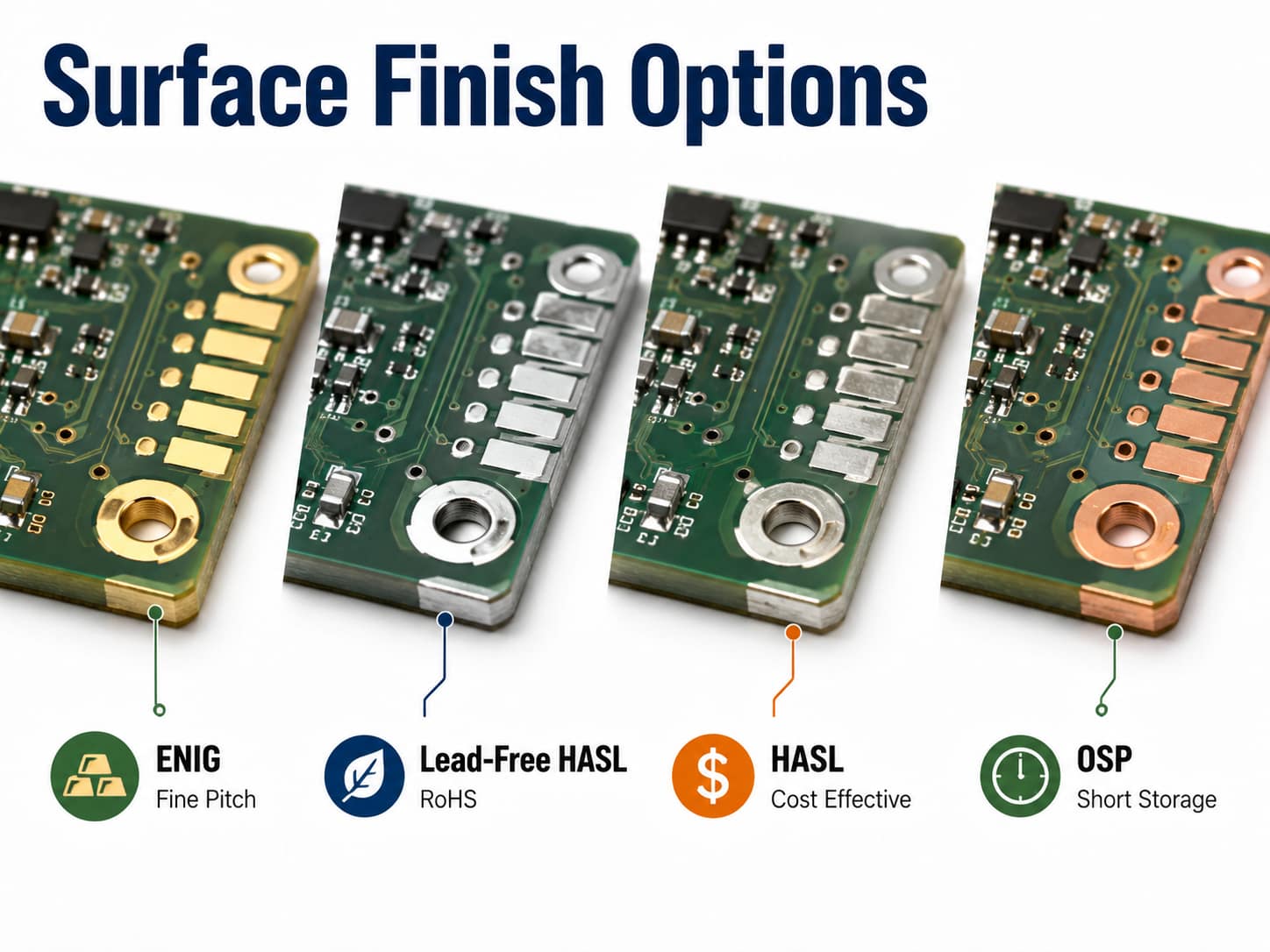
Common surface finishes for heavy copper PCBs include:
| Surface Finish | Typical Application |
| ENIG | Fine-pitch components and high reliability applications |
| Lead-free HASL | Cost-effective industrial applications |
| HASL | Traditional soldering applications |
| OSP | Short-term storage and standard assembly |
For high-current PCBs, surface finish selection should also consider:
- Contact reliability
- Solder joint performance
- Assembly temperature profile
- Long-term environmental exposure
The correct surface finish helps maintain reliable electrical connections throughout the product lifecycle.
What Are the Design Rules and Manufacturing Tolerances for Heavy Copper PCBs?
Heavy copper PCB design requires additional attention compared with standard PCB manufacturing because thicker copper changes trace geometry, spacing requirements, and fabrication conditions.
Important design considerations include:
| Design Factor | Engineering Consideration |
| Trace width and spacing | Requires copper thickness compensation |
| Copper distribution | Avoid excessive imbalance between layers |
| Clearance | Must consider thicker copper profiles |
| Impedance control | Requires stack-up-based calculation |
| Thermal design | Optimize copper planes and heat paths |
During DFM review, engineers typically evaluate:
- Copper thickness versus minimum trace width
- Etching capability
- Layer-to-layer registration
- Resin filling conditions
- Finished board thickness
These high current PCB design guidelines should be confirmed against the proposed copper weight and stack-up during an engineering DFM review. Early communication helps avoid unnecessary redesign during manufacturing.
Which Via Technologies Are Available for Heavy Copper PCB Manufacturing?
Via structures play an important role in heavy copper PCB performance because they influence current flow, thermal transfer, and mechanical reliability.
Available via technologies include:
- Through-hole vias
- Plated through vias
- Thermal via arrays
- Large diameter vias
- Multiple parallel vias for current distribution
For power applications, engineers often use multiple thermal vias under heat-generating components or create parallel via paths to reduce electrical resistance.
Via design should consider:
- Current requirements
- Component heat generation
- Copper thickness
- Assembly conditions
A proper via structure improves both electrical performance and thermal management.
Which Standards and Certifications Apply to Heavy Copper PCBs?
Heavy copper PCB manufacturing for industrial, automotive, medical, and aerospace applications often requires compliance with recognized quality standards.
EBest Circuit supports manufacturing processes aligned with:
| Standard / Certification | Application |
| IPC-6012 | Qualification and performance specification for rigid PCBs |
| IPC-A-600 | PCB acceptance criteria |
| ISO 9001 | Quality management system |
| ISO 13485 | Medical device applications |
| IATF 16949 | Automotive applications |
| AS9100D | Aerospace applications |
Specific requirements depend on the final application, customer specifications, and industry regulations.
Quality control processes may include:
- Electrical testing
- AOI inspection
- X-ray inspection when required
- Dimensional inspection
- Copper thickness verification
What Is the Typical Lead Time for Heavy Copper PCB Production?
Heavy copper PCB lead time depends on copper thickness, layer count, board complexity, testing requirements, and production volume. Review our PCB lead-time guidance as a planning reference; the quotation confirms the actual schedule.
Typical production stages include:
| Production Stage | Time Consideration |
| Engineering review | Based on design complexity |
| Prototype production | Depends on copper thickness and stack-up |
| Volume production | Based on quantity and process requirements |
Compared with standard PCB production, heavy copper boards may require additional process controls, including:
- Special lamination conditions
- Copper thickness verification
- Additional inspection steps
- Manufacturing feasibility review
Providing complete design information during quotation helps shorten engineering evaluation time.
Recommended information includes:
- Gerber files
- Layer stack-up
- Copper thickness requirements
- Current load requirements
- Application environment
What Design Guidelines Should Be Followed for 100 oz+ Heavy Copper PCBs?
100 oz+ heavy copper PCB requests require project-specific feasibility review because extremely thick copper affects electrical performance, manufacturing processes, and mechanical characteristics. This section provides design inputs for evaluation and does not state an unconditional production capability.
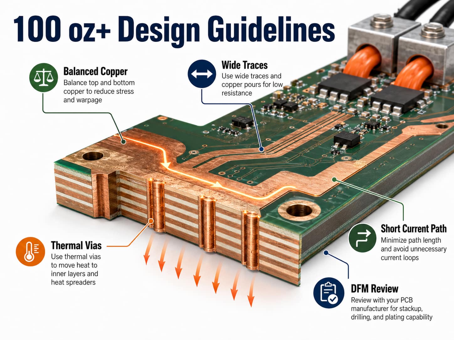
Key design guidelines include:
Optimize copper distribution
Large differences in copper area between layers can create lamination challenges and affect board flatness. Balanced copper distribution improves manufacturing stability.
Consider current path design
High-current paths should use:
- Wider copper areas
- Shorter current routes
- Multiple copper layers when required
- Optimized connection points
Plan thermal management early
High-power applications should consider:
- Large copper planes
- Thermal vias
- Heat spreading structures
- Component placement strategy
Complete DFM review before production
For 100 oz+ designs, customers should provide:
- Maximum current requirement
- Operating temperature
- Mechanical dimensions
- Layer stack-up preference
- Reliability requirements
Early engineering review helps confirm whether the design is suitable for production.
Why Choose EBest Circuit for Heavy Copper PCB Manufacturing?
Selecting a heavy copper PCB supplier requires more than checking the maximum copper thickness. Manufacturing experience, engineering support, and process control directly affect final PCB reliability.
EBest Circuit provides:
- Heavy copper PCB manufacturing capability
- Custom multilayer PCB solutions
- Mixed copper stack-up support
- Engineering DFM review
- Prototype and production support
- PCB assembly integration capability
With more than 20 years of PCB manufacturing experience, EBest Circuit supports customers from initial design evaluation through PCB production and PCBA assembly.
For heavy copper PCB projects, contact sales@bestpcbs.com with your Gerber files, copper requirements, or application details.
Frequently Asked Questions About Heavy Copper PCBs
What copper thickness is considered a heavy copper PCB?
Heavy copper PCBs generally refer to boards using copper thickness above standard PCB levels, commonly starting from 3 oz copper and extending to much higher copper weights depending on the application.
Can you manufacture 100 oz copper PCB?
100 oz+ copper PCB requests require project-specific engineering review. Feasibility can be confirmed only after board size, layer structure, copper distribution, insulation, drilling, plating, and reliability requirements are evaluated.
What applications use heavy copper PCBs?
Heavy copper PCBs are commonly used in power supplies, battery systems, EV equipment, industrial controls, renewable energy systems, and high-current electronics.
What materials are recommended for heavy copper PCBs?
High Tg FR-4, suitable prepreg systems, and thermal management materials are commonly selected based on operating temperature and reliability requirements.
Can heavy copper PCBs include controlled impedance designs?
Yes. Controlled impedance can be considered when heavy copper layers are combined with appropriate dielectric thickness and stack-up planning.
What files are needed for heavy copper PCB quotation?
Customers should provide Gerber files, layer stack-up information, copper thickness requirements, board dimensions, quantity, and application details.
Request a Heavy Copper PCB Manufacturing Review
Whether you need a standard heavy copper PCB or want feasibility feedback on a 100 oz+ high-current concept, EBest Circuit can review your design requirements and provide manufacturing recommendations.
Send your PCB files or technical requirements to sales@bestpcbs.com for engineering evaluation and quotation.
You may also like





Tags: heavy copper pcb design, Heavy copper PCB manufacturer, High Current PCB Design Guidelines, high current pcb stackup, PCB Copper Weight