





Learning how to make labels in KiCad helps you name nets clearly, control signal scope, and prepare readable schematics for PCB layout.
Readers often ask: How do labels work in KiCad? The sections below also show how to create a net label in KiCad, how to add labels in KiCad, and how to use labels in KiCad across single-sheet and hierarchical designs.
Labels make KiCad schematics easier to read and maintain. Instead of drawing a long wire across a page, you can attach matching labels to separate wire segments. KiCad then treats those segments as the same electrical net when the label type and scope allow it.
The main challenge for beginners is choosing the correct label. A local label works only within one schematic sheet. A global label can connect matching nets throughout the project. A hierarchical label connects a child sheet to its parent through a matching sheet pin. KiCad also provides bus labels, directive labels, power symbols, schematic text, and PCB text.
Some of these objects create electrical connectivity. Others are only visual annotations. This guide explains the difference and shows how to place each type correctly.
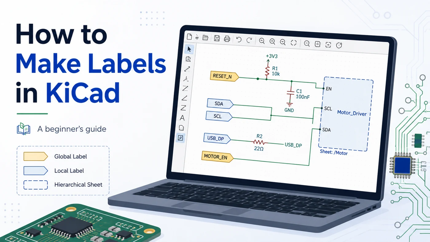
What Are Labels in KiCad?
In the Schematic Editor, an electrical connection is called a net. A net may include symbol pins, wires, junctions, and labels. A label gives the net a meaningful name, such as:
SDASCLRESET_NUSB_DPMOTOR_EN+12V_SENSE
Matching labels can replace long wires, reduce crossings, and make signal names visible during PCB routing.
| Label or text type | Creates connectivity? | Scope | Typical use |
|---|---|---|---|
| Local label | Yes | Current sheet | Same-page signal connections |
| Global label | Yes | Entire project | Shared signals across sheets |
| Hierarchical label | Yes | Parent-child sheet interface | Modular multi-sheet design |
| Bus label | Yes | Bus members | Data, address, or grouped signals |
| Directive label | Assigns rules | Attached net, bus, or area | Net-class and design-rule assignment |
| Power symbol | Yes | Entire project | GND, VCC, +3V3, and power rails |
| Schematic text | No | Visual only | Notes and section headings |
| PCB text | No | Selected board layer | Silkscreen and fabrication markings |
The practical rule is simple: choose a label according to how far the connection should reach.
How to Make a Local Label in KiCad?
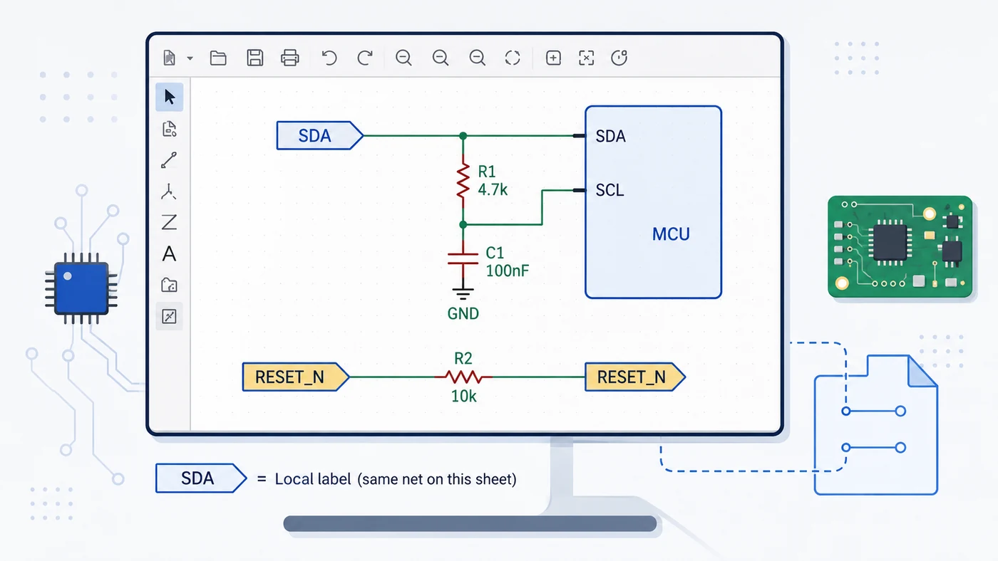
A local label connects matching net names only within the current schematic sheet. It is the best default for signals that do not need to leave that page.
Step-by-Step Instructions
- Open the project and enter the Schematic Editor.
- Draw a short wire from the pin or component connection.
- Press L to open the local label tool.
- Enter the net name, such as
RESET_N. - Adjust the orientation or text size when needed.
- Click OK.
- Move the label until its connection point snaps to the wire endpoint.
- Click to place it.
- Place the same local label on the other wire segment that should connect.
The label’s small square is its electrical attachment point. If the square remains visible beside the wire, the label may not be connected.
Use local labels for:
- SPI or I2C signals contained on one page
- Feedback and enable signals
- Analog measurement nodes
- Same-sheet test points
- Connections that should not reach another sheet
Local labels reduce visual clutter without creating unnecessary project-wide connections.
How to Make a Global Label in KiCad?
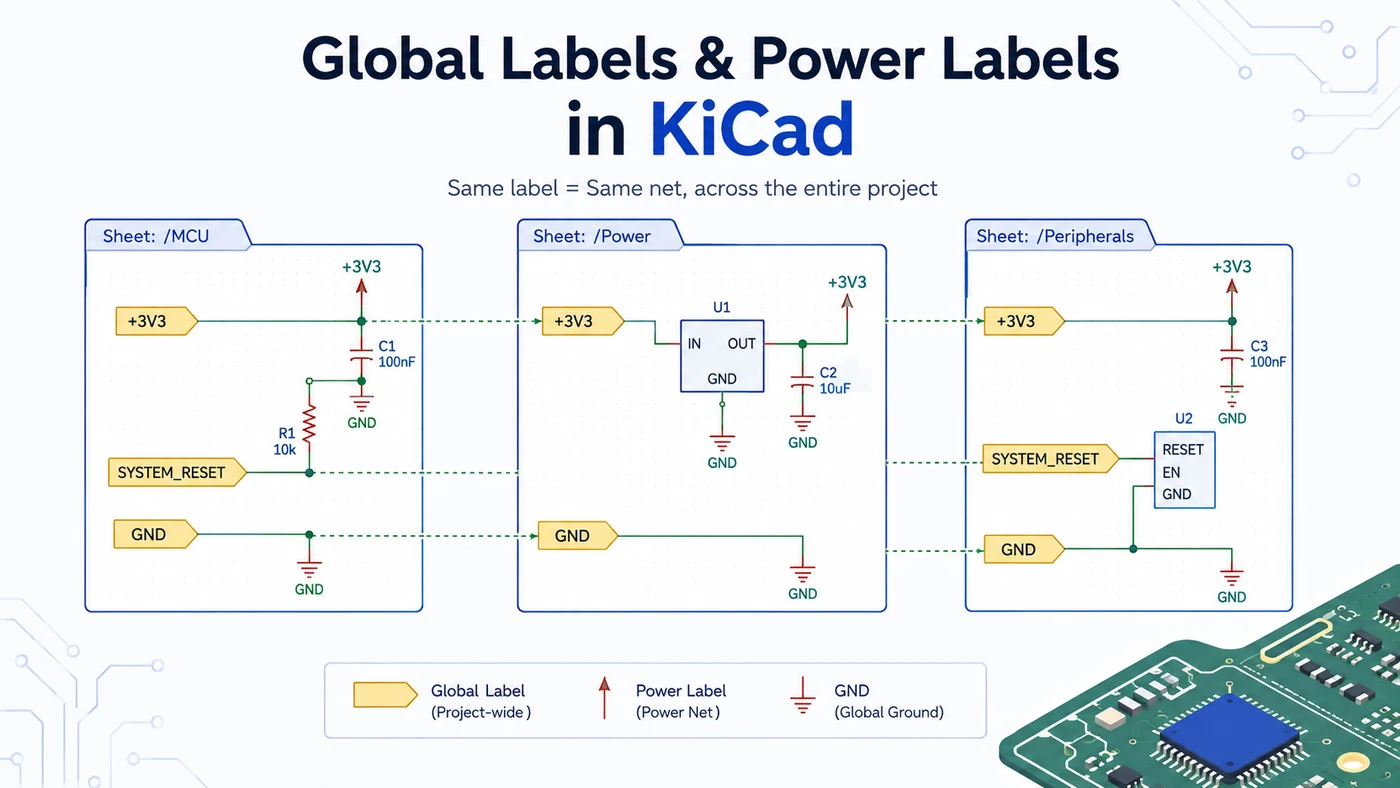
A global label connects every matching global label throughout the schematic project, including labels on different sheets.
Step-by-Step Instructions
- Draw a short wire from the required pin.
- Press Ctrl + L.
- Enter the global label name, such as
SYSTEM_RESET. - Select an orientation and graphical shape.
- Click OK.
- Attach the connection point to the wire.
- Open another sheet and place a global label with exactly the same name.
The input, output, bidirectional, tri-state, and passive shapes describe the intended signal direction visually. They do not change the electrical behavior of the net.
Global labels are suitable for:
- System reset signals
- Shared clocks
- Interrupt lines
- Board-wide enable signals
- Cross-sheet communication nets
- Rails or signals that genuinely apply throughout the project
Do not use global labels simply because they are convenient. Too many global nets can hide signal flow and make accidental connections harder to find. For structured multi-sheet projects, hierarchical labels often provide a clearer interface.
How to Make Hierarchical Labels in KiCad?
Hierarchical labels connect a child schematic sheet to its parent sheet. They are useful when the design is divided into functional modules, such as power supply, sensor, communication, or motor-control blocks.
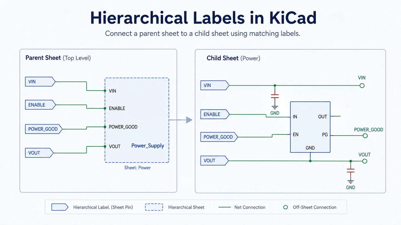
A hierarchical connection requires two matching objects:
- A hierarchical label inside the child sheet
- A sheet pin on the child sheet symbol in the parent sheet
Step 1: Create a Hierarchical Sheet
- Open the parent sheet.
- Press S or choose Place Hierarchical Sheet.
- Draw the sheet symbol.
- Enter a sheet name, such as
Power_Supply. - Enter or select the child schematic filename.
- Confirm the sheet properties.
- Open the new child sheet.
Step 2: Add Hierarchical Labels
- Draw a wire from a signal that must leave the child sheet.
- Press H.
- Enter a name such as
POWER_GOOD. - Select the label shape and orientation.
- Place the label on the wire.
- Repeat for every input, output, or shared connection.
Typical child-sheet labels may include:
VINENABLEPOWER_GOODVOUTFAULT_N
Step 3: Add Matching Sheet Pins
- Return to the parent sheet.
- Select Place Sheet Pins.
- Click the hierarchical sheet symbol.
- Choose the unmatched child-sheet label offered by KiCad.
- Place the sheet pin on the sheet-symbol border.
- Connect the pin to the parent circuit.
The names must match exactly. KiCad’s Sync Sheet Pins tool can identify missing or inconsistent sheet pins and hierarchical labels.
Hierarchical labels are preferable when you want the schematic architecture to remain visible. A reviewer can see which signals enter and leave each functional block without searching for project-wide global names.
How to Make Bus Labels in KiCad?
A bus groups several related nets into one graphical path. Buses are useful for memory, data, address, and multi-channel interfaces.
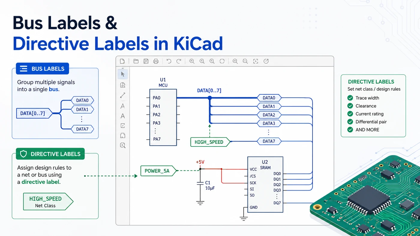
KiCad supports vector buses and group buses.
Vector Bus
A vector bus uses one name with a numerical range:
DATA[0..7]
This represents:
DATA0DATA1DATA2DATA3DATA4DATA5DATA6DATA7
To create it:
- Select the bus tool and draw the bus.
- Place a label on the bus.
- Enter
DATA[0..7]. - Draw individual wires from the relevant pins.
- Label the wires
DATA0throughDATA7. - Connect the labeled member wires to the bus area.
A wire is not logically connected merely because it touches the bus line. Each member must have the correct member name.
Group Bus
A group bus combines signals that do not share one numbered prefix. For example:
USB1{DP DM VBUS}
This creates the grouped members:
USB1.DPUSB1.DMUSB1.VBUS
A more complex example is:
MEMORY{A[7..0] D[7..0] OE WE}
Use a group bus when one interface contains several vectors and individual control signals.
How to Use Directive Labels in KiCad?
A directive label does not name a net. It assigns a design class or engineering rule to a connected net, bus, or rule area.
A net class may define:
- Track width
- Clearance
- Via diameter
- Via hole size
- Differential-pair geometry
- Schematic wire color
- Custom design-rule behavior
For example, a high-current supply may use a POWER_5A net class, while a USB differential pair may use a dedicated high-speed class.
Step-by-Step Instructions
- Open Schematic Setup.
- Create the required net class and enter its constraints.
- Return to the schematic.
- Select the Directive Label tool.
- Choose the required net class.
- Set the label orientation and shape.
- Place the directive connection point on the target wire or bus.
A directive attached to a bus can apply the class to all bus members. A directive may also be used with a rule area to classify several nets or components.
Remember the distinction:
- A net label identifies the connection.
- A directive label assigns rules to the connection.
How to Add Power Labels in KiCad?
Power symbols such as GND, VCC, and +3V3 create globally connected power nets.
Step-by-Step Instructions
- Press P in the Schematic Editor.
- Search for the required power symbol.
- Select a symbol such as
GND,+3V3,+5V,VCC,VDD, orVSS. - Click OK.
- Place the symbol directly on a wire or pin.
The power symbol value determines the net name. Every matching power symbol normally belongs to the same project-wide net.
For separate power domains, use specific names such as:
+5V_USB+5V_SENSOR+12V_MOTOR+3V3_A+3V3_D
Specific names help prevent unrelated rails from being connected accidentally.
How to Add Non-Electrical Text in the Schematic?
Regular schematic text is for documentation. It does not create or rename a net.
Use it for:
- Circuit-section headings
- Voltage requirements
- Assembly options
- Connector notes
- Test instructions
- Safety warnings
- Design assumptions
Select the schematic text tool, click the canvas, and enter the note. For longer content, use a text box so the information remains visually separate from the circuit.
A net label should contain a concise signal name. It should not contain sentences or explanatory instructions.
How to Make PCB Labels in KiCad?
PCB labels are graphical text objects placed on board layers. They are useful for assembly, fabrication, inspection, and end-user markings, but they do not create schematic-style net connectivity.
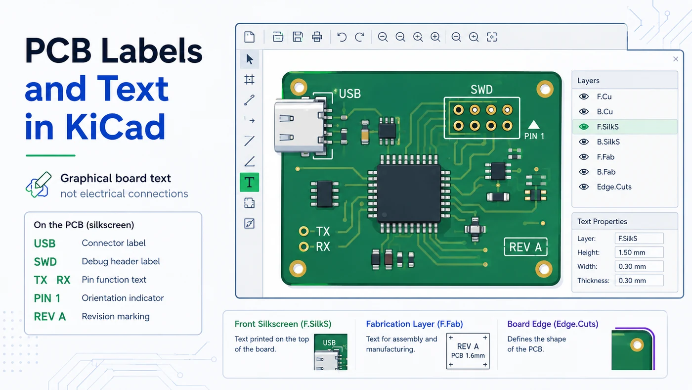
Step-by-Step Instructions
- Open the PCB Editor.
- Select the target layer.
- Press Ctrl + Shift + T or choose the text tool.
- Enter the required text.
- Set the layer, size, stroke thickness, alignment, and rotation.
- Enable mirroring only when appropriate.
- Click OK.
- Place the text on the board.
| PCB layer | Suitable content |
|---|---|
F.Silkscreen |
Connector names, polarity, user instructions |
B.Silkscreen |
Bottom-side assembly markings |
F.Fab |
Fabrication and component information |
B.Fab |
Bottom-side fabrication details |
User.Drawings |
Mechanical or internal notes |
User.Comments |
Review information |
| Copper layer | Copper graphics requiring clearance review |
Common PCB labels include USB, SWD, TX, RX, PIN 1, 12V IN, board name, hardware revision, and serial-number fields.
Text on a copper layer is still a graphic. It is not assigned to a net and does not electrically connect to pads or tracks.
Before manufacturing, check PCB text in the 3D Viewer and Gerber Viewer. Confirm that the text is not hidden under a component, clipped by the board edge, placed over exposed pads, or drawn below the manufacturer’s minimum silkscreen width.
How to Edit, Move, Rotate, or Delete Labels?
KiCad uses consistent shortcuts for most label and text objects.
- E: Edit properties
- M: Move
- G: Drag while maintaining connected geometry where applicable
- R: Rotate
- Delete: Remove the object
You can also double-click a label or right-click it and open Properties.
After moving or rotating an electrical label, verify that its connection point is still attached to the intended wire. KiCad also provides Change To commands for converting some label types without deleting and recreating them.
Label Naming Best Practices
Good names make schematic review and PCB routing faster.
Use Functional Names
Prefer:
MOTOR_ENABLEBATTERY_SENSESPI_MISOFAN_PWMUSB_VBUS
Avoid vague names such as SIGNAL1, WIRE_A, or CONTROL.
Keep One Naming Style
Choose a consistent format, such as uppercase words separated by underscores:
SENSOR_INT_NMOTOR_CURRENTCAN_STANDBY
Consistency improves searchability and reduces spelling errors.
Indicate Active-Low Signals
Use a clear suffix such as:
RESET_NCS_NFAULT_N
Limit Global Scope
Use:
- Local labels for same-sheet connections
- Hierarchical labels for parent-child interfaces
- Global labels for genuine project-wide signals
This prevents invisible connections from spreading farther than intended.
Common KiCad Label Problems and Solutions
Matching Labels Do Not Connect
Check whether:
- The spelling and capitalization match
- One label contains an extra space
- Both labels use compatible scope
- The connection point is attached to the wire
- The labels are on the intended sheets
Local labels on different sheets do not connect.
The Label Looks Connected but Is Not
Zoom in and inspect the small connection square. The text may overlap the wire while the actual attachment point remains beside it.
Two Different Labels Are on One Net
A single electrical net should have one final name. Remove the unnecessary label or rename the conflicting labels consistently.
A Hierarchical Sheet Pin Is Missing
Confirm that the hierarchical label exists inside the child sheet. Then use Place → Sync Sheet Pins on the parent sheet.
Bottom-Side PCB Text Looks Mirrored
Bottom-layer text normally appears mirrored in the editor because it is viewed from the board’s bottom side. Verify the final orientation in the 3D Viewer or Gerber Viewer.
Frequently Asked Questions
1. What is the shortcut for adding a label in KiCad?
Press L to place a local net label. Press Ctrl + L for a global label and H for a hierarchical label. PCB graphical text uses Ctrl + Shift + T by default.
2. Do labels with the same name always connect in KiCad?
Their connection depends on scope. Local labels connect within the same sheet. Global labels connect throughout the schematic. Hierarchical labels connect through matching sheet pins between parent and child sheets.
Labels with the same name and located on the same sheet can connect even when their visual label types differ.
3. Should I use global or hierarchical labels?
Use global labels for signals that genuinely apply across the entire project. Use hierarchical labels when a child sheet should expose a defined set of inputs, outputs, and shared connections to its parent sheet.
Hierarchical labels usually provide clearer signal flow in modular designs.
4. Can PCB text connect to a copper track?
No. A graphical text object on a copper layer is not assigned to a net and does not electrically connect to tracks or pads. It is a copper graphic, not a circuit connection.
5. Can I rename a KiCad label after placing it?
Yes. Place the cursor over the label and press E, or double-click it to open its properties. After renaming a label, verify every related instance so that required connections still use matching names.
How Can EBest Circuit Support Your PCB Project?
Once your KiCad schematic and PCB layout are ready, EBest Circuit can review the manufacturing package for PCB prototyping and production. Send the Gerber files, drill data, stackup requirements, quantity, and assembly files when applicable for a quotation.
You may also like







Tags: how do labels work in kicad, how to add labels in kicad, how to create a net label in kicad, how to make labels in kicad, how to use labels in kicad