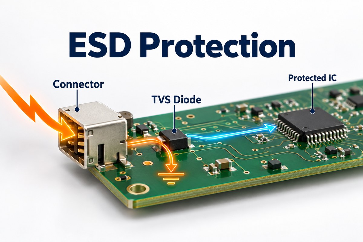
ESD protection limits damage and disruption caused by electrostatic discharge. On a PCB, it typically combines transient voltage suppressor (TVS) diodes at exposed interfaces with short discharge return paths; during assembly, it also requires grounded handling equipment and suitable packaging. A high-kilovolt diode rating alone does not prove that a finished product will pass an ESD test.
For circuit designers, the main decisions are which diode can protect the interface without distorting its signals, where to place it, and how to verify the assembled product.
What Does ESD Protection Protect Against?
ESD protection addresses brief discharges from charged people or objects that can damage semiconductor junctions, reset a controller, or interrupt communication. The discharge may enter through a connector, accessible metalwork, or an exposed board during handling.
| Protection approach | Main purpose | Examples |
| Circuit protection | Limit transient voltage reaching sensitive pins | TVS diodes, diode arrays, coordinated input networks |
| PCB and enclosure design | Control where discharge current flows | Short return paths, connector placement, shielding connections |
| Handling controls | Reduce discharge exposure during production and service | Personnel grounding, dissipative work surfaces, protective packaging |
These approaches address different exposure paths. A wrist strap does not protect a customer’s USB port in use, and a USB protection diode does not protect every exposed component during assembly.
How Does an ESD Protection Circuit Work?
An ESD protection circuit diverts transient current away from the sensitive input, usually through a TVS device connected between the signal and its intended return reference. The TVS is a shunt path, not a series resistor in the signal line.
Toshiba’s TVS operating guidance distinguishes three voltages:
- Working standoff voltage, VRWM: the voltage range in which the device should remain effectively off apart from leakage.
- Breakdown voltage: the point at which significant reverse conduction begins under the specified measurement condition.
- Clamping voltage: the voltage present while the device conducts the specified transient current.
A device marked for a 5.5 V working voltage therefore does not hold every discharge to 5.5 V. The protected pin sees the device’s transient response plus voltage developed across the connection inductance. Protection must be coordinated with the IC’s transient tolerance, using manufacturer guidance and testing rather than the working-voltage number alone.
Which ESD Protection Diodes Fit Your Interface?
High-speed data lines generally need low-capacitance ESD protection diodes, while slower control or audio lines may tolerate more capacitance. Two Texas Instruments parts illustrate the difference without implying that they are interchangeable.
| Parameter | TI TPD4E05U06 | TI TPD1E10B06 |
| Channels | 4 | 1 |
| Working standoff voltage | 5.5 V | ±5.5 V |
| Typical I/O capacitance | 0.5 pF | 12 pF |
| Protection polarity | Unidirectional | Bidirectional |
| Published IEC contact-discharge rating | ±12 kV | ±30 kV |
| Example application category | High-speed interfaces such as USB 3.0 | Audio, buttons, and general-purpose I/O |
Values above are from TI’s product documentation, checked September 15, 2026. Capacitance figures are typical values under datasheet conditions; discharge ratings describe the protection components, not an independently qualified customer PCB.
The 12 pF part has a higher listed contact-discharge rating, but that does not make it the better choice for a high-speed pair. Added loading can degrade signal quality. Check the specific interface’s voltage swing, bandwidth, and channel budget before selecting either device.
Which Ratings Matter Beyond the ESD Voltage?
Working voltage, clamping behavior, capacitance, leakage, and polarity must all match the protected interface; a large ESD withstand number is only one selection input.
- Working voltage: allow for the highest normal line voltage, tolerances, and valid operating modes. A 5.5 V device is not a suitable starting point for a 24 V input.
- Clamping behavior: compare values at the same pulse current and waveform. Do not compare a 1 A clamp specification directly with a much higher-current result.
- Capacitance: review loading on high-speed lines and its variation with bias, not just a headline typical value.
- Leakage: check its effect on high-impedance analog inputs and sensor accuracy, including temperature dependence.
- Polarity and topology: confirm positive and negative signal excursions and whether the device uses a ground clamp or steering paths to a rail.
Toshiba’s selection guidance emphasizes matching device characteristics to the circuit. Package size comes after that electrical fit: a smaller footprint is not useful if its pinout forces a poor discharge path.
When Should You Use an ESD Protection Diode Array?
An ESD protection diode array is useful when several nearby interface lines need protection and the package pinout lets those lines pass through with short, orderly routing. Separate devices can be preferable when the exposed signals are spread across the board or require different voltage ratings.
For an array, verify channel count, pin assignment, shared connections, and the recommended footprint before routing. A four-channel package is not necessarily four identical, independent clamps; its internal schematic determines how it should be connected.
On a differential interface, keep the two signal paths balanced through the protection footprint. Do not protect one line with an extra stub or a substantially different pad arrangement simply because the package is convenient to place.
How Should You Place ESD Protection on a PCB?
Place the protection device close to the exposed connector, bring the signal to its protection connection before continuing toward the IC, and keep the discharge return path short and low-inductance.
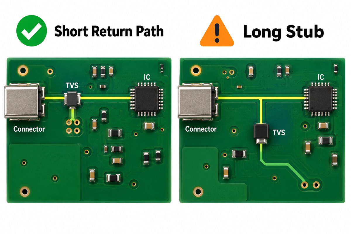
For ESD protection on PCB layouts, Toshiba and TI both emphasize connection inductance. The illustration compares routing concepts; use the selected device’s pinout and reference layout for the actual electrical connections.
- Keep the connector-to-protection segment short and away from sensitive, already-protected traces.
- Avoid a long branch from the signal line to the TVS.
- Place suitable ground vias close to the return pad rather than reaching ground through a long narrow trace.
- Maintain the intended signal reference plane; do not introduce a split under a high-speed pair.
TI’s layout guide shows why fractions of a nanohenry matter: with a current rise of 30 A in 0.8 ns, 0.25 nH contributes approximately 9.4 V through V = L × di/dt. This is an illustrative calculation, not a predicted voltage for every board.
The return must fit the product’s PCB ESD protection strategy. Circuit ground, chassis, and cable shield are not automatically the same node; their connections must respect the interface and any isolation requirements.
How Do HBM, CDM, and System-Level ESD Tests Differ?
HBM and CDM characterize component susceptibility under defined discharge models, while IEC 61000-4-2 evaluates equipment immunity using a different test method. Their kilovolt ratings cannot be substituted for one another.
| Test | Primary subject | Discharge model or purpose |
| HBM: Human Body Model | Electronic component | Charge transferred from a modeled person to a device |
| CDM: Charged Device Model | Electronic component | A charged device discharging through a connection |
| IEC 61000-4-2 | Equipment or system | Immunity to specified direct and indirect ESD exposure |
TI’s system-level design guidance distinguishes component-handling qualification from end-user exposure. Likewise, a TVS tested to an IEC waveform does not certify the enclosure, firmware, cables, and PCB around it.
Choose the applicable product requirements and acceptance criteria before validation. Record contact or air discharge, polarity, test locations, operating modes, and permitted behavior. “No permanent damage” is not the same result as uninterrupted communication.

The laboratory scene is illustrative, not a complete standards-compliant fixture drawing. Equipment placement, insulation, coupling planes, and discharge procedure must follow the applicable test setup.
Why Can a Board Still Fail After Adding a TVS?
A board can still fail when the discharge bypasses the TVS, the clamp voltage exceeds the input’s tolerance, or the return current disturbs another part of the circuit.
- Connector pin damage: inspect the clamp selection and the connector-to-TVS route first.
- Controller reset without visible damage: investigate supply disturbance, reset-line coupling, and ground movement.
- Communication errors: separate transient upset from signal-integrity degradation introduced by the protection footprint.
- Failure only with a particular cable or enclosure: reproduce that configuration and examine its discharge return path.
These are diagnostic starting points, not proof of the root cause. Log the failing location and polarity, change one variable at a time, and retest the relevant operating modes. Increasing the diode’s headline kV rating without checking the current path can leave the fault unchanged.
What ESD Controls Are Needed During PCB Assembly?
Assembly needs personnel grounding, suitable work surfaces, controlled handling materials, and protective packaging because exposed components remain vulnerable before the product enclosure is installed.
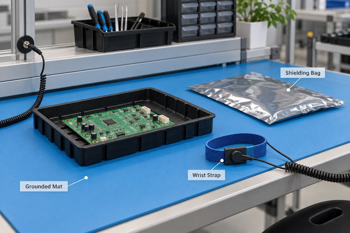
The EOS/ESD Association describes a workstation built around a dissipative surface, personnel grounding, and a common grounding point. Grounding equipment also needs verification; a disconnected or damaged cord cannot be judged by appearance alone.
- Handle exposed assemblies in the designated ESD-protected area.
- Use verified personnel-grounding equipment appropriate to the task.
- Keep unnecessary charge-generating materials away from exposed devices.
- Select packaging for the required low-charging, dissipative, or shielding function.
Our guide to preventing ESD during handling and storage covers those production controls in more detail. Follow the site’s electrical-safety procedures as well; do not improvise a wrist-strap connection to mains wiring.
FAQ About ESD Protection
Does switching off the PCB prevent ESD damage?
No. An unpowered board can still receive a discharge through exposed pins or components. Disconnecting power may be necessary for safe handling, but it does not replace ESD precautions.
Does the highest kV-rated diode provide the best protection?
No. The diode must also limit voltage adequately and preserve normal signal operation. A higher-rated device with excessive capacitance or an inductive connection can be a worse fit for the interface.
Can one diode protect every pin on a connector?
No. Protection follows the connected electrical paths. A device on a supply pin does not automatically clamp the data pins. Map each exposed line to an appropriate channel or protection network.
Do all plastic bags provide ESD protection?
No. Ordinary plastic packaging is not equivalent to qualified ESD packaging, and low-charging material does not automatically provide discharge shielding. Select packaging by its specified function rather than its color.
Should a replacement TVS be approved only by package and voltage?
No. Compare pinout, polarity, clamping data, capacitance, leakage, and the relevant pulse ratings. A replacement can fit the pads yet change signal quality or transient behavior, so assess whether revalidation is needed.
How Can EBest Circuit Support Your PCB Assembly?
At EBest Circuit, we support PCB fabrication, component sourcing, and PCBA assembly, helping you carry the approved protection circuit from the BOM into a buildable board. Share the specified TVS part numbers, placement requirements, and test scope so we can review manufacturing and assembly needs without treating an unapproved substitute as equivalent.
Send your Gerber files, BOM, assembly drawings, quantity, and ESD validation requirements to sales@bestpcbs.com. We can discuss prototyping and production support; any system-level compliance testing must be agreed as a separate, clearly defined project requirement.