To add a new copper layer to KiCad 9, open PCB Editor → File → Board Setup → Board Stackup → Physical Stackup, then increase the copper layer count. For example, changing a two-layer PCB to four layers adds the internal copper layers In1.Cu and In2.Cu.
Adding a copper layer is different from adding a copper zone. A copper layer changes the physical PCB stackup. A copper zone places copper on an existing layer for ground, power, shielding, or current distribution. Knowing which one you need avoids unnecessary setup changes.

How to Add a New Copper Layer to KiCad 9?
To add copper layers in KiCad 9, change the layer count in Physical Stackup.
- Open the PCB layout in PCB Editor.
- Go to File → Board Setup.
- Select Board Stackup → Physical Stackup.
- Find the Copper layers setting.
- Change the board from 2 layers to 4 layers, or select another supported layer count.
- Review the new internal copper layers.
- Click OK.
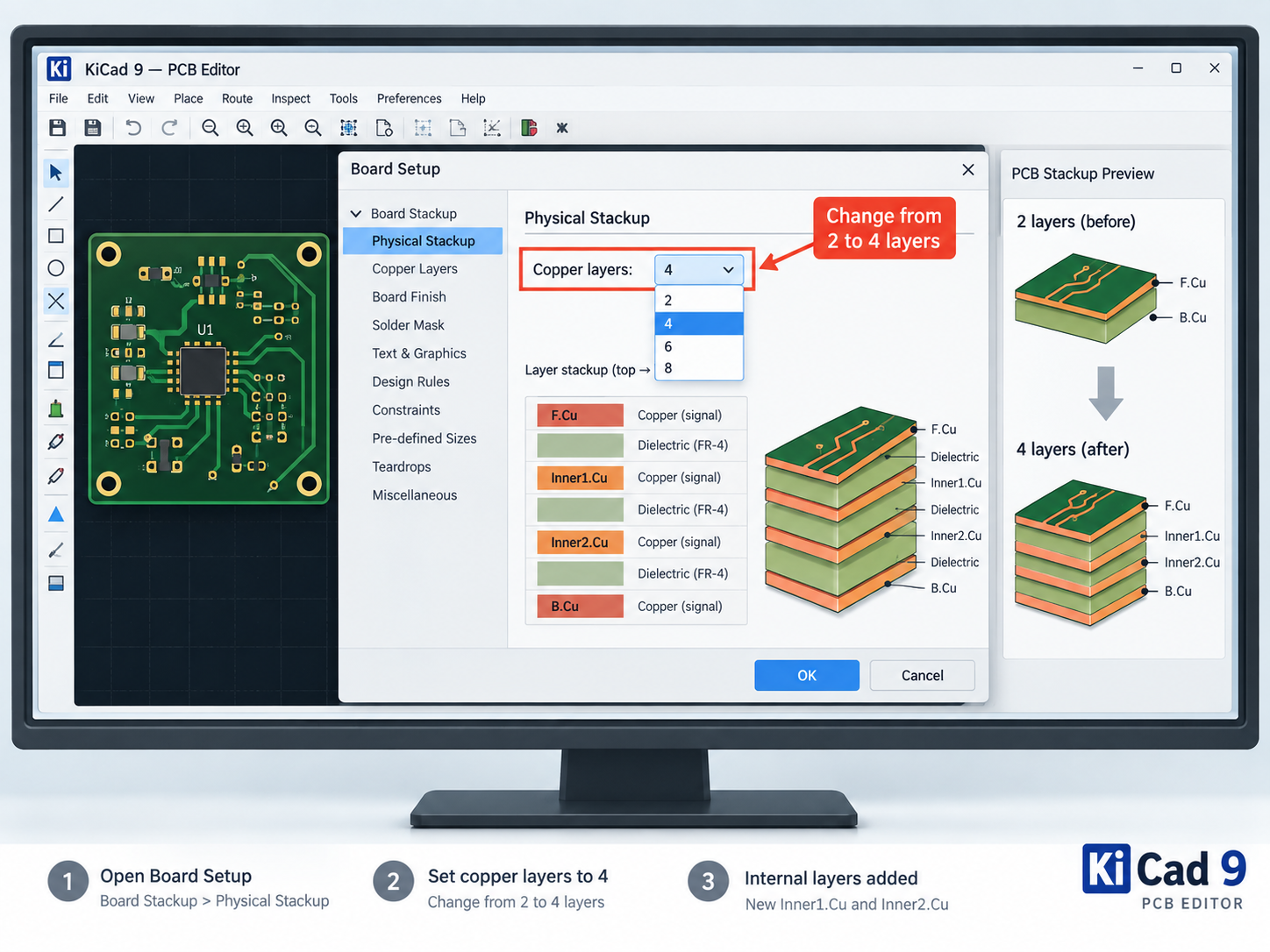
A standard four-layer board will normally include:
F.CuIn1.CuIn2.CuB.Cu
KiCad 9 uses an even number of physical copper layers, so a two-layer design normally moves to four layers rather than three.
After increasing the layer count, check the stackup values instead of treating them as placeholders. Useful items to review include:
- Copper thickness
- Dielectric thickness
- Overall board thickness
- Layer order
- Material type
Do not use Add User Defined Layer to create another electrical copper layer. User-defined layers are intended for drawings, notes, fabrication information, or other non-routing content.
Copper Layer vs Copper Zone in KiCad 9: What Is the Difference?
A copper layer is a physical conductive layer in the PCB, while a copper zone is an area of copper created on an existing layer.
| Item | Copper Layer | Copper Zone |
|---|---|---|
| Main purpose | Adds a physical PCB layer | Adds copper within an existing layer |
| Examples | F.Cu, In1.Cu, In2.Cu, B.Cu | GND pour, power plane |
| Setup location | Physical Stackup | Add Filled Zone |
| Changes PCB layer count | Yes | No |
| Assigned to a net | Not by itself | Usually yes |
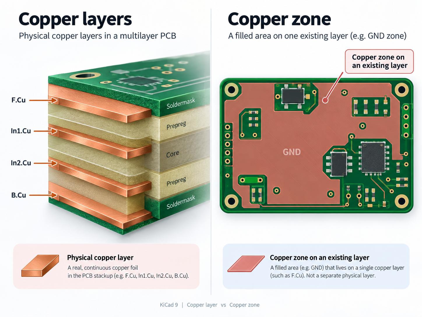
For example, adding In1.Cu gives the PCB another physical copper layer. It does not automatically turn that layer into a ground plane.
If you want In1.Cu to work as ground, create a copper zone on that layer and assign it to the GND net.
This distinction matters because many searches for “how to add copper layer in KiCad” actually come from users who only need a ground or power pour.
How to Add a Ground Plane in KiCad 9?
To add a ground plane in KiCad 9, create a filled copper zone and assign it to the GND net.
- Select the copper layer where the plane should be created.
- Click Add Filled Zone.
- Click inside the PCB outline.
- Select the
GNDnet. - Confirm the target copper layer.
- Draw the zone boundary around the required area.
- Finish the outline.
- Press
Bto refill all zones.
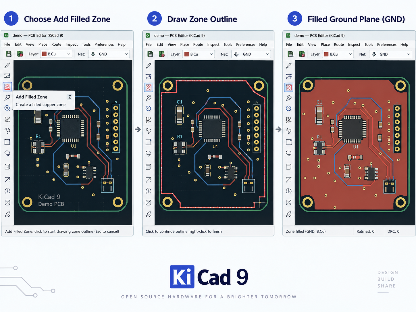
On a two-layer PCB, a GND zone is often placed on B.Cu. On a four-layer board, an internal layer such as In1.Cu may be used as a more continuous ground reference.
The zone boundary only defines where KiCad is allowed to calculate copper. The actual filled shape depends on traces, vias, pads, clearances, cutouts, and design rules. After routing changes, press B again so the copper fill reflects the latest layout.
Which KiCad Copper Zone Properties Should You Set?
The most important KiCad copper zone properties are the net, layer, clearance, minimum width, pad connection, and thermal relief settings.
- Layer: Sets where the zone is placed.
- Net: Connects the zone to GND, power, or another net.
- Clearance: Controls spacing from copper on other nets.
- Minimum width: Removes copper areas that become too narrow.
- Pad connections: Sets solid, thermal relief, or no connection.
- Thermal relief gap: Defines spacing around thermally connected pads.
- Thermal spoke width: Sets the width of each thermal connection.
- Fill style: Selects solid or hatched copper.
- Island removal: Controls how disconnected copper islands are handled.
The values should match both the electrical requirement and the PCB manufacturer’s design rules. Clearance and minimum width deserve particular attention because they can directly change the final filled geometry.
Thermal relief settings also affect assembly. A large solid copper plane can pull heat away from a pad during soldering, while thermal spokes reduce that heat transfer.
How Does KiCad Zone Priority Work?
KiCad zone priority controls which overlapping copper zone is filled first.
A higher-priority zone is calculated before a lower-priority zone. The lower-priority zone then keeps the required clearance from the copper already created.
A common example is:
- A large
GNDzone across most of the layer - A smaller
+5Vzone inside part of the same area
If the +5V area must remain inside the larger ground region, the power zone can be given a higher priority.
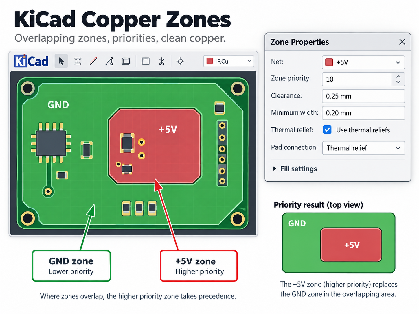
Zone priority is useful when two or more copper zones intentionally overlap. It is not a fix for an incorrect net, poor outline, or unsuitable clearance setting.
If overlapping zones behave unexpectedly, check:
- Net assignment
- Target layer
- Zone outline
- Clearance
- Priority value
For layouts with several zones, the Zone Manager makes it easier to compare their settings in one place.
Why Is the KiCad Ground Plane Not Filling?
If a KiCad ground plane is not filling, press B first to refill all zones.
If the problem remains, check:
- Wrong net: Confirm that the zone is assigned to
GND. - Wrong layer: Make sure the zone is on the copper layer you are viewing.
- Incomplete outline: Check that the zone boundary is closed.
- Large clearance: Too much spacing can remove copper from narrow areas.
- Large minimum width: Narrow copper sections may be discarded.
- Keepout or rule area: These may block copper from filling.
- Board cutout: Copper will not fill through cutouts or outside the board edge.
- Island removal: Small disconnected copper areas may be removed automatically.
- Hidden fill display: The zone may be filled but only its boundary is visible.
If only one section of the plane is missing, inspect that local area closely. Dense vias, BGA fanout, narrow board sections, or nearby keepouts often create the problem. After making changes, refill the zones and run DRC again.
How to Hide Filled Zones in KiCad Without Deleting Them?
To hide filled zones in KiCad, switch the PCB Editor to show only the zone boundaries.
This changes the display only. It does not remove the copper zone from the design.
- Hide zone fill: Keeps the zone but hides the rendered copper.
- Unfill zone: Removes the calculated fill until it is filled again.
- Delete zone: Removes the zone object completely.
Hiding the fill is useful when large power or ground areas make routing difficult to see. If a copper zone suddenly appears to be missing but its outline is still visible, check the display mode before changing the design.
What Should You Check Before Fabricating a Multilayer KiCad PCB?
Before fabricating a multilayer KiCad PCB, confirm that the KiCad stackup matches a stackup your PCB manufacturer can actually build.

Check these items before releasing fabrication data:
- Copper layer count: Make sure all intended layers are included.
- Layer order: Confirm the correct position of signal, ground, and power layers.
- Board thickness: Verify the finished PCB thickness.
- Copper thickness: Confirm outer- and inner-layer copper requirements.
- Dielectric structure: Review core and prepreg thicknesses.
- Controlled impedance: Confirm material, dielectric thickness, copper thickness, and target impedance.
- Via structure: Check through holes, blind vias, buried vias, or microvias.
- Plane continuity: Look for fragmented ground or power planes.
- Zone fill: Press
Bbefore final output. - DRC: Resolve relevant clearance and connectivity errors.
- Gerber and drill data: Confirm that every copper and drill layer is exported correctly.
A four-layer board created in KiCad is not automatically a production-ready four-layer stackup. The PCB factory may use different prepreg thicknesses, core materials, or copper weights from the default CAD values.
For controlled-impedance boards, confirm the production stackup before finalizing critical trace widths. A dielectric change can alter the impedance even when the routing geometry stays the same.
If your KiCad design is ready for fabrication, EBest Circuit can review the Gerber files, stackup, material selection, copper weight, via structure, and impedance requirements before production.
For schematic net naming, see our guide to how to make labels in KiCad.
FAQ About Adding Copper Layers in KiCad 9
1. Can I add only one new copper layer in KiCad 9?
No. KiCad 9 uses an even number of physical copper layers, so a two-layer PCB normally changes to four layers rather than three.
2. How do I change a KiCad PCB from 2 layers to 4 layers?
Open PCB Editor → File → Board Setup → Board Stackup → Physical Stackup, then change the copper layer count from 2 to 4.
3. Is In1.Cu automatically a ground plane in KiCad?
No. In1.Cu is only an internal copper layer. Create a copper zone on it and assign that zone to GND if you want to use it as a ground plane.
4. What is the shortcut to refill copper zones in KiCad?
Press B to refill all copper zones.
5. Why did my copper fill disappear in KiCad?
The fill may be hidden, unfilled, blocked by clearance rules, or removed by zone settings. Check the display mode first, then refill the zone with B.
6. Can one copper zone be used on multiple layers in KiCad 9?
Yes. A zone can be assigned to multiple copper layers while using the same net, with the copper fill calculated separately on each selected layer.
Adding a new copper layer in KiCad 9 is simple once you use the correct stackup settings. The more important step is making sure the final layer structure, zones, vias, and fabrication data match the PCB you actually want to manufacture.