An H bridge circuit is a four-switch circuit that reverses the voltage across a load, allowing a DC motor to run forward or backward. It can also support PWM speed control, braking, and bidirectional current control. A typical full H bridge uses four MOSFETs or transistors arranged around the motor.
The basic circuit is simple, but a reliable H bridge design depends on correct MOSFET selection, gate timing, stall current, inductive protection, PCB current paths, and heat dissipation. These details become especially important when a schematic moves into an actual H bridge circuit board.
What Is an H Bridge Circuit and What Is It Used For?
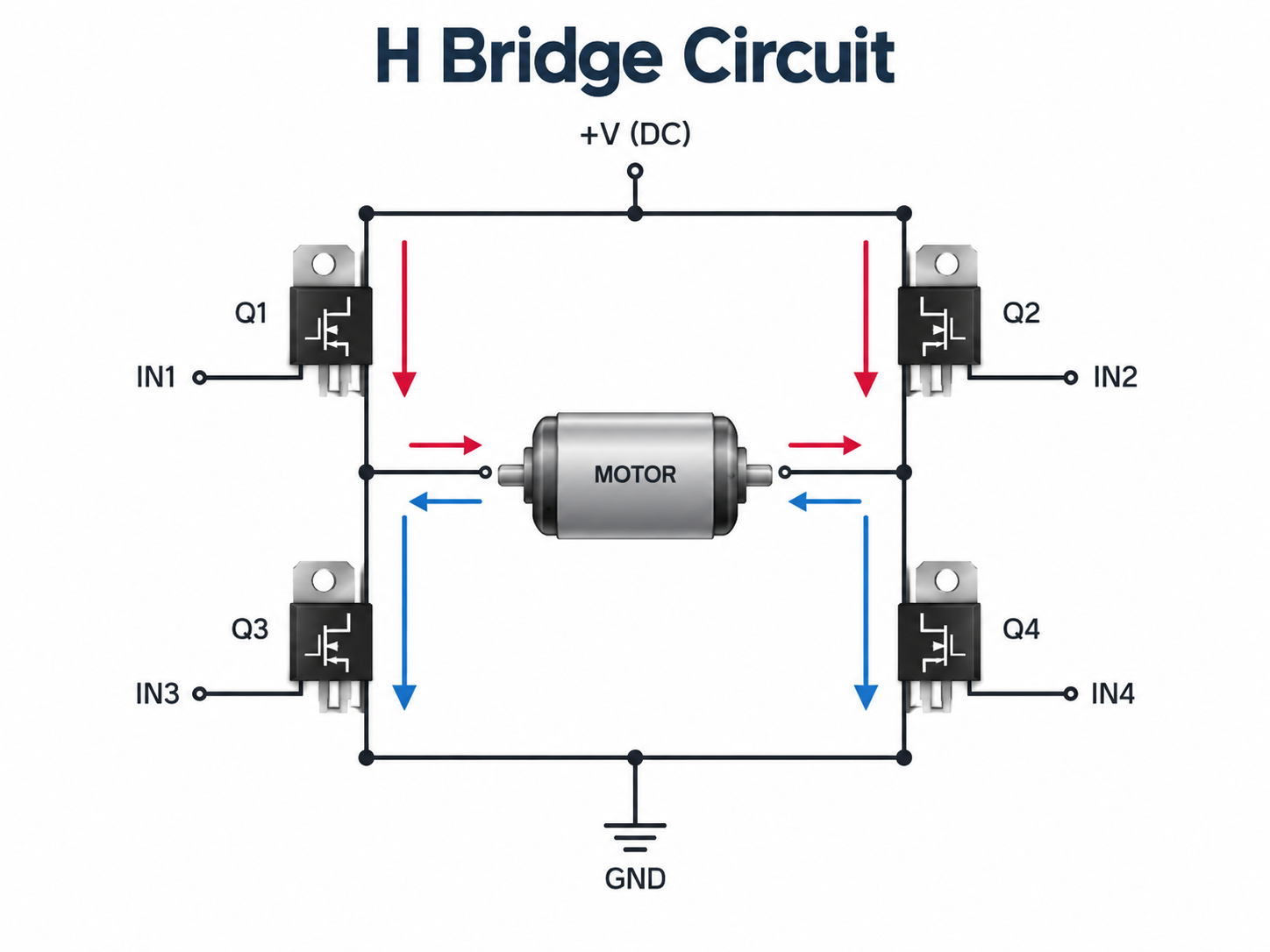
An H bridge circuit controls the direction of current through a load by switching its two terminals between the power supply and ground.
The circuit normally contains:
- Two high-side switches
- Two low-side switches
- A DC supply
- A load connected between the two switching legs
- Control signals for the four switches
Its name comes from the traditional circuit diagram. The four switching devices form the sides of an imaginary “H,” while the motor or load sits across the center.
The main purpose of an H bridge is polarity reversal. Instead of physically swapping the wires connected to a DC motor, the switches reverse the voltage across the motor electronically.
Common applications include:
- DC motor forward and reverse control
- PWM motor speed control
- Motor braking
- Solenoids and actuators
- Robotics and motion systems
- Bidirectional current control
- Class-D output stages
- DC-to-AC inverter stages
For a brushed DC motor, reversing armature current reverses motor rotation. That is why the H bridge has become a standard circuit in motor-control electronics.
What Does an H Bridge Circuit Diagram Show?
An H bridge circuit diagram shows four switches arranged in two legs, with the motor connected between the two switching nodes.
A typical MOSFET H bridge includes:
- Q1: left high-side MOSFET
- Q2: left low-side MOSFET
- Q3: right high-side MOSFET
- Q4: right low-side MOSFET
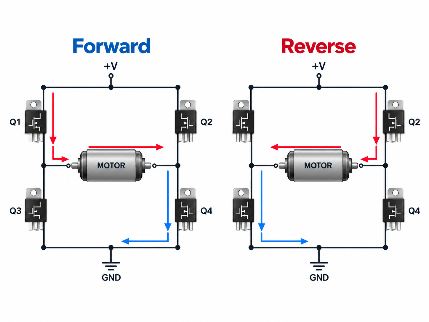
The circuit changes motor polarity by turning on opposite diagonal MOSFETs.
| Active MOSFETs | Left Motor Terminal | Right Motor Terminal | Result |
|---|---|---|---|
| Q1 + Q4 | High | Low | Current in one direction |
| Q2 + Q3 | Low | High | Current in the opposite direction |
| All OFF | Floating | Floating | Coast |
| Both motor terminals at the same potential | Same | Same | Brake |
Switch labels differ between schematics, so it is more useful to follow the current path than memorize Q1, Q2, Q3, and Q4 positions.
One switching rule is critical: the high-side and low-side MOSFET in the same leg must not conduct at the same time. Otherwise, they can create a direct path from the supply rail to ground. This condition is called shoot-through.
How Does an H Bridge Circuit Work for a DC Motor?
An H bridge controls a DC motor by reversing the voltage polarity across its two terminals.
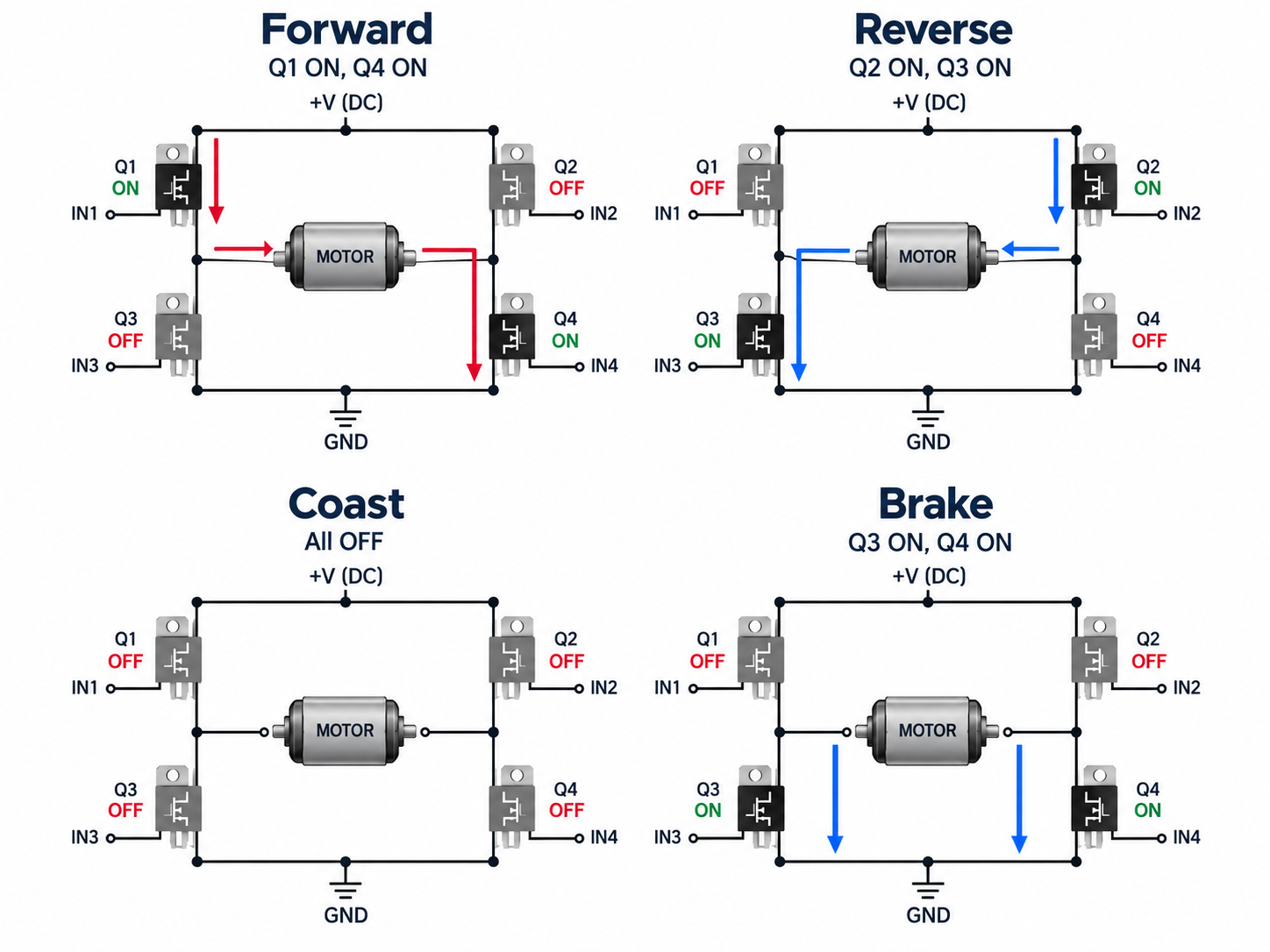
For forward rotation, one high-side MOSFET and the diagonally opposite low-side MOSFET conduct. Current flows through the motor in one direction.
For reverse rotation, the opposite diagonal pair turns on. The motor current reverses, so the motor rotates the other way.
| H Bridge State | Switching Condition | Motor Response |
|---|---|---|
| Forward | First diagonal pair ON | Forward rotation |
| Reverse | Opposite diagonal pair ON | Reverse rotation |
| Coast | All switches OFF | Motor slows freely |
| Brake | Motor terminals held at similar potential | Faster deceleration |
PWM is normally used when speed control is also required. The controller rapidly switches the bridge and changes the duty cycle to adjust the average voltage applied to the motor.
Motor current should be checked carefully before selecting the power stage. Important values include:
- Normal running current
- Startup current
- Stall current
- Current during rapid direction reversal
- Expected PWM duty cycle
Stall current is particularly important because it can be several times higher than normal operating current. MOSFETs, PCB copper, connectors, and the power supply must all tolerate this condition.
Half H Bridge vs Full H Bridge Circuit: What Is the Difference?
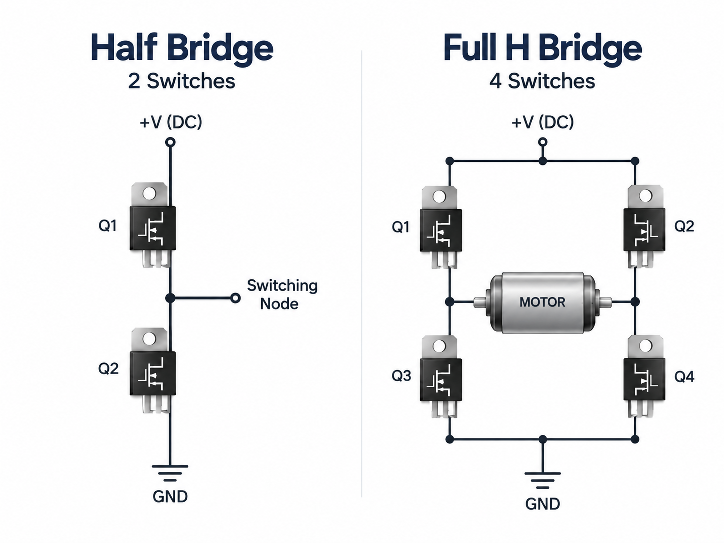
A half bridge uses one pair of switches, while a full H bridge uses two half-bridge legs and normally contains four switches.
| Feature | Half Bridge | Full H Bridge |
|---|---|---|
| Main switches | 2 | 4 |
| Switching legs | 1 | 2 |
| Output | One switched midpoint | Two switched midpoints |
| Load polarity reversal | Not by itself | Yes |
| DC motor reversing | Requires additional circuitry | Directly supported |
| Typical applications | Power conversion, inverter legs | Motors, actuators, full-bridge inverters |
In a half bridge, the output switches between the upper and lower supply rails.
A full H bridge places the load between two half-bridge switching nodes. Because either side of the load can be driven high or low, the voltage across it can be reversed.
For this reason, a full H bridge is normally used when a DC motor needs both forward and reverse operation.
How Do You Design an H Bridge Circuit Using MOSFETs?
A MOSFET H bridge should be designed from the actual supply voltage, motor current, switching frequency, and thermal conditions.
The most important MOSFET parameters are below.
Drain-source voltage
The MOSFET VDS rating must exceed the highest voltage it may see in operation, including supply tolerance and switching overshoot.
Motor windings are inductive, so the peak drain voltage can be higher than the nominal DC bus voltage.
Current rating
Do not size the MOSFET from running current alone. Check:
- Continuous motor current
- Startup current
- Stall current
- Short-duration peak current
- Expected board and ambient temperature
Datasheet current ratings are strongly affected by package temperature and PCB thermal conditions.
RDS(on)
MOSFET conduction loss can be estimated with:
Low RDS(on) becomes increasingly important as motor current rises. Use the resistance expected at the real junction temperature rather than relying only on the 25°C typical value.
Gate charge
Gate charge affects how quickly the MOSFET can switch. A device with very low RDS(on) may have a larger gate charge, which requires more current from the gate driver. Slow transitions increase switching loss.
High-side drive
A high-side N-channel MOSFET usually needs a gate voltage above its source voltage.
Common drive methods include:
- Bootstrap gate drivers
- Charge-pump drivers
- Isolated gate-driver supplies
Low-voltage circuits sometimes use P-channel MOSFETs on the high side because they are easier to drive, although their RDS(on) is often higher.
PWM frequency
PWM frequency affects both control behavior and switching loss. A higher frequency may move switching noise above the audible range, but it also increases switching events per second.
The final choice should suit the motor, MOSFET, driver, and thermal budget rather than being selected in isolation.
How Do You Prevent Shoot-Through and Inductive Voltage Spikes?
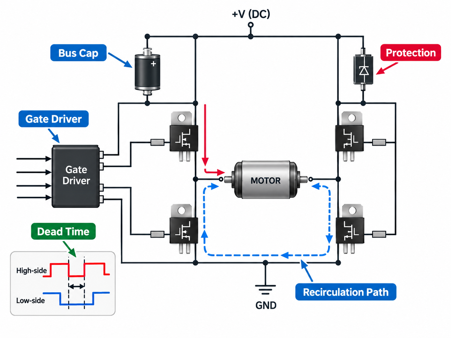
Shoot-through is controlled with correct gate timing, while inductive voltage spikes are controlled by giving motor current a safe path when the MOSFETs switch.
Shoot-through prevention
Shoot-through happens when both MOSFETs in the same bridge leg conduct simultaneously.
Possible results include:
- Very high supply current
- MOSFET overheating
- Gate-driver damage
- Supply voltage collapse
- PCB or connector damage
The usual solution is dead time. One MOSFET is allowed to turn fully off before the complementary MOSFET turns on.
Required dead time depends on:
- MOSFET switching characteristics
- Gate charge
- Gate resistance
- Driver source and sink current
- Propagation delay
Too little dead time risks cross-conduction. Too much increases body-diode conduction and power loss.
Inductive voltage control
Motor current cannot stop instantly when a MOSFET turns off. The stored magnetic energy must continue flowing through another path.
Depending on the design, this path may use:
- MOSFET body diodes
- External diodes
- Synchronous MOSFET conduction
- TVS devices
- Snubber circuits
- Local bus capacitors
The protection components should be selected from the actual motor current and measured switching waveform, not only from the nominal supply voltage.
H Bridge IC vs Discrete MOSFETs: Which Should You Use?
An H bridge IC is usually easier for compact low- or medium-power designs, while external MOSFETs provide more flexibility for higher-current applications.
| Design | Best Fit |
|---|---|
| Integrated H bridge IC | Compact, lower-power designs |
| Driver IC + external MOSFETs | Medium- to high-power motor control |
| Discrete bridge | Highly customized power stages |
An integrated H bridge IC may include:
- Power switches
- Gate drivers
- Overcurrent protection
- Thermal shutdown
- Undervoltage lockout
- Current sensing
- Fault reporting
This reduces component count and simplifies the PCB.
External MOSFETs are useful when the design requires:
- Higher motor current
- Higher bus voltage
- Lower conduction loss
- Better heat spreading
- Specific MOSFET packages
- Custom switching behavior
Many practical motor controllers use a gate-driver IC with four external N-channel MOSFETs. This keeps the control function integrated while allowing the power devices to be selected separately.
What PCB Layout Rules Matter for an H Bridge Circuit Board?
An H bridge circuit board should keep high-current and high-speed switching paths short while separating noisy switching nodes from sensitive control signals.
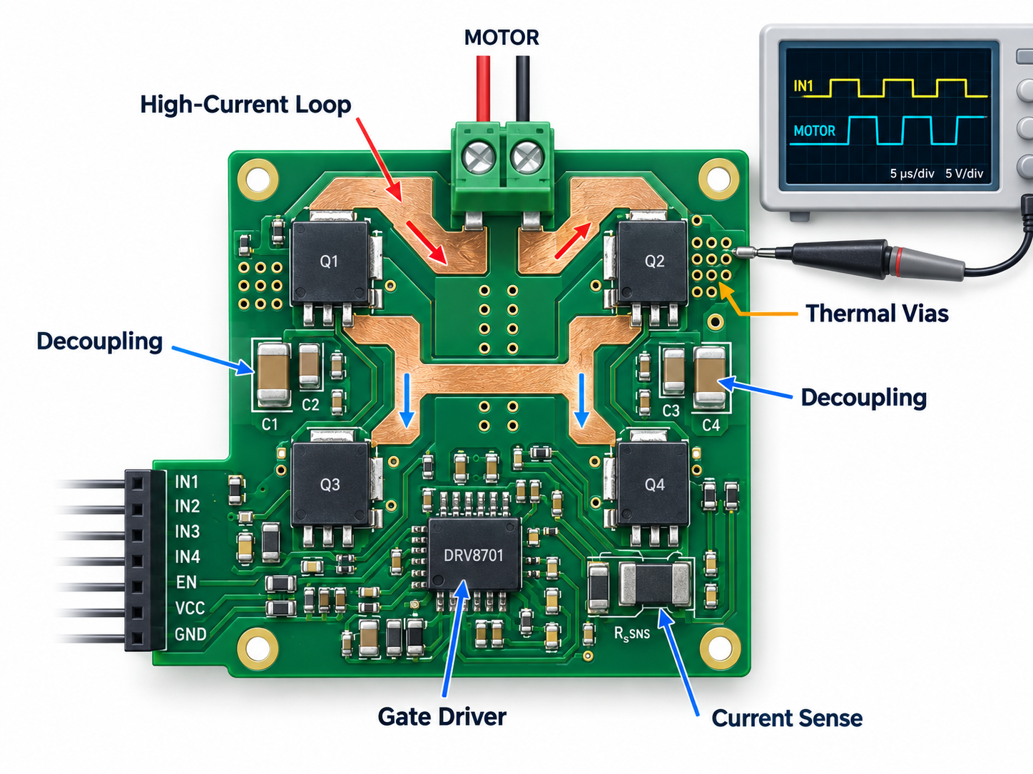
The most important PCB layout rules are:
- Keep the DC bus switching loop compact.
- Place local ceramic decoupling close to the MOSFET bridge.
- Keep gate-driver traces short.
- Provide a direct gate-return path.
- Keep switching-node copper away from analog and control signals.
- Size power copper for peak motor current, not only running current.
- Provide adequate thermal copper under power MOSFETs.
- Use thermal or current-sharing vias where required.
- Route current-sense connections separately from motor current paths.
The bus capacitor is especially important. If it is too far from the MOSFET bridge, the extra trace inductance can increase drain-voltage ringing.
High-current H bridge boards may require more than ordinary trace widening. Depending on current and thermal limits, the PCB can use:
- Large copper pours
- Heavier copper
- Parallel copper layers
- Dense via arrays
- Copper inlays or busbars
Switching-node copper should be large enough for electrical and thermal needs but not unnecessarily oversized. Large high-dV/dt areas increase capacitive coupling and EMI.
Current-sense circuits also deserve careful routing. Kelvin connections should be used where a low-value shunt resistor is measured, and its sense traces should be kept away from fast switching nodes.
How Do You Simulate and Test an H Bridge Circuit?
H bridge simulation should verify switching timing and device stress, while prototype testing should confirm the actual waveforms, current, and temperature on the assembled PCB.
Useful simulation results include:
- High-side and low-side gate waveforms
- Dead time
- Motor current
- Current reversal
- PWM behavior
- Switching-node voltage
- Drain-source voltage
- Voltage overshoot
- MOSFET power loss
- DC bus ripple
Ideal switch models are useful for learning the basic H bridge operation, but realistic MOSFET and diode models are more useful when checking switching loss or transient behavior.
After assembly, test the board under realistic operating conditions.
Typical measurements include:
- MOSFET gate-source voltage
- Bridge switching-node waveform
- Motor startup current
- Stall or near-stall current
- Direction-reversal behavior
- DC bus overshoot
- MOSFET temperature
- Connector and copper temperature
Testing should cover the expected supply voltage, motor load, PWM duty cycle, ambient temperature, and operating time.
A motor that runs correctly at no load does not prove that the H bridge can handle startup, stall, braking, or repeated direction changes.
Use appropriate measurement equipment when probing high-side or floating switching nodes. A differential probe or isolated measurement method may be required to avoid creating an accidental short through the oscilloscope ground.
FAQ
1. Why is it called an H bridge circuit?
Because the traditional circuit diagram resembles the letter H. Four switches form the sides, and the motor or load connects across the middle.
2. Can an H bridge control motor speed and direction?
Yes. The H bridge reverses motor direction by changing polarity, while PWM controls the average voltage used for speed control.
3. What is the difference between a half bridge and a full H bridge?
A half bridge has one switching leg with two switches. A full H bridge has two switching legs and normally four switches, allowing the load voltage to reverse.
4. What causes shoot-through in an H bridge circuit?
Shoot-through occurs when the high-side and low-side MOSFET in the same leg conduct at the same time. Proper dead time prevents this condition.
5. Can an H bridge circuit be used as an inverter?
Yes. A full H bridge can alternate the polarity across a load and is commonly used in inverter power stages.
6. What is a dual H bridge circuit?
A dual H bridge contains two independent H bridge channels. It can drive two bidirectional DC motors or other loads from one circuit or IC.
Need Support With an H Bridge PCB or PCBA Project?
An H bridge PCB has to carry motor current while controlling fast switching edges, heat, gate timing, and inductive transients within the same board.
EBest Circuit supports PCB fabrication and PCBA for motor-control and power-electronics projects. If you are preparing an H bridge circuit board, send your Gerber files, BOM, schematic or fabrication drawing, operating voltage, motor current, and quantity to sales@bestpcbs.com for engineering review and quotation.