





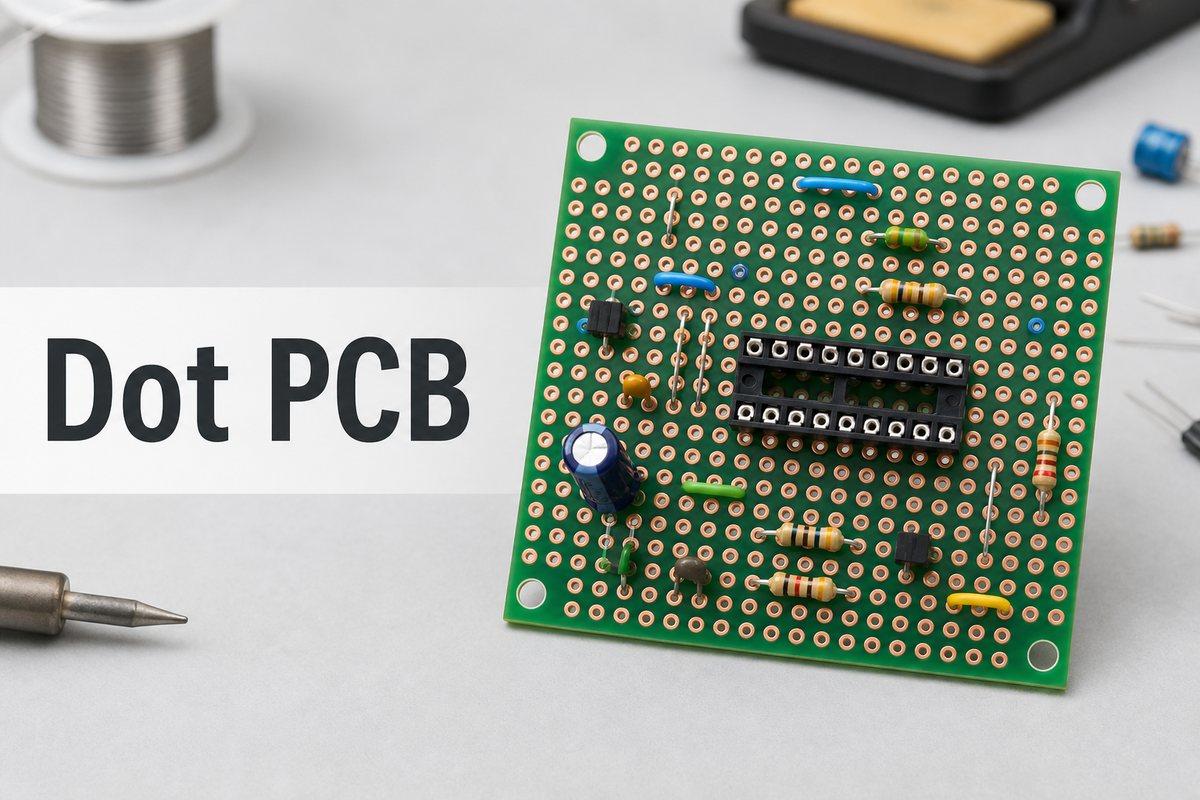
A Dot PCB is a solderable prototyping board with a regular hole grid and an individual copper pad around each hole. Unlike stripboard, neighboring holes are normally not connected, so the builder creates every electrical node with component leads, jumper wire or carefully controlled solder links. It is useful for simple through-hole prototypes, but it does not provide the repeatability, routing control or production readiness of a custom PCB.
This guide focuses on the details that determine whether a dot board works reliably: pad pattern, component-side versus copper-side orientation, node planning, soldering, inspection and the point at which manual wiring should become a manufactured circuit board.
What Is a Dot PCB?
A Dot PCB is a general-purpose perfboard used to build soldered electronic prototypes without designing a custom copper pattern first. Each hole acts as a mechanical mounting point, while its surrounding copper pad provides a solderable land for a component lead or wire.
The board is most suitable for small, low-speed, through-hole circuits such as LED indicators, sensor interfaces, simple timers, relay drivers and microcontroller support circuits. It is less suitable when current, noise, frequency, geometry or repeatability must be tightly controlled.
Dot PCB Full Form and Common Names
The search phrase dot pcb full form does not expand into a separate formal engineering term. The word Dot describes the visible grid of isolated copper dots, while PCB means printed circuit board. Depending on the market, the same or a closely related product may be sold as:
- Dot board or dotted PCB
- Pad-per-hole perfboard
- Zero PCB
- Universal prototyping board
- Solderable protoboard
These names are not always interchangeable. A stripboard has continuous copper tracks, while a breadboard-pattern solder board copies the hidden connection groups of a solderless breadboard. Check the copper side instead of relying only on the product name.
How Does a Dot PCB Board Connect Components?
A dot pcb board does not create a circuit merely by holding parts. Every electrical connection must be deliberately formed between isolated pads. Common methods include insulated jumper wire, tinned solid wire, bent component leads and short solder bridges used only where spacing and inspection remain manageable.
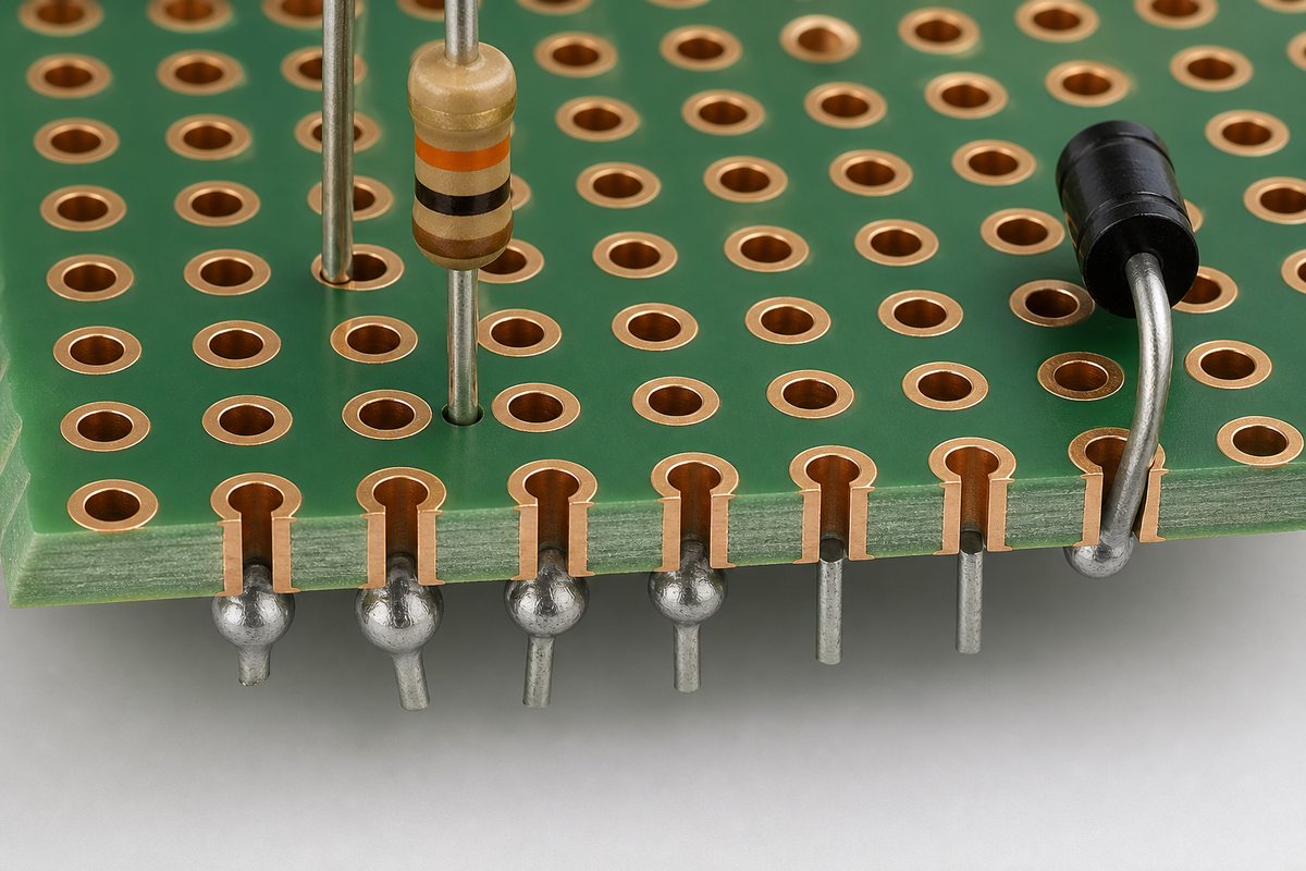
Plan each net as a group of points that must be electrically common. Power and ground paths deserve special attention because a long chain of small solder links can be difficult to inspect and may not suit the required current. Use wire of an appropriate gauge, provide mechanical support at connectors and keep sensitive signal paths away from switching or high-current wiring.
Which Materials and Pad Patterns Are Common?
Dot boards are commonly sold in paper-phenolic and fiberglass-reinforced laminate versions, with copper pads on one side or both sides. Product listings often use a 2.54 mm grid because it matches many through-hole IC sockets, headers and discrete components, but the actual pitch, hole diameter and pad size must be checked before purchase.
| Board feature | What to verify | Why it matters |
| Base material | Phenolic or fiberglass laminate | Changes stiffness, heat tolerance and durability during rework |
| Copper pattern | Isolated pads, strips or breadboard-style groups | Determines which holes are already connected |
| Copper sides | Single-sided or double-sided | Affects access, anchoring and routing options |
| Pitch and hole size | Match component leads and headers | Prevents forced insertion and poor mechanical support |
| Board dimensions | Usable grid area and mounting holes | Controls component spacing and enclosure fit |
Dot PCB vs Stripboard vs Breadboard: What Changes?
The main difference is how the holes are electrically connected. A Dot PCB normally leaves every pad isolated, stripboard connects holes along copper strips, and a solderless breadboard uses reusable spring contacts arranged in hidden groups.
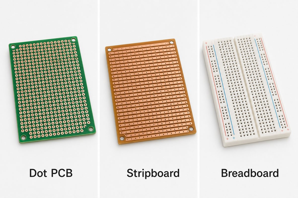
| Board type | Connection pattern | Best use | Main limitation |
| Dot PCB | Individual copper pads | Flexible soldered through-hole prototypes | Every net must be wired manually |
| Stripboard | Continuous copper strips | Ordered layouts that follow row-based routing | Tracks must be cut where isolation is required |
| Breadboard | Reusable internal spring contacts | Fast experiments and component-value changes | Loose wiring and limited mechanical stability |
| Custom PCB | Designed copper traces and planes | Validation, repeatability and production | Requires design files and fabrication |
For a broader development-stage comparison, see our proto board guide. The important purchasing check is the underside pattern: product photos of the component side alone may not reveal whether pads are isolated or connected.
How Should You Plan a Dot PCB Layout Before Soldering?
Plan the layout from the schematic before installing parts. A hand-wired prototype becomes difficult to debug when component placement is improvised while soldering.
- Mark the board orientation. The copper-side view is mirrored relative to the component side. Choose one reference corner and keep it consistent.
- Place fixed mechanical items first. Position connectors, switches, displays, sockets and mounting holes before small passives.
- Group components by circuit block. Keep the input, power regulation, controller and output sections visually distinct.
- Map power and ground nodes. Decide wire gauge, return paths and connection points before adding signals.
- Keep decoupling components close. Place each required bypass capacitor near the device pins it supports.
- Reserve test access. Leave points for ground, supply rails and important signals.
- Check the mirrored plan. Compare the component-side sketch with the copper-side connections before soldering.
A photo or marked drawing of both sides becomes useful design evidence later. It helps convert the prototype into a schematic and then into a controlled PCB layout.
How Do You Perform Dotted PCB Soldering?
Dotted pcb soldering works best when each joint is completed as a controlled pad-and-lead connection, followed by a separate wiring step. Do not attempt to draw long tracks with oversized solder blobs.
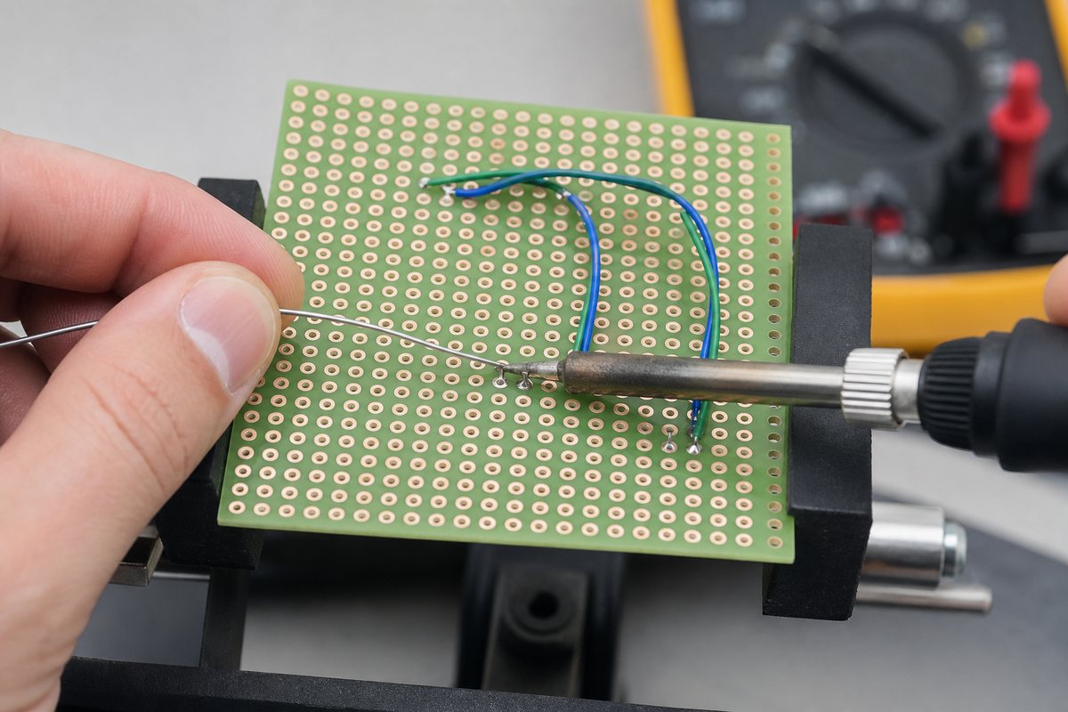
- Work on an unpowered board and secure it in a holder.
- Confirm component value, pinout and polarity before insertion.
- Touch the clean, tinned iron tip to the pad and lead together.
- Feed electronics solder into the heated joint, not directly onto the iron.
- Stop once solder has wetted both surfaces and formed a controlled fillet.
- Remove the solder, then the iron, and keep the joint still while it cools.
- Trim the lead only after inspection, without pulling against the pad.
- Add jumper wires one net at a time and check continuity as the build progresses.
Our detailed guide on how to solder a PCB circuit board covers tool selection, joint inspection, rework limits and electrical safety in more depth.
Which Tools and Materials Are Needed?
A small, controlled tool set is safer than improvising with an oversized iron and plumbing materials. Prepare:
- A temperature-controlled soldering iron with a tip suited to the pad size
- Electronics solder and compatible electronics flux
- A stable PCB holder, safety glasses and fume extraction
- Flush cutters, wire strippers and ESD-safe tweezers
- Insulated solid-core wire and appropriately sized power wire
- Magnification, a multimeter and a current-limited bench supply
- Solder wick or a suitable desoldering tool for corrections
The correct iron setting depends on alloy, tip geometry, pad size, wire mass and board material. Follow the solder and component guidance, then use the lowest practical setting that produces prompt wetting without prolonged contact.
What Common Dot PCB Faults Should You Check?
The most common failures are unintended shorts, open connections, mirrored-layout mistakes and mechanically weak wiring. Inspect the board before power-up and again after every repair.
- Solder bridge: adjacent isolated pads are connected unintentionally.
- Cold or poorly wetted joint: solder sits on the surface without bonding to both pad and lead.
- Wrong-side routing: a copper-side connection was placed incorrectly because the mirrored view was not considered.
- Lifted pad: excessive heat or mechanical force separates copper from the laminate.
- Unsupported wire: movement transfers stress directly to a small solder joint.
- Polarity or pinout error: a diode, capacitor, transistor or IC was installed in the wrong orientation.
- Hidden short under a component: clipped leads or bare wire touch where visual access is poor.
Check power-to-ground resistance, required continuity and unintended connections while the board is unpowered. Initial power-up should use an appropriate current limit when the circuit permits it.
When Is a Dot PCB Perfboard the Right Choice?
A dot pcb perfboard is the right choice when the circuit is small, uses accessible through-hole parts, operates at modest speed and power, and only one or a few hand-built units are needed.
It is particularly useful for educational builds, simple interface circuits, quick fixtures, one-off adapters and proof-of-concept hardware that needs stronger connections than a solderless breadboard. It also gives the designer freedom to arrange irregular through-hole parts without cutting stripboard tracks.
The choice becomes less attractive as wire count, assembly time, test requirements or unit quantity increase. A low board price does not compensate for hours of manual wiring and troubleshooting.
Which Circuits Should Not Stay on a Dot PCB?
A Dot PCB should not be treated as a production substitute when electrical or mechanical behavior depends on controlled geometry. Move to a custom PCB when the design involves:
- High-speed digital interfaces or controlled-impedance signals
- RF circuits, antennas or tightly controlled return paths
- Precision analog signals vulnerable to leakage, coupling or ground error
- High current, high voltage or significant thermal dissipation
- Fine-pitch SMD, QFN, BGA or dense mixed-technology assembly
- Defined creepage, clearance, enclosure or connector geometry
- Repeated builds that must behave consistently
- Formal inspection, traceability or product qualification
A manufactured blank circuit board provides designed copper features, solder mask, silkscreen, drill control and a specified surface finish. Those controls matter once the prototype becomes engineering validation hardware.
What Affects Dot PCB Board Price?
Dot pcb board price is usually influenced by laminate material, dimensions, copper on one or two sides, plating quality, hole count, mounting features, pad finish, supplied accessories, order quantity and local distribution costs.
Compare usable area and construction rather than the lowest listed price alone. A board that sheds pads during rework or does not fit the component pitch can cost more in lost time than the purchase-price difference. For a one-off learning circuit, a basic board may be enough. For a prototype that will be handled or tested repeatedly, fiberglass construction and better-supported holes may be worth considering.
FAQ About Dot PCB
Is every hole on a Dot PCB connected? No. On a typical pad-per-hole board, each copper pad is isolated. Always inspect the copper side or check continuity because some products use strips or breadboard-style groups.
Can a Dot PCB be reused? Components can sometimes be removed and pads reused, but repeated heating can damage the copper and laminate. It is not reusable in the same convenient sense as a solderless breadboard.
Can SMD components be mounted on a dot board? Standard 2.54 mm boards favor through-hole parts. Some larger SMD parts can use adapter boards, but fine-pitch packages need matching pads and better process control.
Are the component side and copper side oriented the same way? No. When the board is flipped, the copper-side view is mirrored. Mark a reference corner and verify pin numbering before making connections.
Should adjacent pads be joined with solder? A very short, intentional bridge may be practical, but long solder tracks are hard to control and inspect. Jumper wire is usually clearer for longer connections.
What files are needed to convert the prototype into a custom PCB? Start with a confirmed schematic, BOM, connector and mechanical requirements, photos or wiring records, and test expectations. Gerber and drill files are then produced from the completed PCB layout.
How Can We Move a Dot PCB Prototype into Production?
At EBest Circuit, we support the step from a working hand-wired prototype to a controlled PCB and PCBA build. Our team can review the schematic, board outline, component footprints, BOM, connector locations, test needs and manufacturing risks before fabrication.
Before requesting a PCB prototype, capture every verified connection on the Dot PCB; do not rely on photos alone when wires overlap or disappear beneath components. Send your schematic, BOM, dimensions, quantity and available prototype records to sales@bestpcbs.com. We can help turn the verified circuit into fabrication files, assembled samples and a repeatable production path.
You may also like







Tags: Dot PCB, dot pcb board, dot pcb board price, dot pcb full form, dot pcb perfboard