PCB manufacturing PCB manufacturing
Home > Blog

PCB feed-through card: Vias, Connectors and Filters

September 11th, 2026

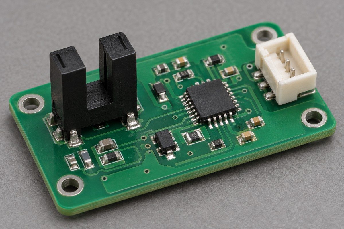
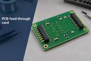
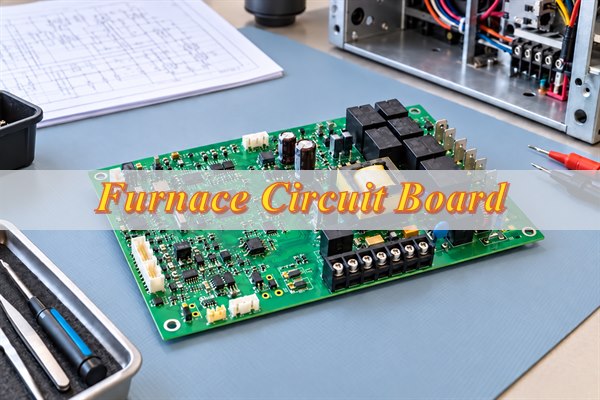
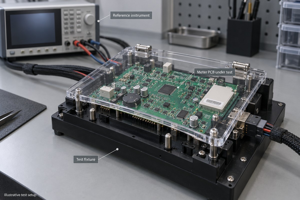
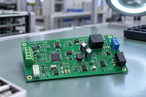
A PCB feed-through card can carry power or signals between connections in an equipment assembly, with filtering added where the circuit needs noise suppression. Understanding that electrical path makes it easier to distinguish the board itself from its connectors, plated holes and filter components—and to choose a replacement that preserves the original function.

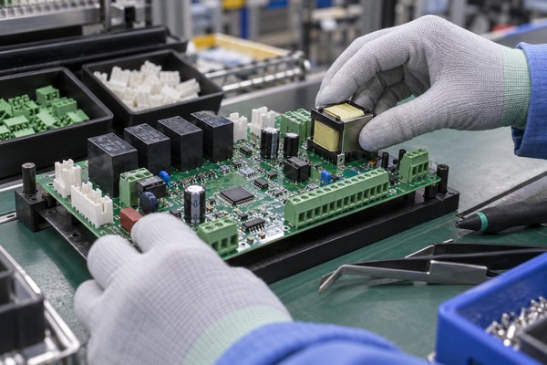
EBest Circuit (Best Technology) combines PCB fabrication and component sourcing with SMT, through-hole and mixed PCB assembly. For a board combining connector pins and small filter components, this means both assembly methods can be handled within the same project. We also support customer-supplied components, giving you the option to retain specified connectors while arranging the remaining procurement and assembly with us. Contact sales@bestpcbs.com to discuss a suitable build option.

PCB feed-through card

What does PCB feed-through card mean?

The phrase is an equipment-specific description: it identifies a board or assembly by its connection function. It does not specify one universal circuit, connector arrangement or pinout. To understand a particular card, distinguish the complete assembly from the features that form its electrical paths.

The board, connection and filter perform different jobs:

  • The card carries the circuit. Its copper tracks establish connections between terminals or other parts of the equipment.
  • Vias connect copper layers. They let a connection continue through the board thickness.
  • Connectors provide the interface. They join the board or equipment to wiring or a mating assembly.
  • Filter components control noise. Where fitted, they change how unwanted high-frequency energy travels through the connection.

Consider a simple pass-through board connecting an incoming cable to an internal circuit. A connector accepts the cable, copper tracks route its connections, and vias move selected tracks between layers. Adding a feed-through filter to a power connection gives that route a noise-suppression function. These features can work together; they are not alternative names for the same object.

The schematic reveals which arrangement a particular card uses: direct connections, filtered connections, or additional circuitry. That distinction explains more about its operation than the word “feed-through” alone.

Feed-through vias vs. component mounting holes

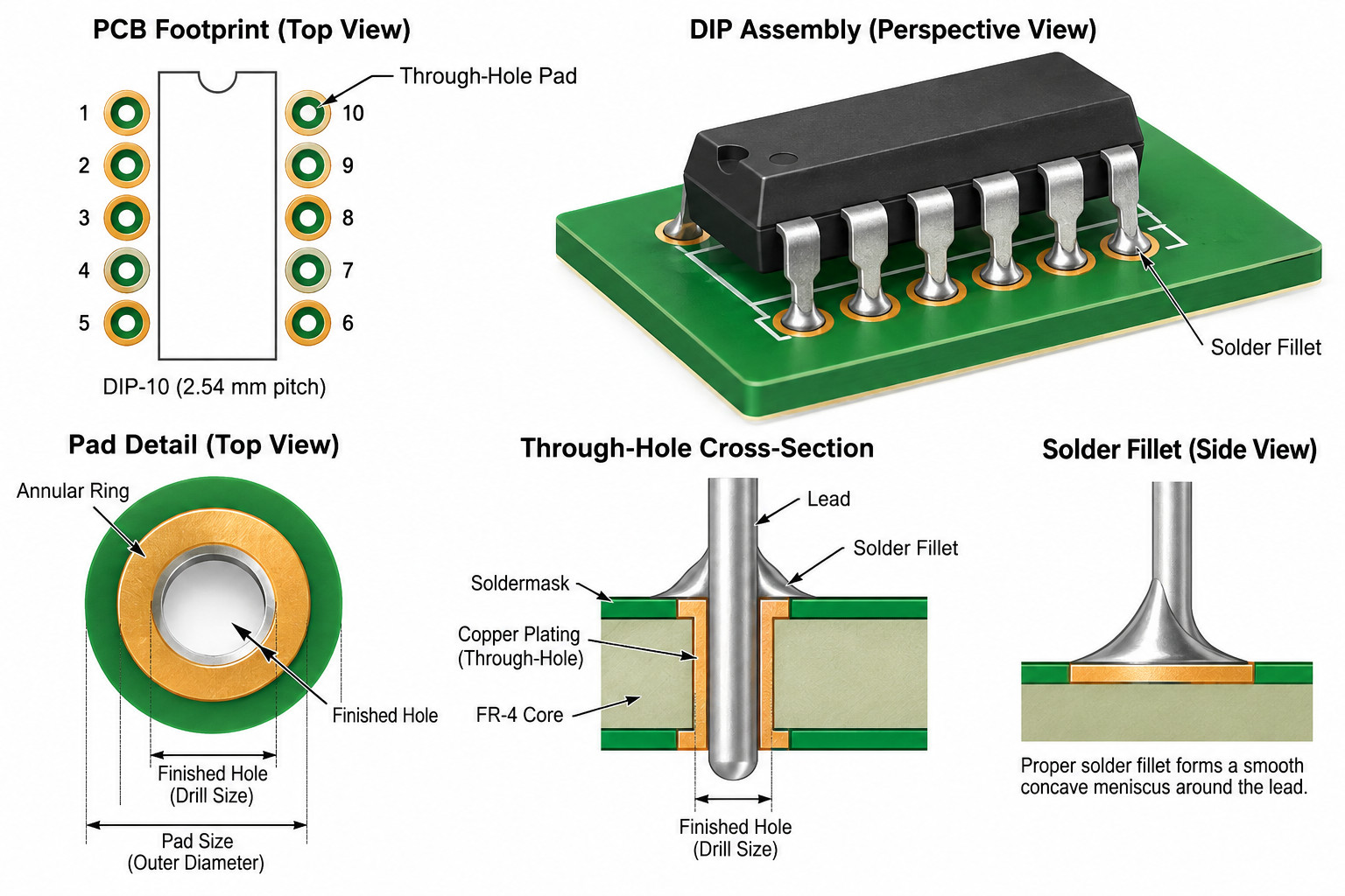
A feed-through via is a plated electrical connection between PCB layers. A component hole receives a physical lead or pin. The difference is easiest to see around a through-hole connector: its pins enter the component holes, while nearby vias connect tracks or ground areas to another copper layer.

Hole typeWhat occupies the hole?What determines its design?
Plated viaNormally no component leadInterlayer routing, plating and electrical requirements
Plated component holeA component lead or connector pinThe component's pin dimensions and attachment method
Non-plated mounting holeA screw, locating feature or empty clearanceMechanical fit and positioning

For a soldered connector pin, the finished hole must accommodate the lead and the intended solder joint. A via has no inserted pin to accommodate, so its dimensions serve the routing and electrical requirements instead. Selecting one hole size for both jobs can therefore compromise connector fit or waste routing space.

On a through-hole circuit board, the manufacturing drawing therefore needs to distinguish component holes, vias and mechanical holes. This prevents a connector's mounting requirements from being mistaken for ordinary routing-hole dimensions.

PCB feed-through card

What does a feed through connector do?

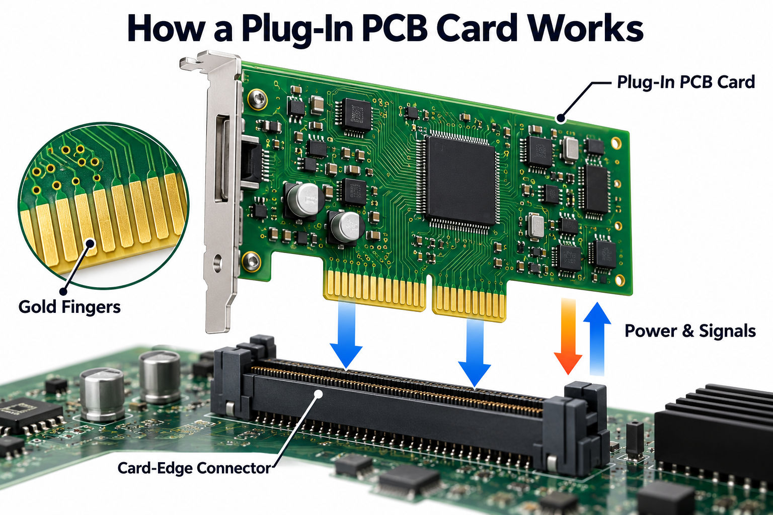
A feed through connector carries an electrical connection across a physical boundary, such as an enclosure wall. It provides a defined point where external wiring meets the equipment inside. Depending on the design, the internal side connects to another cable, terminals or a PCB.

The connector and the PCB solve different parts of the connection. The connector establishes the mating interface; the PCB routes those contacts onward. A panel-mounted feed-through may be supported by the enclosure, while a board-mounted connector depends on its PCB attachment and any additional mechanical supports. The mounting arrangement determines where mating forces are carried.

For a replacement, pin pitch alone is insufficient. Two connectors with the same spacing can have different keying, contact numbering or mating depths. An apparently matching plug can therefore connect the wrong circuits or fail to engage correctly.

An ordinary conductive feed-through passes the intended electrical connection continuously. Insulation separates adjacent contacts or separates them from the housing; galvanic isolation requires a different circuit arrangement. Filtering and sealing are additional functions of specified products, not inherent properties of every feed-through connector.

When are feed through capacitors needed?

Feed through capacitors are useful when high-frequency noise must be reduced along a power or suitable signal path. In a three-terminal feed-through arrangement, current passes through the component's conductive path, while its capacitance provides a path for noise to ground. The low-inductance structure helps it remain effective at frequencies where a conventional capacitor's parasitic inductance limits suppression.

Choose the connection according to the problem being solved:

  • Noise travelling along a power line: A through connection places the filter in that route. The supply trace is interrupted so that current flows through the component's input and output terminals.
  • Local IC supply-voltage fluctuations: A non-through connection uses the component for bypass decoupling while retaining the main supply trace. Because noise can also continue along that trace, it offers less suppression of escaping noise than the through arrangement.
  • A line carrying useful signals: The filter must pass the required signal spectrum. If unwanted noise lies close to useful signal frequencies, indiscriminately adding capacitance can suppress signal harmonics as well as noise. The filter response must suit both.

For a power-line through connection, first eliminate parts that cannot meet the operating voltage and current. Then compare attenuation over the troublesome frequency range and the voltage drop caused by the component's DC resistance.

A simple voltage-drop example: If a candidate filter has 20 mΩ of DC resistance and carries 2 A, its calculated drop is 40 mV:

Voltage drop = current × resistance = 2 A × 0.020 Ω = 0.040 V.

That is an illustrative calculation, not a rating for a particular product. It shows why a filter can have suitable noise performance yet consume too much of a low-voltage rail's available voltage margin. Select for both electrical delivery and noise suppression.

How do PCB layout and grounding affect feed-through filters?

The filter's ground connection is part of the noise-current path. A long, narrow route to ground adds inductance, making that path harder for high-frequency current to follow. Consequently, the same filter can produce different attenuation on two boards.

Three layout choices have a direct effect:

  • Ground-trace length and width: Short, wide connections reduce the inductance added between the filter's ground pads and the grounding structure.
  • Distance to the ground plane: A via reaching a nearby plane has a shorter connection than one reaching a plane near the opposite board surface. Stackup matters even when the top-view layout looks identical.
  • Ground connections at the component: In a multilayer mounting comparison, connecting both ground sides through vias gave greater attenuation than using a single ground-side via; shorter vias also improved performance. These are results for that arrangement, not a universal via-count rule.

Keep the incoming and outgoing routing distinct around the filter as well. Closely coupled input and output structures can allow some high-frequency noise to couple around the component. Both the through/non-through choice and this input/output routing effect determine whether noise actually follows the intended filtering path.

For a multilayer PCB, the practical priority is to establish the ground-plane position and the filter's connection paths together. Changing the ground-layer depth during a board revision can change filtering behavior even if the component and its surface footprint remain unchanged.

What must match when replacing a feed-through card?

A successful replacement preserves how the card connects, fits and behaves in the equipment. Three differences are especially easy to miss when comparing boards by appearance.

Pin mapping can change without changing the connector outline.

Imagine two boards using the same six-position connector. On one, contact 1 carries supply power; on the other, it carries ground. The plug may fit both perfectly, but the boards are electrically incompatible. Connector orientation and contact numbering must therefore be interpreted from the specified viewing direction, not guessed from a photograph.

A filtered connection can look like a simple pass-through.

Replacing a filter with a copper link preserves DC continuity but removes its intended noise suppression. Even a capacitor with the same nominal capacitance may differ in internal construction, resistance or high-frequency response. A replacement should preserve the relevant electrical characteristics, not merely the marking value.

Mechanical fit includes the assembled components.

A board can match the original outline yet place a connector too high, reverse its mating direction or leave insufficient clearance inside the enclosure. Board thickness, mounting-hole positions and connector location need to work as one assembly.

The original assembly part number and revision provide a useful starting point for these comparisons. When reproducing an obsolete board, concentrate first on its connection map, populated components and assembled geometry. Resolve those differences before treating a similar-looking board as interchangeable.

PCB feed-through card

FAQs About PCB feed-through card

Is a multilayer PCB required for a feed-through card?

No. A simple connection board may use a simpler layer structure. Additional layers become useful when routing density, grounding or signal requirements justify them. The term “feed-through” does not specify a layer count.

Can one card combine through-hole connectors and surface-mount filters?

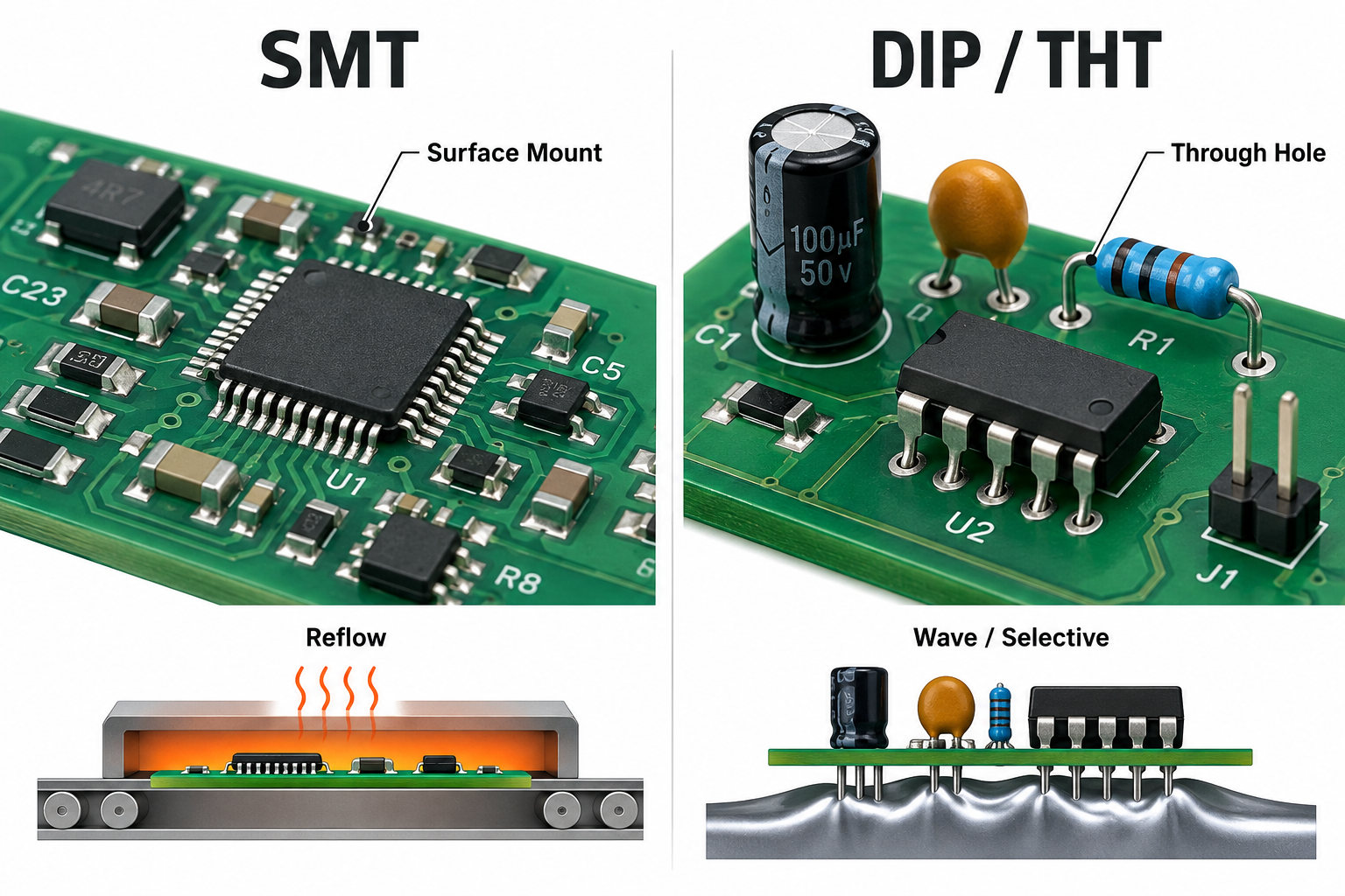
Yes. Connector pins and small filter components can use different mounting methods on the same board. This calls for mixed assembly rather than treating the whole card as exclusively SMT or through-hole.

Will a continuity test verify the card's filtering performance?

No. Continuity checks whether a conductive path exists. Filtering concerns how the circuit behaves across frequency, so it requires a measurement suited to the noise or signal requirement. Both checks can be useful, but they answer different questions.

Can I supply the connectors for a custom build?

Yes. EBest Circuit supports consignment and partial turnkey assembly, allowing you to supply specified components while we arrange the agreed remaining procurement and assembly. This is useful when a connector must match existing equipment or cable assemblies.

Should I order a bare PCB or an assembled card?

Order a bare PCB when you will install the connectors and other components yourself. Order an assembled card when you need those components fitted. A bare board reproduces the copper and hole structure; the populated components complete the specified circuit.

Planning a custom PCB feed-through card for your equipment? EBest Circuit can manufacture the board and assemble its specified connectors and components, including mixed SMT and through-hole builds. Email sales@bestpcbs.com to discuss turning your board design into an assembled unit ready for your equipment trials.

You may also like

PCB and PCBA manufacturer USA: Compare Your Options

September 10th, 2026

For a PCB and PCBA manufacturer USA buyers can work with directly, options include Sierra Circuits, Gorilla Circuits, and Cirexx. These companies offer domestic fabrication and assembly, with services covering standard FR4 prototypes, complex multilayer boards, and specialized constructions. Small-order availability and HDI capability help distinguish the services within that market.

For projects that allow overseas production, EBest Circuit (Best Technology) combines PCB manufacturing, component sourcing, and assembly in China. Our capabilities include FR4 boards up to 32 layers and BGA assembly down to 0.25 mm pitch, supporting projects from bare-board prototypes to populated assemblies. Discuss your US project with our team at sales@bestpcbs.com, or arrange a factory visit to see our manufacturing operations firsthand.

PCB and PCBA manufacturer USA

US PCB Manufacturers Offering Fabrication and Assembly

Sierra Circuits, Gorilla Circuits, and Cirexx each provide both PCB fabrication and assembly. Their service ranges cover different board technologies and production needs.

Manufacturer PCB manufacturing Assembly services
Sierra Circuits Standard rigid FR4 and custom advanced boards, including HDI In-house assembly and component procurement
Gorilla Circuits Multilayer boards, hybrid constructions, and semiconductor test boards In-house assembly, parts procurement, and testing options
Cirexx Rigid, flex, rigid-flex, HDI, and RF/microwave boards Turnkey, partial turnkey, and consignment assembly

Sierra Circuits offers a defined route for conventional prototypes through Turnkey PRO, which combines rigid-board fabrication, parts, and assembly. More complex constructions use its custom services.

Gorilla Circuits fabricates and assembles boards at its San Jose, California campus. Its semiconductor test work includes final-test and probe-card boards, making this a relevant area of experience for buyers sourcing complex test hardware.

Cirexx combines fabrication and assembly within the same facility. Flex and rigid-flex assembly are particular areas of specialization, alongside rigid-board and HDI work.

Do All PCB Manufacturers Offer Assembly?

No. A PCB fabrication order normally supplies bare boards; assembly adds the components. Some manufacturers provide both services, while others specialize in one stage.

  • PCB fabrication: bare boards ready for component assembly.
  • Consignment assembly: assembled boards using customer-supplied materials.
  • Full turnkey PCB assembly: fabrication, component purchasing, and assembly managed by the supplier.

An assembler can also purchase bare boards from a fabrication partner. Consequently, turnkey service does not necessarily mean both processes happen in the same factory.

If you already have an assembly partner, a specialist bare-board manufacturer may fit your project well. If you need finished assemblies and want one point of coordination, a fabrication-and-assembly provider can handle the transition between the two stages.

US Manufacturing vs. Overseas Supply to the USA

US production offers proximity; overseas production broadens the manufacturing options available to US buyers. The balance changes with the way a project is developed and ordered.

Consideration US manufacturing Overseas supply to the USA
Factory access Easier domestic visits and sample exchanges Visits require international travel
Engineering communication Greater overlap with US working hours Responses span different working hours
Shipping Domestic transport to the customer International transit before US delivery
Repeat orders Convenient for closely coordinated local production Can suit scheduled orders with planned shipping

During active development, proximity can be valuable. A team making frequent revisions may benefit from easier sample exchanges and direct factory interaction. The relevant schedule is the complete cycle from placing a build to evaluating the hardware.

For a stable design, manufacturing fit becomes more prominent. Materials, copper construction, component availability, and the supplier's ability to repeat the build can matter more than how often the team can visit. Overseas production is worth considering when international transport fits that schedule.

Neither location guarantees a lower total price. Compare equivalent finished boards: the same materials, components, assembly scope, and delivery destination. A bare-board quotation and a complete PCBA quotation cover different purchases.

Which US PCB and PCBA Manufacturers Accept Small Orders?

Sierra Circuits, Cirexx, and PCB Unlimited offer services for prototype or low-volume assembly. Their small-order arrangements differ:

Provider Small-order service Relevant option
Sierra Circuits Turnkey PRO: generally 2–100 assembled boards, depending on the design Standard rigid FR4 turnkey builds
Cirexx High-mix, low-quantity assembly; prototype through medium volume Custom rigid, flex, and rigid-flex projects
PCB Unlimited USA assembly service with no minimum order quantity Turnkey or customer-supplied-material assembly

PCB Unlimited offers US assembly services. Sierra and Cirexx also provide in-house board fabrication. For Sierra, confirm availability before planning a one-board assembled order.

A small quantity can still involve a custom board. A five-board rigid-flex project or a four-layer PCB with a specified stackup may need a custom service rather than a standard prototype package.

Small runs also share production preparation across fewer finished boards. Stencil preparation and machine programming are needed even for a short run, so doubling the assembled quantity does not necessarily double the total price. When several engineers need hardware simultaneously, pricing the actual number of working samples can be more useful than starting with the smallest possible order.

PCB and PCBA manufacturer USA

Which US Manufacturers Offer HDI PCB Fabrication and Assembly?

Sierra Circuits and Cirexx offer both HDI fabrication and assembly. Their capabilities include the board interconnections and component assembly needed for dense designs.

Manufacturer HDI fabrication Assembly support
Sierra Circuits Custom HDI boards with advanced via structures Turnkey HDI assembly with component sourcing
Cirexx Laser-drilled microvias, blind/buried vias, sequential lamination, and via-in-pad Double-sided HDI SMT/BGA assembly

Sierra's HDI projects use its custom manufacturing route. The standard Turnkey PRO package excludes HDI and multiple laminations, so it is a separate service from the company's advanced-board offering.

Cirexx combines HDI fabrication with dense assembly work. Its fabrication processes include laser direct imaging and controlled-depth drilling, while its assembly service covers double-sided SMT/BGA builds and flex or rigid-flex boards.

For a compact BGA board, this combination is important: the fine-pitch package must be supported by a manufacturable routing and via structure beneath it. Choosing a supplier that handles both allows those fabrication and assembly requirements to be addressed together.

PCB and PCBA manufacturer USA

How EBest Circuit Supports US PCB and PCBA Buyers

With EBest Circuit, US customers can source bare PCBs, populated boards, or a complete turnkey build through one manufacturing partner. Our PCB manufacturing capabilities cover conventional FR4 and more demanding multilayer constructions.

Capability EBest Circuit support
FR4 layer count Up to 32 layers
HDI trace width/spacing Down to 2/2 mil
Small-component assembly Down to 01005
BGA assembly Down to 0.25 mm pitch
Assembly methods SMT, through-hole, and mixed assembly

The applicable combination depends on the board construction and component layout.

Keep component purchasing flexible. Our PCB assembly services include full turnkey, partial turnkey, and consignment work. You can use components already held by your team while we source the remaining parts, or have procurement included with the build.

Combine fine-pitch assembly with solder-joint inspection. Fine-pitch placement supports compact layouts, while AOI and X-ray inspection provide complementary checks for visible features and hidden solder joints.

Plan prototype and repeat builds with clear timing. Standard PCBA service is approximately one week, with expedited options for eligible projects. Our production lead times distinguish PCB fabrication from assembly; component procurement and delivery to the USA also need to fit the overall schedule.

Case Study: A 4-Layer Medical PCB for a US Customer

EBest Circuit worked with a US customer on a four-layer FR4 PCB for a medical product. The project required TG170 material, a finished thickness of 1.6764 mm ±10%, and 2 oz finished copper on every layer. The customer's PDF defined the layer structure.

Three requirements gave this board its specific manufacturing character:

  • The same finished copper requirement on all four layers. Both inner and outer layers required 2 oz copper. An outer-layer-only 2 oz specification would not describe this board correctly, and the customer's stackup formed part of the required construction.
  • Copper retention around non-plated holes. Where a pad was larger than an NPTH, the customer required its position and copper to remain unchanged. Secondary drilling was specified to produce the hole without treating the surrounding pad copper as material to remove.
  • A defined PTH copper requirement. Minimum hole-wall copper had to follow IPC-6012 Class 3 requirements. This was a distinct requirement from the 2 oz finished copper specified for the circuit layers.

The board also required lead-free HASL, glossy green solder mask on the top side, and white silkscreen clear of the pads. Routed internal corners had to follow the maximum radii on the drawing.

FAQs About PCB and PCBA manufacturer USA

Can a US assembly company work with overseas-manufactured PCBs?

Yes, if it accepts customer-supplied boards or sources them through a fabrication partner. This arrangement lets you retain a bare-board supplier while assembling closer to your US team.

Can prototype orders use a custom stackup?

Yes. Small quantity and custom construction can be combined. The order needs a service that accepts the specified stackup rather than a package limited to the supplier's standard constructions.

Can I provide some components and have the supplier purchase the rest?

Yes. Partial turnkey assembly supports this arrangement. It is useful when you already hold selected devices but want the manufacturer to procure the remaining components.

Does PCB electrical testing replace PCBA functional testing?

No. Bare-board electrical testing checks circuit connectivity before assembly. Functional testing evaluates the populated board against its intended functions and requires an appropriate test method.

Can EBest Circuit support a US project from bare boards through assembly?

Yes. EBest Circuit provides PCB fabrication, component sourcing, and assembly in China for US customers. The project can be supplied as bare boards or developed into a turnkey assembly order.

Discuss your next PCB or PCBA project with EBest Circuit at sales@bestpcbs.com. If you would like to meet the team and see our production operations before choosing a manufacturing partner, we welcome you to arrange a factory visit. PCB and PCBA manufacturer USA

You may also like

Cleaning Electronics With Rubbing Alcohol: 70%, 90%, or 99% IPA?

September 10th, 2026

Cleaning electronics with rubbing alcohol can be safe when the device is disconnected from power, the liquid is kept out of openings, and the concentration matches the surface. For exposed PCBs, 90% to 99% electronics-grade isopropyl alcohol (IPA) is usually a better starting point than 70% rubbing alcohol because it contains less water and dries faster.

That does not make IPA a universal electronics cleaner. Display coatings, printed legends, adhesives, unsealed sensors, and some plastics may be damaged. The contamination also matters: IPA can lift oils and many rosin-based flux residues, but it may not remove salts, sugary spills, water-soluble flux, or cured residues.

Technician cleaning a powered-off PCB at an ESD-safe workbench with rubbing alcohol

Can You Clean Electronics With Rubbing Alcohol?

Yes, you can clean selected electronics with rubbing alcohol after removing power and confirming that the device maker permits alcohol on the target surface. A slightly damp lint-free cloth may be suitable for an approved hard exterior, while an exposed PCB normally calls for controlled application of 90% to 99% electronics-grade IPA.

First decide which job you are doing:

  • Exterior wiping: Some manufacturers permit 70% IPA wipes on hard, nonporous surfaces. Apple and Dell publish product-specific examples, but their instructions do not apply automatically to every device.
  • Exposed-board cleaning: Repair guides commonly use at least 90% IPA for localized work on a disconnected logic board or PCB.
  • Disinfection: The concentration and wet contact time needed to disinfect a surface are different from the requirements for removing flux or oil from a circuit board.

Never spray alcohol directly onto a device. Wet the cloth, foam swab, polyester swab, or ESD-safe brush away from the electronics, then apply only enough liquid to loosen the soil.

Is Rubbing Alcohol Safe for Electronics?

Rubbing alcohol is safe only for compatible materials and controlled, unpowered cleaning; it is not safe to pour into an assembled device or use around ignition sources. A 70% IPA wipe may be approved for a laptop shell or keyboard, yet the same liquid can enter a connector, remain beneath a shield, soften adhesive, or mark a coated display.

This is why the answer to whether rubbing alcohol is safe for electronics depends on the exact part, contamination, and application method rather than the device category alone.

The label matters as much as the percentage. A bottle sold as first-aid rubbing alcohol is formulated for topical use, not residue-sensitive PCB production. Many 70% products contain 30% water, and formulations vary by supplier. Before use, check the active ingredients, inactive ingredients, and safety data rather than assuming every clear alcohol product is equivalent.

IPA is also highly flammable. NIOSH lists isopropyl alcohol as a Class IB flammable liquid with a 53°F (12°C) flash point. Keep it away from soldering irons, hot-air rework tools, sparks, smoking, and open flame; cap the container when not in use and provide ventilation.

What Percentage Isopropyl Alcohol for Electronics?

Use the device maker’s approved product for finished equipment; for localized exposed-PCB cleaning, 90% to 99% electronics-grade IPA is the practical starting range because it contains only 1% to 10% water instead of the 30% found in 70% IPA. Higher purity does not override component, coating, or adhesive restrictions.

IPA Concentration Approximate Water Content Suitable Starting Use Main Limitation
70% 30% Approved hard exterior surfaces using a damp wipe Slower drying and more water; not the default for exposed PCBs
90% or 91% 9% to 10% Localized PCB repair and residue removal when compatible Can still affect coatings, plastics, markings, and adhesives
99% or 99.9% 0.1% to 1% Moisture-sensitive, residue-controlled bench cleaning Still flammable and not effective against every contaminant
Comparison of 70 percent, 90 percent, and 99 percent IPA for exterior and exposed PCB cleaning

Do not dilute high-purity IPA with tap water for PCB work. Tap water can add minerals and ions. If an aqueous process is required, it should use chemistry, rinse-water quality, and drying conditions chosen for the assembly.

What Is the Difference Between Rubbing Alcohol and Electronics-Grade IPA?

Household rubbing alcohol is usually sold as a skin antiseptic, whereas electronics-grade IPA is supplied with controlled purity and residue expectations for cleaning components and assemblies. A common 70% first-aid product is 70 mL IPA per 100 mL with water as the inactive ingredient; an electronics cleaner may be 99.9% anhydrous IPA with a technical data sheet and safety data sheet.

Do not judge a cleaner by the front label alone. Check:

  • IPA concentration and water content;
  • listed fragrance, dye, oil, bitterant, or other additive;
  • nonvolatile residue specification, if provided;
  • plastics, elastomer, coating, and adhesive compatibility;
  • storage, ventilation, and personal-protection instructions in the SDS.

For a repeatable manufacturing process, lot-controlled cleaner and documented compatibility are more useful than a generic pharmacy bottle whose intended use is first aid.

Which Parts Should Not Be Cleaned With Rubbing Alcohol?

Do not apply rubbing alcohol to an unapproved display coating, printed key legend, foam adhesive, acrylic or polycarbonate part, unsealed microphone, speaker, sensor, relay, or coated PCB area without a material check. Even when the bare laminate and solder mask tolerate IPA, a complete assembly may contain liquid-trapping or solvent-sensitive parts.

Display coating, printed legends, adhesive tape, and an unsealed sensor that require IPA compatibility checks
  • Displays and lenses: Alcohol can affect oleophobic, anti-glare, or other surface treatments unless the manufacturer permits it.
  • Printed markings: Repeated wiping can fade legends on keys, component bodies, labels, and enclosures.
  • Adhesives and foam: IPA is often used to weaken adhesive during repair, which is exactly why it must be controlled near display seals, battery tape, gaskets, and foam pads.
  • Liquid-sensitive devices: Microphones, speakers, MEMS parts, unsealed switches, relays, transformers, and trimmers can trap solvent or suffer mechanical damage.
  • Conformal coating: Cleaning a coated board and intentionally removing coating are different processes. Review the coating chemistry before applying solvent.

How Should You Prepare Electronics Before Cleaning?

Shut the device down, unplug every cable, remove the battery when serviceable, verify stored energy is discharged, and move the work away from sparks, hot tools, and open flame. A power button does not isolate every energy source, and power supplies or large capacitors may retain hazardous voltage after unplugging.

  1. Read the product cleaning or service instructions.
  2. Photograph connectors, cable routing, corrosion, and residue before disassembly.
  3. Disconnect mains power, external supplies, and batteries.
  4. Use an ESD-safe mat, grounded tools, and an ESD-safe brush for sensitive boards.
  5. Remove loose dust first so wet cleaning does not turn it into a paste.
  6. Test the cleaner on a hidden or representative material when compatibility is uncertain.
  7. Use ventilation and keep the IPA container away from ignition sources.

If you cannot safely discharge the equipment, access the board without damaging seals, or identify a swollen battery, stop and use a qualified repair service.

How Do You Clean an Exposed PCB With Isopropyl Alcohol?

Apply a small amount of 90% to 99% electronics-grade IPA to a low-lint swab or ESD-safe brush, loosen the soil, then lift the dissolved residue with clean material instead of letting dirty solvent dry on the board. The goal is removal, not simply spreading a dissolved film across a larger area.

Controlled cleaning of flux residue from an exposed PCB with a low-lint swab
  1. Inspect and classify the soil. Note whether it is dry dust, oil, flux, drink residue, corrosion, or an unknown deposit.
  2. Remove dry particles. Use an ESD-safe soft brush or controlled clean air without forcing debris under packages.
  3. Dampen the tool. Add IPA to the swab or brush away from the PCB; do not pour from the bottle onto the board.
  4. Agitate gently. Work around solder joints and leads without bending parts or snagging fine wires.
  5. Lift the dissolved residue. Blot with a clean low-lint wipe or use fresh solvent as a controlled final rinse.
  6. Replace dirty materials. A brown swab or cloudy solvent is carrying contamination and should not be reused for the final pass.
  7. Dry, inspect, and test. Confirm that connectors, shields, sockets, and package gaps are dry before reconnecting power.

For a broader method covering dust, corrosion, coating, and aqueous cleaning, see our guide to cleaning a PCB board safely.

Which Contaminants Need More Than IPA?

Salt, sugary drinks, water-soluble flux, corrosion products, and unknown deposits may require a qualified aqueous rinse, flux-specific cleaner, or repair process rather than an IPA-only wipe. IPA can evaporate while nonvolatile ionic contamination stays behind.

Contaminant Suitable Starting Method Why IPA Alone May Fail
Finger oil or light grease Compatible high-purity IPA and clean low-lint material Dirty solvent can redeposit an oily film
Rosin-based flux High-purity IPA or matched flux remover after compatibility check Heat-aged or polymerized residue may resist IPA
Water-soluble flux Validated aqueous chemistry and DI-water rinse IPA may not remove the ionic activator system
Sugary or salty spill Controlled aqueous cleaning, DI rinse, and complete drying when parts allow Alcohol can leave conductive nonvolatile material behind
Corrosion Cleaning plus magnified damage assessment and repair Solvent cannot restore missing copper or damaged terminations

Flux chemistry should be identified before selecting the cleaner. Our explanation of flux residue and cleaning methods shows why water-soluble, rosin, and no-clean materials cannot share one blanket instruction.

In our PCBA projects, we treat cleaner selection, rinse quality, drying, and inspection as one process. Changing only the solvent can leave the same ionic residue or hidden moisture problem in a different form.

How Long Should Electronics Dry Before Power-On?

Do not use one universal minute count; restore power only after visible liquid and alcohol odor are gone and no fluid remains trapped under shields, connectors, sockets, switches, or packages. A lightly wiped open surface may appear dry within minutes, while a flooded connector or shielded area can retain solvent much longer.

Use these release checks:

  • no droplets, wet sheen, or cleaner line visible under magnification;
  • no liquid emerging when the board is tilted or gently repositioned;
  • connectors and sockets inspected from more than one angle;
  • no alcohol odor at close range in a ventilated area;
  • no residue film, displaced component, lifted pad, or damaged marking;
  • the device maker’s minimum drying instruction has been met.

Do not use a hot heat gun to accelerate drying. Excessive heat can deform connectors, soften adhesives, damage batteries, or stress solder joints. Use clean dry air or a controlled low-temperature process only when the component limits are known.

What Mistakes Damage Electronics During Alcohol Cleaning?

The highest-risk mistakes are cleaning an energized device, spraying directly into openings, flooding liquid-sensitive parts, using a contaminated swab, and restoring power before trapped solvent has evaporated. Most failures come from uncontrolled application or wrong-material use, not from the word “alcohol” alone.

  • Using 70% as the universal choice: It may be suitable for an approved exterior but adds more water to an exposed assembly.
  • Using a soaked cotton swab: Excess liquid can wick under components, and loose fibers can snag on leads.
  • Letting dirty IPA evaporate: Dissolved flux and oil remain unless they are lifted or rinsed away.
  • Scrubbing harder: Force can remove markings, dislodge 0201/01005 components, bend contacts, or break corroded leads.
  • Ignoring the original fault: Cleaning cannot repair a cracked joint, missing copper, swollen battery, or internally corroded component.
  • Applying conformal coating over residue: Cleanliness and dryness must be verified before coating, or contamination may be sealed onto the assembly.

Production control begins earlier than final cleaning. For example, solder paste inspection in PCB assembly can catch printing defects before placement and reflow, while post-solder cleaning addresses only the residue left by the selected materials and process.

FAQ About Cleaning Electronics With Rubbing Alcohol

These answers cover the most common concentration, surface, flux, and power-on questions about using rubbing alcohol on electronics.

Can I use 70% rubbing alcohol on a circuit board?

Use 70% rubbing alcohol on an exposed circuit board only when the assembly documentation permits it and no better high-purity option is available. Its 30% water content slows drying and raises the chance of liquid remaining in gaps. For localized exposed-PCB cleaning, 90% to 99% electronics-grade IPA is usually the safer starting range.

Is 91% rubbing alcohol good for electronics?

91% IPA is suitable for many localized PCB-repair tasks because it contains about 9% water and evaporates faster than 70%. It can still soften adhesive, affect markings, or enter unsealed parts, so apply a small amount to a low-lint tool and check material compatibility first.

Can I use 99% isopropyl alcohol on a phone screen?

Do not use 99% IPA on a phone screen unless the phone manufacturer explicitly approves it for that model and surface. Screen coatings and display seals vary. Many device makers specify a slightly damp lint-free cloth or a 70% IPA wipe for selected exterior surfaces, not unrestricted use of 99% liquid.

Does isopropyl alcohol remove solder flux?

IPA removes many fresh rosin-based flux residues, especially at 91% to 99%, but it does not remove every no-clean or heat-aged residue. Water-soluble flux normally requires a validated aqueous process. Match the cleaner to the exact flux product and remove the dissolved soil rather than letting it dry on the PCB.

Can cleaning electronics with alcohol cause a short circuit?

Cleaning electronics with alcohol can cause a short circuit if power is present, the liquid contains conductive contamination, or water and dissolved residue remain trapped when the device is energized. Disconnect every power source, control the liquid, dry hidden areas, inspect the board, and only then perform a safe functional test.

Can I pour rubbing alcohol over a motherboard?

Do not pour household rubbing alcohol over an assembled motherboard. Flooding carries dirt beneath packages and into connectors, fans, sockets, microphones, switches, or other liquid-sensitive parts. Board immersion is a specialized repair process that requires disassembly, compatible components, suitable high-purity solvent, ventilation, and controlled drying.

How Can EBest Circuit Support Cleaner, More Reliable PCB Assemblies?

We match the cleaning method to the flux, component set, coating plan, inspection requirement, and end-use risk instead of treating IPA as a universal production solution. At EBest Circuit, we support PCB fabrication, component sourcing, PCB assembly, and inspection within one coordinated project.

For a cleaning-sensitive assembly, send us the Gerber files, BOM, placement data, assembly drawing, target flux or solder-paste specification, coating requirement, quantity, and cleanliness or test criteria. We can review the build information before production and align the inspection plan with the assembly design.

To discuss a PCB or PCBA project, visit our PCB and PCBA manufacturing service page or email sales@bestpcbs.com.
You may also like

What Does Solder Flux Do? How It Works in Electronics Soldering

September 9th, 2026

What does solder flux do? Solder flux removes surface oxides, limits new oxidation during heating, and helps molten solder wet copper pads, component leads, wires, and terminals. Without enough flux activity, solder may bead up or pull away from the metal instead of forming a clean joint.

In electronics soldering, flux may come from flux-core wire, solder paste, liquid flux, or tacky flux used during rework. The chemistry varies by process, but the purpose is the same: keep the soldering surface clean enough for solder to spread and bond while the joint is hot.

What solder flux does during electronics soldering on a PCB

What Does Solder Flux Actually Do?

Solder flux mainly cleans and protects the metal surface so molten solder can wet it properly.

Its main functions are:

  • Remove oxides: Activators react with oxide films on copper pads and component terminals.
  • Limit re-oxidation: Flux temporarily protects hot metal from further exposure to oxygen.
  • Improve wetting: Molten solder can spread across clean metal instead of remaining in rounded beads.
  • Support joint formation: Better wetting helps solder make continuous contact with both surfaces being joined.

This is why adding suitable flux can improve a stubborn solder joint even when the soldering temperature is already high enough.

Flux itself is not an adhesive. It prepares the surface so solder can form the actual electrical and mechanical connection.

How Does Solder Flux Work During Soldering?

Solder flux works by becoming chemically active as the joint heats up, removing surface oxides before molten solder reaches the metal.

Five-step diagram showing how solder flux removes oxide and improves solder wetting

A typical sequence is:

  1. Copper pads or component leads have a thin oxide layer.
  2. Flux is applied or released from solder wire or solder paste.
  3. Heat activates the flux.
  4. Flux chemistry reacts with the oxide layer.
  5. Cleaner metal is exposed.
  6. Molten solder wets and spreads across the surface.
  7. The solder cools and forms the joint.

The most important result is better wetting.

Good wetting produces smooth contact between the solder and the metal surface. Poor wetting can leave:

  • rounded solder beads
  • incomplete pad coverage
  • uneven fillets
  • solder that pulls away from the pad or lead

Increasing iron temperature alone does not fix an oxide problem. Excessive heat can accelerate oxidation while also increasing the risk of pad damage or component stress.

Do You Need Flux to Solder?

Yes, most soldering processes need flux activity, but you do not always need to apply flux separately.

Flux-core wire, solder paste, and extra flux used for PCB rework

Flux may already be present in:

  • flux-core solder wire
  • SMT solder paste
  • some solder preforms
  • certain specialty solder products

Extra flux is more useful when the existing flux is no longer sufficient, such as during:

  • PCB rework
  • repeated heating of an old solder joint
  • soldering oxidized pads or leads
  • drag soldering
  • fine-pitch IC soldering
  • BGA or QFN rework

So, if you are using flux-core solder or solder paste, the process already includes flux. Separate flux is only needed when additional oxide removal or wetting support is required.

In production PCBA, flux choice is more than a soldering consumable decision. It can affect solder wetting, residue control, ionic cleanliness, conformal coating compatibility, inspection results, and long-term reliability. For SMT, wave soldering, selective soldering, or rework projects, EBest Circuit can review flux and soldering process requirements together with the PCB design, BOM, and assembly conditions.

Does Solder Already Have Flux in It?

Some solder contains flux, while other solder products do not.

Comparison of solid solder wire, flux-core solder wire, solder paste, and solder bar
Solder Material Contains Flux? Typical Use
Solid solder wire No Controlled or specialized soldering
Flux-core solder wire Yes Hand soldering and repair
SMT solder paste Yes Reflow assembly
Solder bar Usually no Wave and selective soldering
Solder preform Depends on product Specialized assembly

Flux-core solder wire is common in manual electronics soldering. When the wire melts, the internal flux is released directly into the joint.

Solder paste also contains flux, but in a different form. It combines fine solder alloy powder with a flux system designed for stencil printing and reflow.

Extra flux may still help when:

  • the original flux has already been consumed
  • the joint has been reheated several times
  • the surface is oxidized
  • additional wetting is needed around fine-pitch leads

What Does Solder Flux Contain?

Solder flux usually contains a base material, activators, and a carrier or solvent.

The main ingredients are:

  • Base or resin: Often rosin or synthetic resin. It provides the main flux medium.
  • Activators: React with metal oxides during heating.
  • Solvent or carrier: Helps liquid flux spread and evaporates as the assembly heats.

Depending on the product, manufacturers may also add:

  • wetting agents
  • corrosion inhibitors
  • stabilizers
  • rheology modifiers
  • thixotropic agents

The exact formulation affects flux activity, residue, storage stability, application method, and cleaning requirements.

What Types of Flux Are Used in Electronics Soldering?

The main flux types used in electronics are rosin-based, no-clean, and water-soluble flux.

Rosin RMA, no-clean, and water-soluble flux types used in electronics soldering
Flux Type Activity Cleaning Typical Use
Rosin / RMA Low to medium Depends on formulation Hand soldering, repair
No-clean Low to medium Often not required SMT, reflow, wave soldering
Water-soluble Medium to high Normally required More difficult solderability conditions

Rosin and RMA flux

Rosin flux is widely used in electronics. RMA, or mildly activated rosin, adds more oxide-removal capability while remaining suitable for many PCB applications.

No-clean flux

No-clean flux leaves a relatively small amount of residue after soldering and is common in production assembly.

The term “no-clean” does not mean the board is residue-free. It means the remaining residue is designed to stay on the board when the process and product requirements allow it.

Water-soluble flux

Water-soluble flux offers higher activity and can handle more difficult oxidation. Its residues normally need to be removed after soldering.

For PCB work, plumbing or highly acidic flux should not be used because the residue may be too corrosive for electronic assemblies.

Liquid Flux vs Paste Flux: What Is the Difference?

Liquid flux spreads easily, while paste or tacky flux stays in place more effectively.

Flux Form Main Characteristic Typical Use
Liquid flux Low viscosity, spreads easily Wave soldering, selective soldering, repair
Flux pen Controlled liquid application PCB touch-up
Gel / tacky flux Stays around the joint SMD, BGA and QFN rework
Paste-type flux Thick, localized application Hand soldering and rework

Liquid flux is useful when the material needs to flow into narrow spaces or across multiple leads.

Tacky and gel fluxes are more useful during rework because they remain around the component instead of immediately spreading across the board.

Flux paste is not the same as solder paste. Flux paste contains flux chemistry, while solder paste contains both solder alloy powder and flux.

Which Flux Is Best for Soldering Electronics?

The best flux for soldering electronics depends on the soldering process, surface condition, residue requirement, and cleaning method.

Application Typical Flux Choice
General PCB hand soldering Rosin/RMA or electronics-grade no-clean
Fine-pitch IC soldering Liquid or tacky flux
SMT reflow Flux system already contained in solder paste
Wave soldering Process-specific liquid flux
BGA/QFN rework Tacky or gel flux
Oxidized surfaces Higher-activity flux with suitable cleaning

Also check:

  • solder alloy compatibility
  • PCB surface finish
  • flux activity level
  • residue limits
  • cleaning capability
  • conformal coating requirements
  • product reliability requirements

A more active flux is not automatically better. Higher activity may improve oxide removal, but it can also increase cleaning requirements.

Does Flux Need to Be Cleaned After Soldering?

Flux residue should be cleaned when the chemistry or assembly requirements make residue unacceptable.

PCB flux residue cleaning guide for water-soluble, highly active, and no-clean flux

Typical guidance is:

  • Water-soluble flux: Normally clean after soldering.
  • Highly activated flux: Usually clean unless the product specification states otherwise.
  • No-clean flux: May remain if the process and reliability requirements allow it.

Cleaning deserves extra attention for:

  • high-voltage assemblies
  • high-impedance circuits
  • assemblies receiving conformal coating
  • products exposed to high humidity
  • assemblies with strict ionic cleanliness limits

Using too much flux can also leave unnecessary residue, especially during hand soldering and repair. Applying only the amount needed for proper wetting usually gives a cleaner and more repeatable result.

FAQ About Solder Flux

1. What happens if you solder without flux?

Without enough flux, surface oxides can prevent solder from wetting properly. The solder may bead up, form incomplete fillets, or fail to bond evenly to the pad or component lead.

2. Can you use too much flux when soldering?

Yes. Too much flux can leave heavy residue, spread contamination across the PCB, and increase cleaning or inspection work. Use enough to support wetting without flooding the area.

3. Does flux make solder stick better?

Yes, indirectly. Flux removes oxides and improves wetting, allowing molten solder to bond more effectively with the metal surface. Flux itself is not an adhesive.

4. Can you use plumbing flux for electronics soldering?

No. Plumbing flux can be too aggressive or corrosive for PCB assemblies. Use flux specifically formulated for electronics.

5. Why does solder bead up even when I use flux?

Common causes include severe oxidation, contamination, insufficient heat, weak or expired flux, or poor solderability of the surface finish.

6. Do you need extra flux with flux-core solder?

Not always. Flux-core solder already contains flux. Extra flux is mainly useful for rework, oxidized surfaces, fine-pitch soldering, or joints that have already been heated.

Solder flux plays a simple but important role in electronics assembly: it keeps the soldering surface clean enough for molten solder to wet and form a reliable joint.

If you are preparing a PCB or PCBA project and need support with soldering process requirements, assembly manufacturability, or production planning, send your Gerber files, BOM, and assembly requirements to sales@bestpcbs.com

You may also like

Surface Mount Resistor Guide: Sizes, Codes, Types & Values

September 9th, 2026

A surface mount resistor is a compact resistor mounted directly onto PCB pads and assembled using surface mount technology. Common packages range from tiny 01005 and 0201 parts to larger 1206, 2010, and 2512 resistors used where more power or board space is available.

Selecting the right part involves more than resistance value. Engineers also need to consider resistor type, package size, tolerance, power rating, working voltage, TCR, and markings. This guide explains the most common surface mount resistor sizes, types, codes, and values, then shows how to choose one for a PCB.

Surface mount resistor mounted on a printed circuit board

What Is a Surface Mount Resistor?

A surface mount resistor is a resistor designed to sit directly on conductive pads on the surface of a PCB. It does not use long leads passing through drilled holes like a through-hole resistor.

Other names commonly used for the same component include:

  • SMD resistor
  • chip resistor
  • surface mount chip resistor
  • SMT resistor

SMD means surface-mount device, while SMT refers to the process used to assemble surface-mount components.

A typical chip resistor contains:

  • a ceramic substrate
  • a resistive layer
  • metal terminal electrodes
  • a protective coating

During PCB assembly, solder paste is printed on the pads, the resistor is placed by pick-and-place equipment, and the joint is formed during reflow soldering.

The surface mount resistor symbol on a schematic is normally the same standard resistor symbol used for a through-hole part. Its reference designator is usually R, such as R1 or R24. Package information such as 0603 or 0805 is defined in the PCB footprint rather than the schematic symbol.

What Are the Main Surface Mount Resistor Types?

The main surface mount resistor types differ in resistive material, precision, temperature stability, current capability, and cost.

Comparison of thick film, thin film, metal strip, metal foil, wirewound and fusible surface mount resistor types
Type Main Characteristic Common Use
Thick film Cost-effective and widely available General PCB circuits
Thin film High precision and low TCR Analog and measurement circuits
Metal strip Very low resistance Current sensing
Metal foil High stability and accuracy Precision electronics
SMD wirewound Higher power and pulse capability Power circuits
Fusible Designed to open under overload Circuit protection

Thick-film resistors

These are the standard choice for many PCB designs. They cover a broad resistance range and are readily available in packages such as 0402, 0603, 0805, and 1206.

Typical uses include:

  • pull-up and pull-down networks
  • LED current limiting
  • bias circuits
  • general signal conditioning

Thin-film resistors

Thin-film parts are used when tighter tolerance and lower temperature coefficient are required. They are common in:

  • precision amplifiers
  • sensor interfaces
  • measurement circuits
  • accurate voltage dividers

Metal strip resistors

Metal strip parts are mainly used for low-resistance current sensing. Values may be measured in milliohms rather than ohms, making them useful in battery systems, power supplies, motor drives, and power converters.

The resistor type should therefore match the electrical requirement. Two resistors with the same resistance and package size can have very different tolerance, TCR, pulse capability, and stability.

What Surface Mount Resistor Sizes Are Common?

Common surface mount resistor sizes include 0201, 0402, 0603, 0805, 1206, 2010, and 2512. Smaller packages reduce PCB area, while larger packages generally offer higher power capability and easier handling.

Surface mount resistor size comparison from 0201 to 2512 packages
Imperial Size Metric Code Approx. Size (mm) Typical Conventional Power*
01005 0402 0.4 × 0.2 ~0.03 W
0201 0603 0.6 × 0.3 ~0.05 W
0402 1005 1.0 × 0.5 ~0.063 W
0603 1608 1.6 × 0.8 ~0.10 W
0805 2012 2.0 × 1.25 ~0.125 W
1206 3216 3.2 × 1.6 ~0.25 W
1210 3225 3.2 × 2.5 ~0.5 W
2010 5025 5.0 × 2.5 ~0.75 W
2512 6332 6.3 × 3.2 ~1 W

*These are common reference ratings rather than universal specifications. The exact rating must be checked in the resistor manufacturer’s datasheet.

The imperial package code approximately represents component length and width in hundredths of an inch. For example:

  • 0603 ≈ 0.06 × 0.03 inch
  • 0805 ≈ 0.08 × 0.05 inch
  • 1206 ≈ 0.12 × 0.06 inch

Metric and imperial codes should not be confused. An imperial 0603 package, for example, corresponds to metric 1608 rather than metric 0603.

Package size also affects manufacturability. Moving from 0805 or 0603 to 0402, 0201, or smaller parts generally requires tighter control of:

The smallest surface mount resistor is therefore not automatically the best choice. Use a smaller package when PCB density requires it, not simply because the package is available.

How Do You Read Surface Mount Resistor Codes and Markings?

Surface mount resistor markings use numbers and letters to represent resistance because the component body is too small for traditional color bands. The most common surface mount resistor code systems are 3-digit codes, 4-digit codes, R notation, and EIA-96.

Surface mount resistor codes and markings showing 3-digit, 4-digit, R notation and EIA-96 examples

3-digit surface mount resistor code

The first two digits are significant figures. The third digit tells you how many zeros to add.

Code Calculation Value
101 10 × 101 100 Ω
102 10 × 102 1 kΩ
103 10 × 103 10 kΩ
331 33 × 101 330 Ω
472 47 × 102 4.7 kΩ

4-digit surface mount resistor code

The first three digits are significant figures and the fourth digit is the multiplier.

Examples:

  • 1001 = 100 × 101 = 1 kΩ
  • 4701 = 470 × 101 = 4.7 kΩ
  • 1002 = 100 × 102 = 10 kΩ
  • 4702 = 470 × 102 = 47 kΩ

Four-digit markings are often found on tighter-tolerance resistor series.

R notation

For low resistance values, R is used as the decimal point.

Examples:

  • R10 = 0.10 Ω
  • R47 = 0.47 Ω
  • 2R2 = 2.2 Ω
  • 4R7 = 4.7 Ω

EIA-96 resistor markings

EIA-96 uses two digits followed by a letter. The two-digit number refers to one of 96 standard base values, while the letter gives the multiplier.

Because the number is a lookup code rather than the resistance itself, an EIA-96 surface mount resistor code chart or calculator is usually the quickest way to decode it.

Unmarked surface mount resistors

01005, 0201, and some other small resistors may have no readable top marking. Their value should be identified using:

Appearance alone is not enough because different values can use identical packages.

Surface Mount Resistor Values: What Do 100, 101, 102 and 103 Mean?

For a standard 3-digit surface mount resistor marking, the first two digits give the significant value and the third digit gives the multiplier.

Common SMD resistor code values including 100, 101, 102, 103 and 331
Surface Mount Resistor Code Resistance Value
100 10 Ω
101 100 Ω
102 1 kΩ
103 10 kΩ
221 220 Ω
331 330 Ω
472 4.7 kΩ
104 100 kΩ

The code 100 is particularly easy to misread.

100 means:

10 × 100 = 10 Ω

It does not normally mean 100 Ω.

A 100 ohm surface mount resistor commonly uses the code 101:

10 × 101 = 100 Ω

Other common examples are:

  • 102 surface mount resistor = 1 kΩ
  • 103 surface mount resistor = 10 kΩ
  • 331 surface mount resistor = 330 Ω
  • 472 surface mount resistor = 4.7 kΩ

For example, a standard 330 ohm 0805 surface mount resistor may carry the marking 331 when that resistor series uses body markings.

How Do You Choose the Right Surface Mount Resistor for a PCB?

Choose a surface mount resistor by checking the required resistance first, then tolerance, power, voltage, temperature behavior, pulse load, and package size.

The main specifications are:

  • Resistance: Match the nominal value required by the circuit.
  • Tolerance: ±5% and ±1% are common; precision designs may need ±0.5%, ±0.1%, or tighter.
  • Power rating: Calculate actual dissipation and leave suitable operating margin.
  • Working voltage: Check this separately from wattage, especially in high-voltage circuits.
  • TCR: Use a lower temperature coefficient when resistance stability over temperature matters.
  • Pulse rating: Check surge capability for startup, switching, discharge, and transient loads.
  • Package: Select a size that meets both electrical and PCB space requirements.
  • Availability: Check whether the exact series is practical to source throughout production.

Resistor power can be estimated using:

P = I2R

P = V2 / R

Package wattage should not be treated as a universal limit. The usable power also depends on the exact resistor series, ambient temperature, PCB copper area, and manufacturer derating curve.

Package selection also affects assembly. An electrically suitable 0201 resistor may be unnecessary if an 0603 fits comfortably and the product does not require extreme component density.

For production PCBs, the preferred package is usually the smallest size that meets the electrical and layout requirements without adding unnecessary assembly difficulty.

Surface Mount Resistor vs Through-Hole Resistor: Which Should You Use?

The surface mount resistor vs through hole choice depends on assembly method, PCB area, mechanical needs, and power requirements. A surface mount resistor is usually preferred for compact and automated PCB assembly, while a through-hole resistor remains useful when easy manual handling, mechanical retention, or certain high-power requirements matter more.

Surface mount resistor versus through-hole resistor comparison on printed circuit boards
Factor Surface Mount Resistor Through-Hole Resistor
PCB area Smaller Larger
Automated assembly Well suited Less efficient
Component density Higher Lower
Lead inductance Lower Higher
Manual soldering More difficult Easier
Mechanical retention Lower Stronger
Rework Harder at small sizes Usually easier
High-density PCB Preferred Less suitable

Choose a surface mount resistor when the design prioritizes:

  • compact PCB size
  • automated SMT production
  • high component density
  • short electrical paths
  • double-sided component placement

Choose a through-hole resistor when the design benefits more from:

  • manual assembly
  • straightforward repair
  • stronger mechanical retention
  • large leaded power components
  • simple prototype construction

For most modern volume-produced PCB assemblies, surface mount resistors are the default choice.

FAQs About Surface Mount Resistors

1. What does 102 mean on a surface mount resistor?

102 means 1 kΩ. The first two digits are 10, and the third digit adds two zeros: 10 × 100 = 1,000 Ω.

2. What does 103 mean on a surface mount resistor?

103 means 10 kΩ: 10 × 1,000 = 10,000 Ω.

3. Is an 0805 resistor always 1/8 watt?

No. Around 0.125 W is a common conventional rating, but the actual rating depends on the resistor series, construction, temperature, and manufacturer.

4. What is the smallest surface mount resistor size?

01005-class and smaller specialized resistors are available. The smallest practical package for a PCB depends on placement capability, stencil printing, inspection, rework, and required production yield.

5. Why do some surface mount resistors have no markings?

Small packages may not have enough body area for readable markings. Their resistance should be verified from the BOM, reel label, manufacturer part number, or measurement.

6. Is an SMD resistor the same as an SMT resistor?

In everyday use, the terms often refer to the same type of component. Technically, SMD means surface-mount device, while SMT is the manufacturing technology used to assemble it.

If you are preparing a PCB or PCBA project and need support with component package selection, SMT manufacturability, stencil design, or assembly planning, send your Gerber files, BOM, and assembly requirements to sales@bestpcbs.com

You may also like

Reflow Process Soldering: SMT Steps, Temperature Profile & Defects

September 9th, 2026

The reflow process soldering method is an SMT assembly process where solder paste is printed on PCB pads, components are placed, and the assembly passes through a controlled oven profile. The main stages are preheat, soak, reflow and cooling. Reliable results depend on paste volume, placement accuracy, peak temperature, time above liquidus, cooling rate and inspection.

The reflow soldering process is simple in principle, but reliable results depend on more than reaching the solder’s melting point. Paste volume, component placement, PCB thermal mass, oven settings, peak temperature, time above liquidus, and cooling rate all influence the final joint. A profile that works for a small two-layer PCB may therefore be unsuitable for a dense multilayer assembly with BGAs, large copper planes, or mixed component sizes.

Reflow process soldering line with a populated PCB moving through a reflow oven

What Is Reflow Process Soldering in Electronics Manufacturing?

Reflow process soldering is the standard method used to attach most surface-mount components to printed circuit boards. Solder paste is first printed onto PCB pads, components are placed into the paste, and the assembly then travels through a reflow oven. Controlled heating activates the flux, melts the solder alloy, forms the joints, and finally cools them into a stable connection.

Before heating, the solder paste holds the components in position. As the board enters the hotter sections of the reflow oven, the flux activates and removes oxides from the surfaces being joined. Once the solder alloy passes its liquidus temperature, it melts and wets the component terminals and PCB pads. Cooling then solidifies the solder into permanent electrical and mechanical joints.

Reflow is especially suitable for modern PCB assembly because hundreds or thousands of SMT joints can be processed during the same oven cycle. It also supports fine-pitch ICs, QFNs, BGAs, chip resistors, capacitors, and other high-density components that would be difficult to solder individually.

The process is commonly used for:

  • Consumer and industrial electronics
  • Automotive control boards
  • Telecom and networking equipment
  • Medical electronics
  • Power electronics
  • IoT devices
  • High-density computing hardware

How Does the Reflow Soldering Process Work Step by Step?

The complete SMT reflow soldering process includes several operations before and after the PCB enters the oven. Treating the oven itself as the entire process overlooks many of the variables that determine solder-joint quality. A PCB reflow soldering process must therefore control printing, placement, heating, cooling, and inspection as one connected workflow.

SMT reflow soldering workflow showing stencil printing, SPI, placement, reflow and AOI

1. PCB and stencil preparation

The PCB surface and stencil must be clean and compatible with the selected solder paste. Stencil thickness and aperture design determine how much paste is transferred onto each pad.

Fine-pitch packages normally need tighter control of aperture geometry than larger passive components.

2. Solder paste printing

A stencil printer pushes solder paste through the stencil apertures and deposits it onto exposed PCB pads.

Paste height, area, volume, alignment, and release consistency matter. Too much paste can encourage bridging or solder balls, while insufficient deposits can cause weak or open joints.

3. Solder Paste Inspection

SPI equipment checks the printed deposits before components are placed. This step can identify:

  • Insufficient paste
  • Excess paste
  • Offset deposits
  • Poor stencil release
  • Inconsistent paste volume

Finding these problems before placement and reflow is generally more efficient than diagnosing solder defects afterward.

4. Component placement

Pick-and-place equipment positions SMT components onto the printed solder paste. Placement accuracy becomes particularly important for fine-pitch ICs, small chip components, BGAs, QFNs, and boards with high component density.

Surface tension during reflow can correct small placement offsets, but it cannot compensate for large errors, incorrect polarity, severe rotation, or inappropriate pad and paste geometry.

5. Reflow soldering

The populated PCB travels through the reflow oven on a conveyor. Multiple heating zones create a controlled temperature profile that gradually heats the assembly, activates the flux, melts the alloy, and then cools the joints.

6. Post-reflow inspection

After cooling, AOI can detect visible defects such as bridging, component shift, polarity errors, and missing components. For BGAs, QFNs, and other packages with hidden joints, X-ray inspection may be required.

What Happens During the Four Reflow Oven Stages?

The reflow oven soldering process is typically divided into preheat, soak, reflow, and cooling. Each stage has a different thermal function.

Four reflow oven stages and temperature profile: preheat, soak, reflow and cooling
Reflow Stage Main Purpose Main Control Point
Preheat Raise PCB temperature gradually Ramp rate
Soak Reduce thermal differences and activate flux Time and temperature
Reflow Melt solder and form the joint Peak temperature and TAL
Cooling Solidify the solder joint Cooling rate

Preheat

During preheating, the PCB temperature rises gradually from ambient temperature. Excessively rapid heating can increase thermal stress, solder spattering, component damage, and temperature differences across the assembly.

For many solder paste systems, an average heating rate around 0.5–2.5°C/s can serve as a practical starting window, although the paste manufacturer’s recommended profile should take priority.

Soak

The soak stage allows different areas of the PCB to approach a more uniform temperature while the flux continues to activate.

This becomes useful on boards containing both high-thermal-mass and low-thermal-mass areas. Large copper planes, connectors, shields, BGAs, and power devices can heat more slowly than small passive components.

The exact soak range is paste-dependent rather than universal.

Reflow

During this stage, the solder passes its liquidus temperature and wets the PCB pads and component terminations.

Two parameters are especially important:

  • Peak temperature
  • Time Above Liquidus (TAL)

Too little thermal energy may result in incomplete wetting. Excessive temperature or excessive TAL can stress components, accelerate intermetallic growth, and degrade flux performance.

Cooling

Once the solder joint has formed, the PCB moves through the cooling zones. Controlled cooling solidifies the alloy and establishes its final microstructure.

Very slow cooling can affect joint structure, while excessively fast cooling may introduce thermal stress. The acceptable range should therefore be treated as part of the verified reflow profile rather than an isolated oven setting.

What Is Reflow Solder Paste Made Of?

Reflow solder paste is a printable mixture of metal alloy powder and flux chemistry. It must remain stable enough for stencil printing, hold components during placement, and then perform correctly as temperature rises.

Typical solder paste contains:

  • Solder alloy powder: Forms the final metallic joint.
  • Flux: Removes surface oxides and assists wetting.
  • Activators: Improve the flux’s ability to clean solderable surfaces.
  • Solvents: Help control paste consistency and processing behavior.
  • Rheology modifiers: Control viscosity, slump, printing, and stencil release.

SAC305 is a widely used lead-free alloy containing approximately 96.5% tin, 3.0% silver, and 0.5% copper. Its liquidus temperature is around 217°C.

Sn63/Pb37, still used in some permitted legacy and high-reliability applications, is a eutectic alloy containing 63% tin and 37% lead with a melting point of 183°C.

Alloy selection alone is not enough. Powder size, flux classification, storage condition, stencil design, PCB finish, component termination, cleaning requirements, and process atmosphere can also affect printing and reflow performance.

What Temperature Profile Is Used for Reflow Soldering?

There is no single reflow soldering temperature profile that works for every PCB.

For lead-free SAC305 assemblies, peak temperature often falls in roughly the 230–260°C range, while the alloy liquidus is about 217°C. The exact profile must still follow the solder paste specification and the thermal behavior of the actual assembly.

A practical starting reference may look like this:

Parameter Typical SAC305 Starting Window
Average ramp rate About 0.5–2.5°C/s
Soak Paste-dependent; commonly around 140–170°C
Liquidus About 217°C
Time Above Liquidus About 30–100 s
Peak temperature About 230–260°C
Cooling rate Controlled according to paste and assembly requirements

For Sn63/Pb37, the thermal requirement is lower. The alloy melts at 183°C, with common peak reflow temperatures around 205–215°C for applicable solder systems.

These figures are useful starting points, not fixed production settings.

The final oven recipe should account for:

  • Solder paste manufacturer’s TDS
  • PCB thickness and layer count
  • Copper distribution
  • Component density
  • Large thermal-mass components
  • BGA and QFN packages
  • Temperature-sensitive components
  • Conveyor speed
  • Oven zone configuration
  • Air or nitrogen atmosphere

A thermocouple profiling run is therefore more reliable than setting the oven solely from a generic temperature chart. Thermocouples should be placed at representative hot and cold locations so the engineer can confirm that all critical joints remain inside the acceptable process window.

Two profile shapes are commonly encountered: Ramp-Soak-Spike (RSS) and Ramp-to-Spike (RTS). Neither is automatically better. Paste chemistry, board construction, voiding behavior, thermal gradients, and component mix determine which approach is more appropriate.

What Equipment Is Used in the Reflow Soldering Process?

Industrial reflow soldering is part of a complete SMT production line rather than a standalone oven operation.

Typical equipment includes:

  • Stencil printer
  • Solder paste inspection system
  • Pick-and-place machine
  • Multi-zone reflow oven
  • Thermal profiler and thermocouples
  • AOI system
  • X-ray inspection equipment when required

The multi-zone convection reflow oven is the central thermal-processing machine. Independent heating zones allow the line engineer to shape the PCB’s actual temperature curve rather than simply selecting one oven temperature.

Conveyor speed is equally important. A change in belt speed changes how long the PCB remains in each thermal region, which can alter soak duration, TAL, and peak temperature even when individual oven-zone setpoints remain unchanged.

Nitrogen reflow may be used when reduced oxidation or improved wetting is valuable. Vacuum reflow is used in more specialized applications where controlling solder voiding is particularly important. These processes add capability but are not mandatory for every PCBA.

What Are the Most Common Reflow Soldering Defects?

Reflow defects usually come from an interaction between printing, PCB design, component placement, material condition, and the thermal profile. Changing oven temperature alone will not solve every problem.

Common reflow soldering defects including bridging, tombstoning, voiding and cold joints with AOI and X-ray inspection
Defect Common Process Causes Typical Corrective Direction
Tombstoning Uneven heating, unequal paste deposits, pad imbalance Improve thermal balance and paste consistency
Solder bridging Excess paste, poor stencil design, placement offset Adjust aperture, paste volume and placement
Cold or poor joints Insufficient heat or TAL, poor wetting Verify profile and solderability
Voiding Flux outgassing, pad design, paste/profile interaction Optimize paste, aperture and profile
Solder balls Paste slump, rapid heating, contamination Review printing, paste handling and ramp rate
Head-in-pillow BGA warpage, oxidation, insufficient wetting Review component warpage and profile
Component shift Placement error or uneven wetting forces Check placement, pads and paste distribution

Tombstoning is a good example of why root-cause analysis matters. If one termination of a small passive component melts and wets earlier than the other, the resulting unbalanced surface tension can lift the component onto one end.

For BGA and QFN assemblies, visual inspection cannot evaluate hidden solder joints. X-ray inspection can reveal voiding, bridging, missing balls, alignment issues, and other defects underneath the package.

Reflow Soldering vs Wave Soldering: What Is the Difference?

Reflow soldering is primarily associated with SMT components, while wave soldering is mainly used for through-hole components. The two processes also deliver solder in fundamentally different ways.

Comparison of reflow soldering for SMT and wave soldering for through-hole assembly
Factor Reflow Soldering Wave Soldering
Main component type SMT Through-hole
Solder source Printed solder paste Molten solder bath
Heating method Controlled reflow oven PCB passes over solder wave
Fine-pitch SMT Well suited Generally unsuitable
Typical production use SMT assembly THT assembly
Joint formation Paste melts on individual pads Exposed joints contact molten solder

Mixed-technology PCBAs may use both processes. SMT components can be reflowed first, followed by wave or selective soldering for through-hole components that cannot be processed during the SMT reflow stage.

The correct choice therefore depends less on which process is “better” and more on the component technology, PCB layout, heat sensitivity, production volume, and assembly sequence.

FAQs About Reflow Process Soldering

1. Which is the second stage in the reflow soldering process?

If the question refers to the four thermal stages inside a reflow oven, the second stage is the soak stage, following preheat. In a complete SMT manufacturing workflow, however, manufacturers may divide and number printing, SPI, placement, reflow, and inspection differently.

2. What temperature is used for reflow soldering?

For SAC305 lead-free solder, peak temperatures commonly fall within roughly 230–260°C, depending on the solder paste and assembly. Sn63/Pb37 uses a lower thermal profile and may peak around 205–215°C. The solder paste TDS and measured board profile should take priority over a generic peak-temperature value.

3. What is Time Above Liquidus in reflow soldering?

Time Above Liquidus, or TAL, is the period during which the solder joint remains hotter than the alloy’s liquidus temperature. It must be long enough to achieve suitable melting and wetting without subjecting the assembly to unnecessary thermal exposure.

For SAC305 processes, a range around 30–100 seconds may be encountered depending on the solder paste, although the correct value remains paste- and assembly-specific.

4. What solder paste is used for reflow soldering?

Lead-free SAC305 is widely used in current electronics assembly. Other alloys are selected for lower temperature, reliability, cost, regulatory, or application-specific requirements. The flux system and powder size must also match the PCB, stencil, component pitch, storage conditions, and cleaning process.

5. Can through-hole components be reflow soldered?

Some through-hole components can be assembled using pin-in-paste or intrusive reflow, where solder paste is printed around or into plated through-holes before the component is inserted and reflowed.

The component must tolerate the thermal profile, and sufficient solder volume must be provided to achieve acceptable barrel fill. For many conventional through-hole assemblies, wave or selective soldering remains more practical.

6. What is the difference between wave soldering and reflow soldering?

Reflow soldering heats deposited solder paste and is mainly used for SMT assembly. Wave soldering moves the underside of the PCB across a controlled wave of molten solder and is mainly used for through-hole assembly. Mixed PCBAs may use reflow for SMT first and wave or selective soldering afterward.

How Can EBest Circuit Support Your Reflow Soldering Project?

If you are preparing a PCB or PCBA project and need support with soldering process requirements, assembly manufacturability, or production planning, send your Gerber files, BOM, and assembly requirements to sales@bestpcbs.com. Our engineering team can review the project before production and help identify process conditions that may affect solder-joint quality, component reliability, or assembly yield.
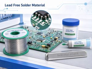
You may also like

PCB and PCBA Manufacturer Israel: Top 5 Companies to Compare

September 8th, 2026

A search for PCB and PCBA manufacturer Israel usually begins with a practical goal: find one company that can turn released board data into working assemblies without forcing your team to manage a PCB factory, component suppliers and an assembly house separately. The right choice can shorten communication, make quotations easier to compare and prevent fabrication or sourcing decisions from disrupting assembly.

Israel offers established local PCB and electronics manufacturers, while overseas production gives eligible projects another combination of technology, capacity and cost. This guide compares five Israel-based companies, explains when local production matters and shows where EBest Circuit can support Israeli customers as a China-based PCB and PCBA manufacturer. EBest is not an Israeli manufacturer, so projects that require domestic production should use a qualified local route.

PCB and PCBA manufacturer Israel
PCB and PCBA manufacturing support for projects serving Israel.

What Can a PCB and PCBA Manufacturer Serving Israel Deliver?

A capable combined supplier should give you one coordinated path from approved manufacturing files to inspected PCBAs—not a bare PCB followed by an unrelated assembly service.

With one coordinated PCB and PCBA supplier, you can:

  • Buy the required finished result: bare PCBs, assembled PCBAs, programmed assemblies or box build.
  • Keep production data aligned: PCB files, BOM and placement data follow the same approved build.
  • Resolve changes earlier: stack-up or sourcing issues can be reviewed before they affect assembly.
  • Retain control over alternatives: substitute materials and components remain subject to customer approval.
  • Match inspection to the assembly: inspection is selected according to the board and solder-joint risks.
  • Start repeat orders from an approved baseline: confirmed materials, components and production requirements remain connected.

Some suppliers manufacture boards, some specialize in PCBA, and others use partner factories. Compare them by the finished result and responsibility they accept—not simply by whether their website mentions both PCB and PCBA.

Top 5 PCB Manufacturers in Israel for PCB and PCBA Projects

These five companies represent different ways to source PCB and electronics manufacturing in Israel. The order is not a quality ranking. The useful question is which operating model best matches your project.

Company Main focus Most relevant for
Nistec / Eltek PCB, PCBA and integration Local support from board to product
PCB Technologies Rigid, flex, rigid-flex and PCBA Advanced boards with assembly
H.A Micro NPI, SMT, testing and rework Local prototype-to-production EMS
HANZA BMK Israel High-reliability EMS Engineering-led manufacturing
Sanmina Israel Electronics and system integration Builds extending beyond PCBA

Published capability is only a starting point. Confirm where your PCB will be fabricated, where it will be assembled and whether any critical operation is subcontracted. Two companies can both advertise PCB and PCBA services while offering very different production routes.

Should Israeli Projects Use Local or Overseas PCB and PCBA Production?

Choose local production when the project must remain in Israel. Consider overseas production when it is permitted and offers a better combination of PCB technology, assembly capacity, cost or supply flexibility.

Your priority Route to review first
Domestic-production requirement Israel-based manufacturing
Controlled technical data Approved local facility
Frequent on-site cooperation Local supplier
Wider PCB technology choice Compare local and overseas options
Integrated sourcing and PCBA Compare complete supplier scope
Lower total production cost Qualified overseas option

Local manufacturing is stronger when a contract specifies production in Israel, technical data cannot leave the country, a particular facility is qualified or frequent in-person support is essential.

Overseas production is attractive when international sourcing is permitted and the project needs wider PCB choices, sourcing and PCBA under one commercial route.

Compare total project impact: engineering response, material and component availability, assembly, inspection, freight and supplier-management time. The lowest bare-board price may not produce the lowest assembled cost.

PCB and PCBA manufacturer Israel
Compare local and overseas production according to the project requirements.

Which Certifications Matter for PCB and PCBA Projects in Israel?

The relevant certifications depend on the product and its market. A general industrial assembly does not require the same quality framework as a medical, automotive or aerospace product.

Project type What customers commonly review
General industrial ISO 9001 and defined IPC criteria
Medical-device supply chain ISO 13485 where required
Automotive IATF 16949 where applicable
Aerospace AS9100 and project approvals
Commercial electronics Quality system and material declarations

ISO 9001, ISO 13485, IATF 16949 and AS9100 relate to quality systems and industry scope. IPC-A-600 and IPC-6012 address bare boards, while IPC-A-610 and J-STD-001 are commonly applied to assembly acceptance and soldering.

The value lies in relevant evidence, not the number of logos. The certificate should cover the facility and work being ordered, while the purchase requirements define workmanship and acceptance criteria.

A manufacturer’s certificate does not certify the finished product. Product approval remains with the product owner and relevant authorized parties.

How Does EBest Circuit Reduce Production Risk for Israeli Projects?

EBest Circuit reviews how PCB fabrication, sourcing and assembly affect one another before production. Customers gain fewer late questions and uncontrolled changes.

Problems are found while they are still easier to solve. A difficult PCB feature, unclear stack-up or footprint conflict is more useful when identified before material release than after assembled boards fail inspection.

Customers retain control over component decisions. If a BOM item is unavailable or carries an unacceptable lead time, EBest can identify the issue and propose an alternative. The customer or authorized design owner decides whether it is acceptable.

Inspection matches the assembly. SPI can evaluate paste deposition, AOI can inspect visible placement and solder conditions, and X-ray can be used for hidden joints beneath packages such as BGA or QFN. The plan follows the board’s risks rather than a generic equipment list.

Repeat orders start from an approved baseline. Material choices, component decisions, files and inspection requirements remain connected to the build.

EBest supports manufacturability review, approved-BOM sourcing, PCB fabrication, assembly and agreed inspection or testing. Product architecture, regulatory decisions, firmware and final product approval remain with the customer.

PCB and PCBA manufacturer Israel
Inspection should match the assembly risks and acceptance requirements.

PCB and PCBA Manufacturing Case Study for an Israeli Customer

An Israeli customer ordered a six-layer FR-4 PCB for AI hardware. Its construction supported dense routing, stable assembly and efficient transfer into PCBA.

Item Requirement
Application AI hardware
Board 6-layer FR-4, 1.6 mm
Copper 1 oz inner / outer
Material Tg 170
Finish ENIG
Appearance Green mask, white legend
Delivery 101 four-up panels
Quantity 404 boards

Why did this construction fit the AI hardware application?

Six layers gave the design more room to separate signal routing, power and ground than a simpler two- or four-layer board. That is useful in compact AI hardware where processors, memory, power circuits and high-speed interfaces compete for routing space. The exact signal and power performance still depends on the released stack-up and layout; layer count alone does not guarantee it.

Tg 170 FR-4 provided greater thermal margin than a lower-Tg standard material during soldering and repeated heating. This was relevant to hardware that may place computing and power components on the same assembly. The 1 oz copper construction provided a practical balance between routing, current carrying and manufacturability, although trace width, copper area and cooling still determine actual current and temperature performance.

ENIG created a flat solderable surface suited to dense SMT and fine-pitch component areas. The familiar 1.6 mm thickness also simplified mechanical integration with standard connectors and mounting hardware specified for that board.

The customer received 100 production panels plus one additional four-up panel, giving 404 boards in total. Four-up delivery reduced individual-board handling and provided a repeatable format for solder-paste printing, placement and inspection. The benefit was an AI hardware PCB delivered in a form that supported the next PCBA step—not simply 404 loose boards.

PCB and PCBA manufacturer Israel
A four-up PCB panel and assembled AI hardware board prepared for production.

Why Choose EBest Circuit for PCB and PCBA Projects in Israel?

EBest Circuit is a practical option for Israeli customers that can use overseas manufacturing and want PCB fabrication, sourcing, PCBA and inspection coordinated through one supplier.

  • Less coordination: one project connects PCB, BOM and assembly questions.
  • Earlier decisions: manufacturability and availability issues appear before production.
  • Controlled substitutions: alternatives remain subject to customer approval.
  • Better technical fit: PCB technology and assembly needs are reviewed together.
  • Easier repeat orders: the approved production basis can move forward with the project.

The reason to request a quotation is not that EBest claims to suit every Israeli project. It is that customers without a domestic-production requirement can compare a China-based integrated route with local options. That comparison may reveal a better fit for technology, sourcing, capacity or total project cost.

Send your Gerber or ODB++ data, fabrication drawing, BOM, placement file, assembly drawing, quantity and test requirements to sales@bestpcbs.com. EBest can review the actual build and respond according to the released scope.
FAQs About PCB and PCBA Manufacturing for Israel

Is EBest Circuit a PCB and PCBA manufacturer in Israel?

No. EBest Circuit is based in China and serves customers in Israel. Projects requiring domestic Israeli production should use a qualified local manufacturer.

Can one company supply both bare PCBs and assembled boards?

Yes. It may provide both directly or coordinate them within one group or supply chain. Confirm the production locations and responsibility for the finished assembly.

Is local PCB production always faster for an Israeli customer?

Not necessarily. Total lead time also depends on engineering review, material availability, component procurement, assembly capacity and testing. Compare the complete schedule, not transit time alone.

When should an Israeli project avoid overseas manufacturing?

Avoid it when contracts, data-control rules, security requirements, customer qualifications or service obligations require production in Israel or another approved facility.

Which certification should a medical PCB or PCBA supplier have?

ISO 13485 may be required when the supplier participates in a medical-device quality system. The exact requirement depends on the approved supply chain and product obligations, and the certificate scope must match the work.

Can EBest Circuit source all PCBA components?

EBest can support BOM sourcing subject to availability and the agreed purchasing model. The customer should approve alternatives when a specified manufacturer part number cannot be supplied.

Which inspections are useful for PCB assembly?

SPI is useful for solder paste, AOI for visible placement and solder conditions, and X-ray for hidden joints. The best combination depends on the packages, board design and acceptance requirements.

What should you compare between PCB and PCBA quotations?

Compare the finished deliverable: PCB construction, material, sourcing, assembly, inspection, testing assistance, records, lead time, shipping terms and exclusions. Unit price alone does not show whether two quotations cover the same work.

If your search for PCB and PCBA manufacturer Israel is intended to find both local companies and an overseas alternative, compare every candidate against the same project outcome. For an EBest Circuit review, send the released manufacturing package to sales@bestpcbs.com.
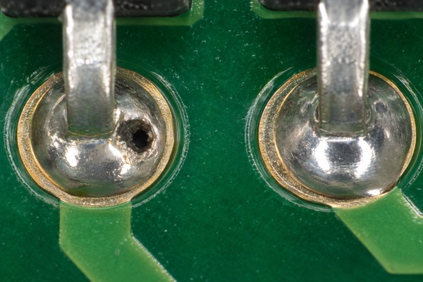
You may also like

GPU Shortage: RTX 5090 Sourcing Risks for Box Build

September 7th, 2026

The September 7, 2026 GPU shortage snapshot matters to EBest Circuit (Best Technology) when a customer-approved graphics card is part of a Box Build order. RTX 5090 sourcing does not change how we manufacture the surrounding PCBs, but uncertain availability can delay material release, force another mechanical and electrical review, and change the agreed system test. We therefore treat the GPU as a separately approved high-value item within the complete assembly, not as a component that can be substituted by chipset name alone.

GPU shortage and RTX 5090 sourcing for a professional Box Build project

What Does the September 7 RTX 5090 Price Snapshot Show?

The observed listings showed a clear difference between Founders Edition reference prices and orderable add-in-board models. This is a dated channel snapshot rather than a market average. Each row preserves the region, seller, exact item, price and availability observed on September 7, 2026.

Region Channel and exact item Observed price and status Comparison basis
United States NVIDIA Marketplace, GeForce RTX 5090 Founders Edition, MPN NVGFT590 $1,999.00; out of stock Matched NVIDIA’s US launch starting price but was not orderable.
United States Best Buy, Founders Edition, model 900-1G144-2530-000, SKU 6614151 $1,999.99; sold out $0.99 above the US launch reference but was not orderable.
United States Newegg, MSI RTX 5090 32G GAMING TRIO OC, item 14-137-919 $4,699.99; listed in stock An AIB model, so it is not a like-for-like comparison with the Founders Edition.
United Kingdom Scan, MSI RTX 5090 32G GAMING TRIO OC, scan code LN155275 GBP 4,679.99; listed in stock The same MSI model as the US sample, but currency, tax and regional terms differ.

The figures do not support one universal claim about the RTX 5090 market price. Founders Edition and factory-overclocked AIB cards differ in cooler design, dimensions, power settings and commercial terms. For a Box Build order, the useful conclusion is narrower: the project cannot assume that its approved model will be available at the original budget and delivery date.

Illustration comparing availability for the same high-end GPU across two regional channels

Why Does GPU Availability Matter to a Box Build Manufacturer?

A discrete high-end GPU enters the Box Build during system integration, but its availability affects decisions made before assembly starts. We need the approved manufacturer part number and the selected material-supply model before confirming the integration schedule.

  • Material release: The assembly schedule must reflect when the approved GPU will actually arrive and pass the agreed receiving checks.
  • Mechanical fit: Card length, height, slot width and power-connector position affect the enclosure, brackets and cable clearance.
  • Power and thermal inputs: The selected card affects the PSU, connector arrangement, airflow plan and system-level thermal check.
  • Test preparation: The operating system, driver, display outputs and acceptance load must match the approved configuration.
  • Change control: A different RTX 5090 model is an engineering change when it alters any of these inputs, even if the GPU family name is unchanged.

This is the direct connection between the news and our manufacturing work. The channel price itself is outside our control; the material handoff, integration inputs and agreed production tests are the parts that must be controlled within the Box Build project.

What Must Be Revalidated When the Approved GPU Changes?

Substituting one board partner’s RTX 5090 for another can affect more than the purchase price. Before we release a revised configuration, the customer and our engineering team should confirm the items that changed.

Review area Required input Manufacturing consequence
Enclosure fit Card dimensions, slot width, bracket and connector location Confirms clearance, retention and cable routing.
Electrical interface Power connector, PSU rating and motherboard compatibility Confirms the released cable and power configuration.
Thermal design Cooling layout, airflow direction and operating load Determines whether the enclosure and fan plan need another review.
Software setup Approved driver, firmware and operating-system image Keeps the functional-test configuration consistent.
Acceptance test Boot, output, load and temperature criteria agreed for the system Defines what our production test can verify after integration.

These checks do not require BestPCBs to forecast GPU prices or recommend a retail channel. They ensure that a customer-approved change does not create a preventable assembly or test problem.

How Should GPU Availability Be Reflected in the Production Schedule?

The GPU delivery date should not automatically hold every part of the project, but the manufacturing plan must separate work that has stable inputs from work that depends on the final card. This prevents an uncertain delivery promise from becoming an unexamined Box Build completion date.

  • PCB and PCBA production: These stages can proceed when the electrical interfaces, board revisions and approved BOM are frozen independently of the GPU model.
  • Enclosure and cable preparation: Production can proceed only after the selected card’s dimensions, bracket and power-connector position are confirmed.
  • Final integration: The schedule should begin from the confirmed receipt of the approved GPU and completion of the agreed incoming checks.
  • System testing: Test time should follow installation and use the approved driver, operating-system image and acceptance criteria.

When these dependencies are visible, we can plan the surrounding manufacturing work without claiming that an unreceived GPU is available. If the approved model changes, only the affected steps need to be reviewed and rescheduled.

Who Should Supply the GPU for a Box Build Project?

Box Build procurement can use full-turnkey, partial-turnkey or consignment arrangements. For a volatile and high-value item, the appropriate model depends on who has the approved source, who accepts the quoted price and who owns the supplier warranty.

Supply model Customer decision Our manufacturing role
Customer supplied material Purchase the approved GPU and retain the original supplier and warranty relationship. Receive, record, store, kit, install and test it according to the agreed project requirements.
Customer-nominated source Approve the exact seller, part number, price and commercial terms before purchase. Purchase only after approval, then process the item through the agreed receiving and assembly flow.
Assembler sourcing Approve the quoted item, validity period and any permitted alternative. Source against the approved BOM when availability and terms can be confirmed for that order.

EBest Circuit (Best Technology) does not claim to manufacture GPUs or hold RTX 5090 inventory. Availability and warranty must be confirmed for the exact seller and order date. Our responsibility is limited to the sourcing scope accepted in the order and the manufacturing work performed on the complete assembly.

Customer supplied material control from receipt through Box Build testing

What Information Should Accompany a Customer-Supplied GPU?

Customer supplied material needs a clear manufacturing handoff. For component traceability within the Box Build record, the customer should identify the approved manufacturer part number, quantity and any serial-number mapping required for its service process.

Incoming inspection and component traceability for a high-value GPU
  • Approved manufacturer part number and permitted revision or alternative.
  • Expected quantity and any project-specific serial-number requirement.
  • Packaging condition or handling requirement that must be checked at receipt.
  • Instructions for discrepancies, transit damage or a unit that fails the agreed incoming or system test.
  • The party responsible for supplier contact, return authorization and replacement material.

Our receiving record can document what entered the manufacturing flow and which unit was installed when serial mapping is required. It does not certify the internal authenticity of a GPU or replace the original supplier’s warranty.

What Can EBest Circuit Support Around the GPU?

At EBest Circuit (Best Technology), our relevant work is the electronics and assembly around the approved GPU. Our PCB assembly service supports SMT, through-hole and mixed assembly for control, power and interface boards. We can manufacture the project’s FR4 control and I/O PCBs, and high-Tg PCB construction is available when the board design and operating conditions justify it.

Depending on the approved project scope, we can also support component sourcing, incoming material checks, cable and enclosure integration, final assembly and agreed functional testing. SPI, AOI and X-ray apply where appropriate to the PCBA being manufactured; they should not be presented as proof of GPU authenticity. The exact Box Build test must be defined from the customer’s system requirements.

What Should Be Confirmed Before Production Release?

Before production release, the project should identify the exact GPU, supply model, expected delivery date, permitted alternatives, enclosure and power inputs, required serial records, warranty contact and system acceptance test. Once those items are agreed, we can plan the surrounding PCB, PCBA and Box Build work without treating an uncertain retail listing as confirmed production material.

For a project affected by the current GPU shortage, send the approved system BOM and assembly requirements to sales@bestpcbs.com. We will review the manufacturing scope and identify which GPU-related inputs must be supplied or approved before the order is released.
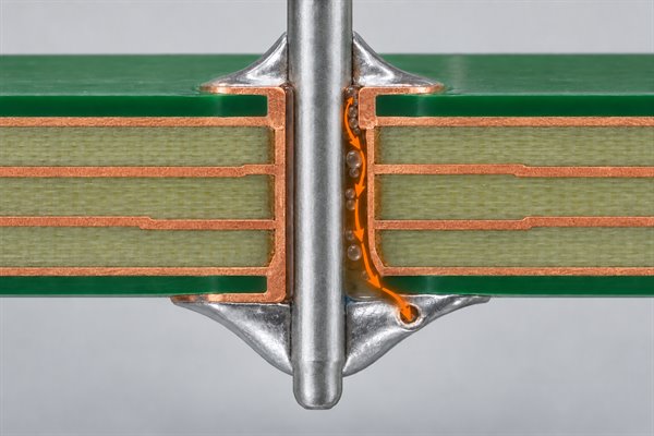
You may also like

Vapor Phase Soldering: Process, Profiles & Practical Limits

September 4th, 2026

Vapor phase soldering heats a PCB assembly by condensing hot vapor on its cooler surfaces. The released heat melts the solder alloy in the paste and forms the joints. Also known as condensation soldering or vapor phase reflow, this method can help when large, slow-heating parts share a board with small, temperature-sensitive components.

Its main appeal is controlled heat transfer across that mixed assembly. The fluid limits the heating temperature; it does not guarantee a good solder joint. Fluid selection, the measured board profile and inspection results still determine whether the process suits the PCB.

Vapor phase soldering, illustrative laboratory reflow equipment and a populated PCB carrier with the article title

How Does Vapor Phase Soldering Work?

When vapor condenses on the PCB, it releases latent heat directly to the board and components. The vapor comes from a purpose-made heat-transfer fluid, not water. That fluid carries heat; the solder paste supplies the metal that joins each component termination to its pad.

In a conventional saturated-vapor machine, heaters boil the fluid beneath a controlled vapor zone. A carrier holds the assembly in that zone while condensate forms on its surfaces and drains back into the reservoir. Some machines instead meter fluid into a process chamber, so the loading and vapor-delivery sequence depends on the equipment.

Condensation heating falls as the board approaches the vapor temperature. At a given pressure, the fluid’s boiling point sets the temperature ceiling for this heating method. A component rated below that temperature can still be damaged, while a heavy copper area may take longer to reach soldering temperature.

Vapor phase soldering, conceptual chamber cutaway with a populated PCB on a carrier above heat-transfer fluid and condensate returning to the reservoir

What Are the Steps in Vapor Phase Soldering?

After solder paste printing and component placement, the board moves through loading, preheating, reflow and cooling. Vacuum may be added during the molten-solder stage when the process calls for it.

  • Prepare the board before heating. Verify the board revision, paste, component orientation and moisture-handling requirements. Inspect the deposits and placement: reflow cannot repair missing paste or a wrongly fitted part.
  • Load the board on a stable carrier. Allow for its outline, weight and underside components. Supports must hold the assembly through heating and cooling without pressing on parts.
  • Preheat at the required rate. Adjust preheat or vapor delivery to suit the paste and component limits. The measured ramp and soak should allow flux activation and volatile release without excessive thermal stress.
  • Bring the critical joints through reflow. Hold them within the required temperature and time limits. Check both the slowest-heating joints and the most heat-sensitive components.
  • Apply vacuum only when the process includes it. Coordinate pressure and timing with the molten-solder interval. Save the pressure cycle alongside the temperature trace so the result can be repeated.
  • Cool before unloading and inspection. Recover the working fluid and keep the board supported as the joints solidify. Inspect accessible and hidden joints using the specified methods, then complete the electrical tests.

Vapor phase reflow does not require vacuum. A non-vacuum machine can produce acceptable joints when the profile, materials and assembly meet the product’s requirements.

What Fluid Is Used in Vapor Phase Soldering?

Common vapor phase soldering fluids are perfluoropolyethers, or PFPEs. The selected grade sets the nominal vapor temperature at the operating pressure. Grades with similar names or boiling points are not necessarily interchangeable.

Galden LS/HS grades, for example, are designed for vapor phase soldering; general-purpose HT grades have different distillation-range and vapor-temperature controls. Choose a soldering fluid that matches the machine specification, solder paste and component limits.

A 230°C fluid will not become a 245°C heat source because the board stays in longer. In saturated vapor at the specified pressure, extra dwell gives colder joints more time to approach the vapor temperature. If the paste needs a peak the fluid cannot provide, change the fluid, paste or process.

Include fluid recovery, maintenance and consumption in the operating-cost estimate. Follow the current technical and safety data for machine compatibility, hot-fluid handling and disposal; chemical inertness does not remove those precautions.

How Do You Measure a Vapor Phase Soldering Profile?

Measure temperatures on the assembly, rather than judging the profile from the vapor reading alone. A vapor phase soldering temperature profile needs to show how the critical joints and components heat, dwell and cool.

Place thermocouples at a large thermal pad or copper-rich area, a small fast-heating location and a temperature-sensitive component. Identify whether each sensor measures a joint or a package body—their limits may differ. Use the intended carrier and a representative production load.

Vapor phase soldering, illustrative PCB with thermocouple leads connected to a logger with a blank display
  • Heating rate and soak: look for uneven heating. If small parts heat much faster than a large pad, adjust preheat or vapor delivery and measure again. Keep the ramp and dwell within the paste and component limits.
  • Peak temperature: both hot and cold locations must pass. The coldest critical joint must reach the paste’s process window while the hottest monitored component stays within its limit.
  • Time above liquidus: measure each critical joint. Too little time above the alloy’s liquidus temperature can leave incomplete wetting. Extending that interval also affects flux behavior and intermetallic growth, so use the paste’s specified window.
  • Cooling: keep recording until the joints solidify. Check the specified cooling limits and keep the assembly supported. Stopping the trace at peak temperature leaves this part of the profile unverified.

There is no universal temperature recipe for VPS. Indium Corporation gives a preferred peak of 230–240°C for the SAC pastes in its vapor-phase application note, and 30–90 seconds above liquidus for the Pb-free no-clean pastes it describes. Those ranges apply to the materials discussed. Set your trial from the current paste data sheet and the most restrictive component limits.

What Causes Common Vapor Phase Soldering Defects?

Trace defects through paste printing, placement and the measured profile before changing the heat settings. Note which parts fail and when the problem first appeared. A lifted resistor and a solder bridge may need very different corrections.

  • Tombstoning: compare the two ends of the lifted part. Unequal wetting forces can pull a small resistor or capacitor upright. Check paste volume, placement and whether the copper connections make one pad heat sooner. If printing and placement are balanced, try a gentler ramp within the paste’s limits and recount defects at those locations.
  • Component shift: find out when the part moves. Check its position and paste alignment before reflow. Movement that begins only with vacuum calls for a pressure-trace review. Trial a less abrupt evacuation cycle without losing the required soldering conditions, then inspect for beads and bridges as well as alignment.
  • Excessive voiding: check the joint before increasing vacuum. Poor wetting or insufficient solder can leave unfilled areas as well as trapped gas. Compare X-ray patterns, deposit volume, paste condition and the joint profile. Once those are stable, assess a controlled vacuum trial using the same imaging method and acceptance limit.
  • Solder balls or spatter: review paste handling and the heating ramp. Rapid heating can contribute to volatile release and spatter; poor coalescence can leave separate particles. Check deposit shape and trial the recommended preheat conditions. If the defect begins with vacuum, review the evacuation rate too.
  • Incomplete wetting: separate a heat problem from a surface problem. Verify joint peak temperature and time above liquidus. If both meet the material requirements, investigate pad and termination solderability, contamination, paste condition and flux performance before adding heat.
  • Bridging: correct excess paste or placement offset first. Look for paste between adjacent pads and misaligned parts. If both printing and placement are sound, investigate slump or movement during heating and vacuum. Change one suspected cause at a time so the next build shows whether it helped.

Compare defect counts across similar batches, not just one clean board. Keep an unchanged reference build where practical and inspect the same locations after each adjustment. Repeat at representative production loads before treating the correction as stable.

How Does Vacuum Vapor Phase Soldering Reduce Voids?

Vacuum lowers the pressure around molten solder, helping trapped gas expand and escape before the joint solidifies. Paste control, pad design and wetting remain important because vacuum cannot correct every cause of an unfilled joint.

The pressure level, evacuation rate, dwell and solder temperature work together. An abrupt pressure change can disturb the solder or shift components. More aggressive vacuum is not automatically a better process.

Where practical, compare the existing process with VPS both with and without vacuum. Keep the board, paste, stencil and inspection method unchanged. Measure void area and location, then inspect for displaced parts, beads, bridges and insufficient solder.

Accept a low-void result only against a defined measurement method and limit. Agree which joint area is measured and how the percentage is calculated. Use suitable X-ray inspection of hidden solder joints to assess the trial boards; neither a machine’s advertised figure nor an X-ray result alone establishes lifetime reliability.

Vapor Phase vs Convection Reflow: What Is the Difference?

Vapor phase uses condensation to deliver heat; convection reflow uses circulating hot gas. Both reflow solder, so VPS is a type of reflow soldering rather than an alternative to reflow itself.

Process factor Vapor phase Convection reflow
Heat delivery Vapor condenses on cooler surfaces and releases latent heat. Circulating heated air or nitrogen transfers heat to the assembly.
Profile control Fluid grade, preheat, vapor delivery, exposure and pressure depend on the machine. Zone temperatures, gas flow and transport speed shape the profile.
Mixed thermal mass Strong condensation heat transfer can help heat large and small features within one process window. Zone and transport settings must bring cold joints into range without exceeding hot-part limits.
Process atmosphere The working-fluid vapor provides an inert environment in the soldering zone. Air and nitrogen configurations are available.
Void reduction A vacuum option can remove gas while solder is molten. Selected systems also include vacuum; it is not exclusive to vapor phase.

Compare joint quality, temperature spread and accepted boards per hour on the same assembly. Keep the board revision, paste, placement quality and inspection criteria consistent. Batch and inline handling are separate choices; commercial VPS equipment is available in both forms.

When Should You Use Vapor Phase Soldering?

Consider VPS when getting a cold joint hot enough pushes another component too close to its temperature limit. That conflict in the measured profile gives a clearer reason to try the process than board size, package name or order volume alone.

  • Large boards with uneven heating. Power planes, thick copper and large connectors heat differently from small chip components. A useful VPS trial should show a smaller temperature spread at the critical locations while all monitored parts stay within their limits.
  • BGA packages with difficult thermal profiles. Vapor phase soldering for BGA assemblies can help heat a large package and its underlying joints. Pad design, paste deposits, warpage and moisture still affect the result, so combine board profiling with hidden-joint inspection.
  • Power devices where voids affect the thermal path. A vacuum-capable process may help large soldered thermal pads. Define the X-ray method and joint-specific limit before the trial; void location and the largest void can matter alongside total void area.

Keep convection if it already delivers acceptable joints, a repeatable profile and the required output at a suitable cost. Rule out printing, placement and material problems before changing the heating method. If voiding is the only remaining issue, compare vacuum options in both types of equipment.

A difficult low-volume board may justify VPS for thermal control alone. In repeat production, weigh any quality improvement against loading, cooling, inspection and fluid costs. The trial needs to show an improvement worth the added cost or cycle time.

What Are the Disadvantages of Vapor Phase Soldering?

The main drawbacks are fluid costs, equipment costs, setup work and cycle time that varies with the load. Efficient heat transfer is useful only when its rate stays within the assembly’s limits.

  • The board can heat too quickly. Even a fluid with the right boiling point needs controlled preheating and exposure. Test the ramp and dwell at the intended load, where fast-heating parts may approach their limits sooner.
  • The fluid temperature may not suit every material. It may be too low for the paste or too high for a component. Resolve conflicting limits before production; a longer dwell cannot fix that mismatch.
  • Fluid recovery adds running costs. The initial charge, carry-out losses, filtration and maintenance all count. Compare consumption for the proposed load and handling method as well as the fluid purchase price.
  • Cooling and handling can limit output. Include loading, preheat, vacuum, cooling and unloading in the cycle estimate. A short reflow step alone does not tell you how many boards the machine can deliver.

Normal moisture-control requirements still apply. Staying below the fluid’s boiling point does not prevent damage from trapped moisture, excessive exposure or an unsuitable material.

How Do You Verify Vapor Phase Soldering Quality?

A good temperature trace must be backed by acceptable joints and the required test results. Set the acceptance limits before the trial, then keep the following information together so the approved build can be repeated.

  • Start with a defined board and material set. Keep the PCB and assembly revisions, construction, component list, paste product and lot, solder alloy and fluid grade together with their temperature, moisture and joint-acceptance limits. Resolve any conflict before running the trial.
  • Make the loading arrangement repeatable. Note the machine, carrier, supports, board orientation and batch size. Mark sensor positions on a drawing or photograph, including whether each measures a joint or package body. Later profiles can then be compared on the same basis.
  • Save the measured curves and their recipe. For each critical location, retain the ramp, peak, time above liquidus and cooling trace against its limits. A vacuum build also needs pressure, evacuation rate, dwell and timing relative to the molten-solder interval.
  • Keep inspection results tied to the boards inspected. Record the sample count and reference designators, visual or automated optical inspection findings, and required X-ray views. Void results need the measured area, calculation method and limit. Include bridges and shifted parts, even if voiding improves.
  • Test the assemblies and repeat the build. Retain the test procedure, limits and results for each board or batch. Repeat at representative loads using a sample plan matched to product risk. Functional testing alone does not qualify every joint; reliability or destructive tests may also be needed.
  • Define what requires another trial. Name the approver and any unresolved deviations. Changes to paste, fluid, major components, copper construction, loading or recipe may require a new profile or qualification review. Keep the approved settings and supporting results accessible to production.

A trial fails if fixing the cold joint overheats another component. Adjust the available controls, measure both locations again and repeat the affected inspection and tests. The accepted process must suit the whole assembly.

How Do You Choose a Vapor Phase Soldering Machine?

Choose a machine that fits the populated board, can achieve its profile and meets the required output. Compare price only after the quotations include the same necessary functions.

A compact batch vapor phase reflow oven may suit laboratory work or short runs, while an inline system may fit a continuous line. In either case, use the actual board and loading arrangement to judge handling, process control and cycle time.

  • Usable board space and support. Supply panel dimensions, assembly weight, component heights on both sides and support restrictions. The usable carrier area and clearances matter more than the chamber’s outside dimensions.
  • Temperature and vacuum controls. Compare supported fluid grades, heating adjustments, measurement features and pressure-cycle control. For a narrow process window, ask for a trial on a representative board.
  • Fit with the production line. Check loading, cooling, line interfaces, recipe access and process records. Estimate output from the full cycle and planned utilization.
  • Installed and operating costs. Include required options, fluid charge and losses, filtration, utilities, maintenance, labor, qualification and inspection. This makes the machine-price comparison meaningful.

When outsourcing PCB assembly, confirm access to VPS equipment before specifying the process in an order. Ask where the work will be done and which qualification records are included; general SMT capability does not establish VPS availability.

FAQ About Vapor Phase Soldering

Q1: Are vapor phase soldering and vapour phase soldering different?

A1: They are spelling variants. “Vapor” is American English and “vapour” is British English. VPS, vapor phase reflow and condensation soldering commonly refer to the same heating principle. Individual machines may use different vapor-delivery and profile-control methods.

Q2: Does the process need nitrogen?

A2: The basic condensation process does not need a separate nitrogen supply. The working vapor can provide the inert soldering atmosphere. Some machines still use nitrogen for chamber or cooling functions, so confirm the utilities for the model and configuration being considered.

Q3: Can double-sided PCBs use vapor phase reflow?

A3: Yes, with a suitable assembly sequence and carrier. Allow clearance for underside components and consider how they will stay in place during the second heating cycle. Heavy parts may need another sequence or retention method. Trial the populated board on its intended carrier and account for cumulative thermal exposure.

Q4: Does the working fluid remove the need to clean flux residue?

A4: No. Recovering the working fluid does not remove the need to assess flux residue. Cleaning depends on paste chemistry, residue behavior and later operations such as conformal coating. Check the assembled product against its cleanliness and material-compatibility requirements.

Q5: Can vapor phase equipment be used for rework?

A5: Some systems support desoldering and repair with suitable tools and a qualified process. Other components and underside joints also experience the additional thermal cycle. Check their limits and moisture history, then inspect and retest the repaired circuit. Identify the fault before deciding to reflow the board.

Conclusion

Choose vapor phase soldering when trials show a useful improvement in thermal control or joint quality at an acceptable production cost. Match the fluid to the paste and component limits, measure the board profile and evaluate vacuum if voiding remains a problem. A working convection process may already be the better fit.

For a free DFM review with BestPCBS, send your Gerber or ODB++ files, BOM with exact part numbers and allowed alternatives, assembly drawing, quantity, target delivery and inspection requirements to sales@bestpcbs.com.
Include the solder alloy, temperature-sensitive parts and any voiding limit. If VPS is required, ask the team to confirm the process and availability for your project before quotation.

You may also like

When to Use Manual vs Automated PCB Assembly?

September 4th, 2026

Use manual assembly for a few accessible parts, frequent prototype changes or work that needs individual handling. Choose automated PCB assembly for dense layouts, precise component placement and repeat production. Quantity alone is a poor guide: a few fine-pitch boards may need machine placement, while a large production run may still include hand-fitted connectors or cables. Start with the parts on the board, then compare setup costs, inspection needs and the cost of each acceptable finished assembly.

Automated PCB assembly, illustrative PCB fixture and tweezers in front of an enclosed placement machine with the article title

What Is Automated PCB Assembly?

Automated PCB assembly uses programmed equipment to apply solder paste, place components and inspect the assembly. In a typical surface-mount technology (SMT) process, parts are placed onto paste deposits and soldered in a reflow oven. Assembly starts with an already fabricated PCB; manufacturing the bare board is a separate process.

Manual assembly can mean hand placement followed by reflow, hand insertion of through-hole parts, or soldering individual joints with a controlled tool. When comparing quotes, ask which of these operations the supplier means by “manual” and how the finished joints will be checked.

How Does the Automated PCB Assembly Process Work?

An automated SMT line prints solder paste, checks the deposits, places components and reflows the solder before final inspection and testing. The files and materials must be checked first: an incorrect part number or feeder assignment can affect every board in the batch.

Automated PCB assembly, component placement machine with tape feeders photographed on the BestPCBS website
  1. Check the files and component kit. Match the bill of materials (BOM), placement file and assembly drawing to the same revision. Confirm part numbers, orientation, approved substitutions and do-not-populate positions. Resolve any difference between the received parts and the BOM before loading the machine.
  2. Print or dispense solder paste. A stencil printer or dispensing system applies paste to the specified pads. Check the stencil or dispensing program against the board revision and package requirements. The deposits need to match the required locations and amounts before parts are placed.
  3. Inspect the paste deposits. Solder paste inspection (SPI) measures features such as deposit height, area or volume, depending on the system. Review deposits outside the set limits and correct the printing problem before placement. SPI checks paste at this stage; solder-joint inspection follows reflow.
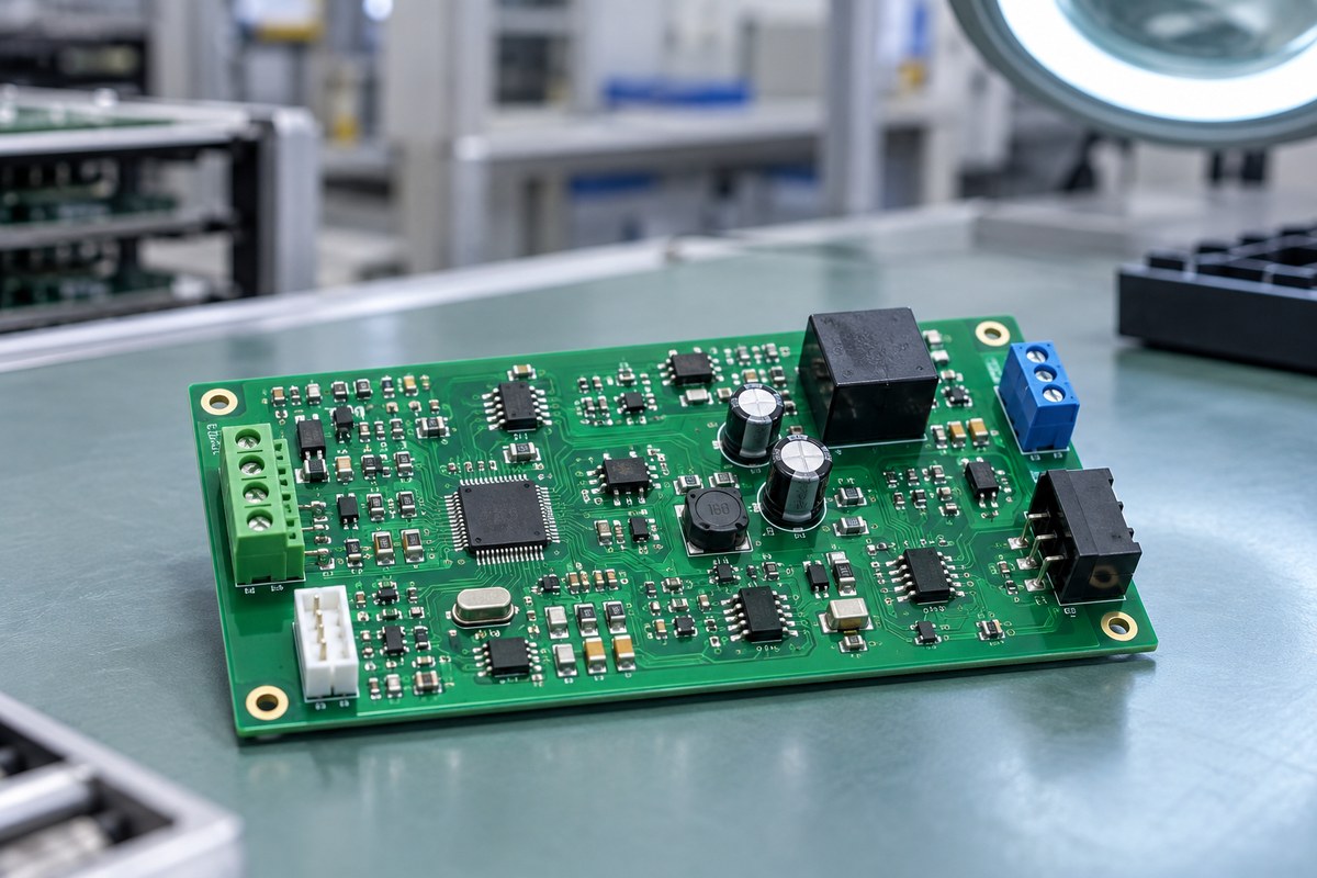
  4. Place the components. The pick-and-place machine takes parts from feeders and uses vision and board reference marks, called fiducials, to position them. Verify feeder assignments and component orientation on the first board. Correct misplaced, missing or wrong parts before continuing the batch.
  5. Reflow the solder. The oven heats and cools the assembly to form the solder joints. Measure the board’s thermal profile and check it against the solder-paste requirements and component temperature limits. Keep the measured profile with the build records instead of assuming another board’s oven settings will work.
  6. Finish and test the assembly. Inspect the reflowed board and complete any remaining through-hole soldering or mechanical fitting in the agreed order. Repeat affected inspections after work that could disturb earlier joints. Record the required electrical and functional test results before releasing the finished boards.

An automated PCB assembly line commonly includes a paste printer, SPI system, pick-and-place machine, reflow oven and optical inspection station. The quoted service may stop short of a finished, tested product. Confirm whether X-ray inspection, firmware programming, functional testing and enclosure assembly are included where needed.

When Should You Choose Manual PCB Assembly?

Manual assembly often suits early design changes, a few easy-to-handle parts and local repair work. It saves machine preparation only if a technician can reach, solder and inspect the parts reliably.

  • The circuit is still changing. A prototype may need different resistor values, added wires or repeated component replacement. Accessible parts can be changed without setting up a new placement program. Record each approved modification so the next revision reproduces the working circuit.
  • There are only a few accessible parts. Hand placement may take less time than preparing feeders and a machine program for a simple board. Compare the actual placement and inspection labor with the setup charge. A small batch with difficult packages may still favor automation.
  • A few parts need individual handling. Loose wires, unusual connectors or mechanically secured parts may be easier to fit at a manual station. Check soldering-tool access, board support and component temperature limits. For repeat orders, ask whether dedicated feeding or fitting tools would reduce the handwork.
  • A board needs local repair. A technician can investigate a specific fault, replace the affected component and retest that circuit. Define the repair method and checks before starting, and record what was changed. Repeated repairs at the same location also call for a review of the original assembly process.

Manual work still needs electrostatic discharge (ESD) protection, part-number checks, controlled soldering and inspection. If joints sit beneath the package, confirm how solder will be applied and how those hidden joints will be assessed before choosing hand placement.

When Does Automated PCB Assembly Make More Sense?

Automation makes more sense when a board has dense placement, difficult packages or enough repeat work to reuse the setup. Small batches can qualify too: package size and access may matter more than the number of boards.

  • Small components or dense layouts make hand placement difficult. Tight spacing leaves less room for tools and increases placement demands. For quad flat no-lead (QFN) packages, check the PCB lands, paste volume and reflow profile together. Accurate machine placement cannot correct an unsuitable paste deposit.
  • The same design will be built again. Placement programs and inspection settings can be reused after checking for revision changes. Give the assembler the first-order quantity and likely repeat quantities, then ask which setup charges recur. Keep forecasts separate from committed orders.
  • Hand placement is slowing the batch. Measure placement time alongside inspection and testing time. Automation helps throughput when placement is the limiting operation. If functional testing takes longer or components are missing, a faster placement machine will not remove that delay.
  • The work must repeat across shifts. Verified machine settings reduce dependence on each operator’s placement technique. Check the first assembly before releasing the batch: a wrong feeder assignment or program can repeat the same defect on every board.

For high-mix, low-volume production, ask how long component preparation, program verification and line changeover take for each design. These tasks can outweigh the placement time on a short run. For larger runs, check that feeder replenishment, secondary soldering and testing can keep pace with the placement machine.

How Do Manual and Automated PCB Assembly Compare?

Compare both routes for the same board revision, quantity and inspection requirements. Otherwise, a lower unit price may simply cover less work.

Build factor Manual route Automated route
Design changes Accessible changes can be made with limited setup; document every modification. Changed data and programs need verification; stable revisions make reuse easier.
Placement workload Useful for a few accessible parts; labor grows with placements and handling difficulty. Useful for dense or repeated placement; feasibility depends on packages, feeders and tooling.
Special operations Flexible for cables, special fitting and controlled local rework. May require dedicated tooling; suitable repeat operations can justify it.
Cost structure Often less programming effort, with more direct labor per assembly. Setup and tooling are spread across the batch; changeovers still consume resources.
Quality control Needs documented workmanship, inspection and the agreed electrical tests. Needs validated inputs, process monitoring and the same agreed acceptance criteria.

When Is a Hybrid PCB Assembly Process the Best Fit?

A hybrid process suits boards whose SMT components can run through the line together, while a few parts need separate fitting or soldering. The assembler assigns a method to each operation, so the same board can use both automated and manual work.

Consider a hypothetical industrial controller with surface-mount resistors and ICs, a through-hole terminal block and a wired connection to an enclosure. The SMT components can be printed, placed and reflowed together. The terminal block can then use a qualified through-hole soldering operation, while wire attachment and mechanical fitting may remain manual.

Automated PCB assembly, populated PCB with surface-mount ICs, capacitors and several board connectors, photographed on the BestPCBS website

Mixed-technology PCB assembly means the board uses both SMT and through-hole components. It does not necessarily mean manual plus automated work; through-hole insertion and soldering can also be automated.

Ask for the operation sequence before approving a hybrid build. It should show when special parts are fitted, which parts can pass through reflow or cleaning, and when inspection takes place. Later fitting, soldering or board separation may affect joints that passed an earlier check.

When Does Automated PCB Assembly Become Cost-Effective?

Automation becomes cheaper when the savings per board cover its extra setup and tooling costs. Both methods must first meet the board’s assembly and test requirements. There is no universal break-even quantity; use the charges quoted for your order, rather than a machine supplier’s production-speed claim.

A simple batch model is:

Total assembly cost = setup cost + quantity × variable assembly cost per board

The variable cost should cover the same placement, soldering, inspection and test scope. Keep bare boards and components separate if their costs are identical. If a route changes material losses, scrap or rework, include those differences before making a decision.

To compare cost per board, divide each route’s total batch cost by the number of acceptable assemblies delivered. Include setup, secondary soldering and testing before comparing the result with a quoted placement charge.

Illustrative calculation, not a supplier quote: assume the manual route costs $120 to set up plus $18 per board, while the automated route costs $600 to set up plus $6 per board. Both are assumed feasible, with equal test coverage and no difference in material losses.

Break-even quantity = ($600 − $120) ÷ ($18 − $6) = 40 boards

  • At 20 boards: manual assembly totals $480 and automation totals $720. Manual assembly is $240 lower under these assumptions.
  • At 40 boards: each route totals $840. This is the equality point for this example, not an industry threshold.
  • At 100 boards: manual assembly totals $1,920 and automation totals $1,200. Automation is $720 lower, provided the assumptions remain valid.

This example assumes automation has both the higher setup cost and the lower variable cost. With those setup charges, equal or higher automated per-board costs would give no positive break-even quantity. Recalculate if repeat-order setup charges, programming changes, scrap or rework alter either quote.

Check lead time separately from cost. The delivery estimate should include material availability, engineering preparation, the production slot and testing time—not just time on the placement machine.

How Is Quality Controlled in Automated PCB Assembly?

Quality control starts with the correct parts and settings, then checks paste deposits, placement, solder joints and required electrical functions. When the same defect recurs, investigate its cause. Replacing a faulty joint on each board will not correct unstable printing or a wrong machine setting.

Automated PCB assembly, enclosed SINIC-TEK optical inspection station and monitor photographed on the BestPCBS website
  • Check paste before placing parts. SPI flags deposits that are too small, too large or misplaced relative to the programmed limits. Look for repeated failures at the same pads or board locations, then correct the printing setup before more boards enter placement.
  • Inspect visible parts and joints. Automated optical inspection (AOI) checks programmed features such as component position, polarity and visible joints. Review flagged conditions against the acceptance criteria and recheck the program after a design or component change. Electrical testing is still needed to verify the specified circuit behavior.
  • Assess joints hidden beneath packages. Optical inspection cannot directly see joints under ball grid array (BGA) packages. Agree whether the board needs X-ray inspection, what features will be assessed and whether every board or a sample will be checked. An image of a joint does not establish the product’s long-term reliability.
  • Measure the required electrical characteristics. In-circuit testing (ICT) or flying-probe testing can check specified nets, components or measurements where test access allows. Ask which checks the quoted test covers and what limits apply. Compare fixture costs and test time when choosing between methods.
  • Test the required operating functions. Provide the firmware, power conditions, loads, interfaces and pass/fail limits for functional testing. Specify which results must be recorded for each unit. A test at one operating point covers that condition, not every function or environmental limit.
  • Keep the build and repair records. Record the board revision, agreed lot or serial identifiers, repairs and subsequent checks. Specify any additional traceability requirements before ordering so the assembler can include the records, handling and time in the quote.

Select inspection and testing for the board’s packages, functions and failure risks. List each required check, when it occurs and what constitutes a pass. If two suppliers quote different test coverage, resolve that difference before comparing unit prices.

What Should You Ask an Automated PCB Assembly Manufacturer?

Ask how the supplier will assemble your board, approve the first unit and control later batches. The answers should refer to your files and parts, rather than repeat a general equipment list.

  1. Identify parts that need special work. Ask which parts need manual fitting, separate soldering or dedicated tooling, and why. Resolve concerns about package handling, temperature limits or tool access before the batch starts.
  2. Agree how the first assembly will be approved. Specify the part-number, polarity, workmanship and test checks required before the remaining batch proceeds. Name who can resolve a discrepancy and where the approval will be recorded.
  3. Check revision control for repeat orders. Ask how BOM changes and approved substitutes reach the placement and test programs. Put the released revision on each repeat order so an old sample or program cannot silently become the build instruction.
  4. Confirm what the price includes. Separate setup, tooling, assembly, testing and materials where applicable. Ask who owns the tooling, which setup costs recur and how many extra customer-supplied parts are needed for setup or handling losses. These details can change the cost of both the first batch and repeat orders.

What Files Do You Need for an Accurate PCBA Quote?

Send matching PCB files, placement data and a BOM, along with quantities, delivery dates and test requirements. Missing or conflicting revisions can leave the assembler pricing a different board from the one you intend to order.

  • PCB files and component positions. Send Gerber and drill files or another format the supplier accepts, plus component reference designators, coordinates, rotation and board side. Include an assembly drawing and mark do-not-populate positions. Check that all files carry the same revision.
  • Part numbers and sourcing instructions. List manufacturer part numbers, quantities per board, packages and acceptable alternatives in the BOM. Identify customer-supplied parts and whether they arrive on reels, trays or cut tape. For component sourcing, state the required traceability and who must approve substitutions.
  • Quantities and delivery dates. Give the first-order quantity, likely repeat quantities and required delivery date. Mark forecasts as forecasts. Ask the supplier to confirm timing after checking component availability and production capacity.
  • Test and finishing requirements. Include workmanship criteria, firmware files, test procedures, operating limits and required reports. List any cleaning, coating, labeling, wiring or enclosure work. Identify who supplies fixtures and test software so these costs are included.

If the design is unfinished, mark the open items and request an estimate with stated assumptions. Obtain an updated quote once the production files are released.

How Can BestPCBS Support Automated PCB Assembly Projects?

BestPCBS offers SMT, through-hole and mixed-technology PCB assembly, with prototype, component sourcing and box build services. Send the actual BOM and assembly files so the quotation can identify automated work, manual operations and any special tooling your board needs.

  • Prototype and repeat-production assembly. A prototype build can reveal fitting or assembly issues before you order repeat quantities. Share expected production volumes and unresolved design changes with the first-build files. Record approved corrections in the production revision.
  • SMT and through-hole assembly on the same board. BestPCBS can quote both types of work together. Include connectors, wires and mechanical clearance details so the quote covers the parts that need separate fitting or soldering, as well as machine-placed components.
  • PCB fabrication, sourcing and assembly. Turnkey service brings these purchases into one coordinated order. Specify approved component alternatives and substitution approval requirements so availability changes do not lead to unapproved parts in the build.
  • Wiring and enclosure assembly. Box build assembly adds work beyond the populated PCB. Send enclosure drawings, wire or harness details and final test requirements so the quote defines what you will receive as a finished unit.

A free design-for-manufacturing (DFM) review is available with your files. Flag difficult packages, access restrictions or planned quantity changes that may affect the assembly method.

Common Questions About Automated PCB Assembly

Q1: Can automated PCB assembly use cut tape instead of full reels?

A1: Often yes, if the strips meet the assembler’s feeder requirements. Before shipping parts, confirm minimum strip length, any empty tape needed for loading, component orientation and extra quantities for setup or handling losses.

Q2: Can both sides of a PCB be assembled automatically?

A2: Yes, after checking the process for both sides. Submit placement data for each side. The assembler needs to determine the build order, check repeated heat exposure and confirm how parts and the board will be supported during the second-side operation.

Q3: Should heat-sensitive components always be soldered by hand?

A3: No. Check the component’s temperature limits first. Hand soldering can also overheat a part. Compare the manufacturer’s limits with the proposed oven or local soldering process; some parts may need fitting after reflow.

Q4: Can production begin while some supplied components are missing?

A4: Sometimes, but agree how the missing parts will be added first. Later fitting may require extra handling, another soldering operation and repeat inspection. Check tool access, added costs and the revised schedule before approving a partial build.

Q5: How should I compare assembly yield figures?

A5: Check what passed, which tests were used and whether repairs are included. First-pass yield generally counts units that pass the defined process without rework. Final yield may include repaired units. Compare figures from equivalent builds and test coverage.

Q6: What should transfer from a prototype into a repeat production build?

A6: Transfer the released files and the instructions needed to reproduce the build. Include approved modifications, substitutions, process settings and test requirements. A working sample cannot replace the records needed to assemble and check the next batch.

Q7: Is automatic PCB assembly the same as SMT assembly?

A7: No. Automation describes how work is done; SMT describes how components are mounted. SMT commonly uses machine printing and placement but may still include manual work. Through-hole insertion and soldering can also be automated. Ask which operations the quoted service automates.

Conclusion

Use handwork where access and frequent changes make it practical. Use automated PCB assembly where the components or repeat workload justify machine setup. A mixed process is often appropriate; compare the total cost and test coverage for the finished board.

Email your BOM, PCB files, placement data, quantities and required delivery date to sales@bestpcbs.com for an assembly quotation. Include approved alternatives, sourcing and traceability requirements, and the tests your product needs.

You may also like