A GPS tracker circuit board must deliver three separate results: a stable location fix, a reliable data upload, and steady power through every operating mode. Good GNSS reception does not guarantee that the tracker can connect to the network, while a successful upload says nothing about how the antenna will perform inside the final enclosure.
Reliable signal performance therefore depends on the complete product, not one RF trace. The antenna and housing affect reception; the battery and power path affect acquisition and transmission; the approved PCB data, BOM, firmware, and test plan affect whether production units behave like the prototype. The sections below show what to specify, verify, and control before volume assembly.
Are you worried about your GPS tracker circuit board project?
- Will your tracker still acquire a location fix after the PCB is fitted into its final enclosure?
- Can the battery support cellular transmission without resets while meeting the required operating life?
- Will production units deliver the same RF and power performance as the approved prototype?
EBest Circuit is a PCB and PCBA manufacturer that supports GPS tracker design review, prototyping, component sourcing, fabrication, assembly, and production transfer.
- Review the design before fabrication: check the schematic, PCB data, stackup, BOM, antenna information, enclosure constraints, power modes, programming interface, and test access; return open questions before release.
- Control tracker-specific manufacturing risks: protect approved RF geometry, module and matching-part selections, antenna-connector assembly, peak-current paths, polarity, coating keepouts, and firmware-to-device identification.
- Agree on evidence before production: set with the customer which board-level limits, functional checks, records, and sample sizes the factory will provide, and which enclosure, network, positioning, and field tests remain product-level validation.
Ready to start your GPS tracker circuit board project? Send your available files and requirements to sales@bestpcbs.com.
What Is a GPS Tracker Circuit Board?
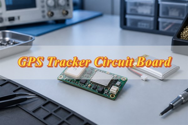
A GPS tracker circuit board receives satellite signals, processes location data, manages its power states, and sends selected information through a wireless connection. Its three main functional groups are the GNSS and antenna path, the controller and memory, and the power and communication circuits.
The exact configuration follows the product. A vehicle tracker may need input-transient protection and a backup supply, while a battery-powered pet tracker places more pressure on size, weight, charging, standby current, and antenna orientation.
Where Are GPS Tracker Circuit Boards Used?
GPS tracker circuit boards serve vehicles, assets, wearables, industrial equipment, and shipments, but the application changes what the board must withstand and how it should be tested.
- Vehicle trackers: vehicle power, continuous communication, and backup operation make input protection, power switching, interface design, and antenna position important.
- Asset trackers: long standby periods, intermittent coverage, and nearby metal increase the importance of low-power control, data storage, antenna placement, and mounting method.
- Pet wearables: size, weight, wearing orientation, water resistance, and charging requirements affect component density, battery space, antenna clearance, and sealing.
- Industrial trackers: temperature, vibration, electromagnetic interference, and service life influence component selection, connection reliability, protection, and test coverage.
- Shipment monitors: condition logging and delayed uploads require suitable sensors, memory capacity, reporting logic, and a power budget for periods without coverage.
Product safety, radio approval, cybersecurity, and traceability still depend on the sales region and intended use; they should be identified before the design is frozen.
What Are the Requirements for GPS Tracker Circuit Board Design?
Before design or quotation, confirm the inputs that determine the board outline, radio architecture, power budget, manufacturing route, and validation scope. The following information prevents late changes from being discovered only after a prototype is assembled:
- Mechanical limits: provide the target product dimensions, board outline, enclosure model, mounting points, connector access, battery position, and available antenna clearance.
- Markets and networks: identify the sales regions, cellular or other communication technologies, frequency bands, SIM approach, roaming needs, and any required fallback link.
- Location and reporting behavior: state when the product needs a position, when it needs to upload, whether those intervals differ, and what it should do when a fix or network connection is unavailable.
- Battery target: provide the battery type and capacity, required operating life, charging method, allowed charging time, replaceability, and expected low-temperature use.
- Antenna approach: identify the GNSS and communication antenna types, internal or external installation, cable or connector requirements, intended device orientation, and nearby metal.
- Environment and production scope: specify temperature, moisture, vibration, ingress protection, coating or potting, compliance needs, programming responsibility, test coverage, quantities, and records required with each build.
How Does GPS Tracker PCB Layout Affect Positioning and Wireless Communication?
GPS tracker PCB layout preserves the conditions that a weak GNSS signal needs, while limiting noise and coupling from digital, power, and communication circuits. The layout should be reviewed as part of the final mechanical and radio system, not as an isolated 50 Ω trace.
- Antenna and enclosure: determine the antenna position before dense component placement. Clearance, ground plane, device orientation, the battery, cables, fasteners, and nearby metal can change reception, so compare the open board with the production-intent enclosure.
- RF path and reference ground: calculate the 50 Ω geometry from the released stackup and review the full path through pads, connector launches, vias, matching parts, and any cable. Keep the reference plane continuous, and keep noisy routing outside the antenna keepout.
- GNSS and communication coexistence: compare receiver behavior with transmitters, high-current loads, clocks, and switching converters active and inactive. If reception changes, separate RF coupling from supply disturbance before choosing separation, filtering, shielding, grounding, or power-path changes.
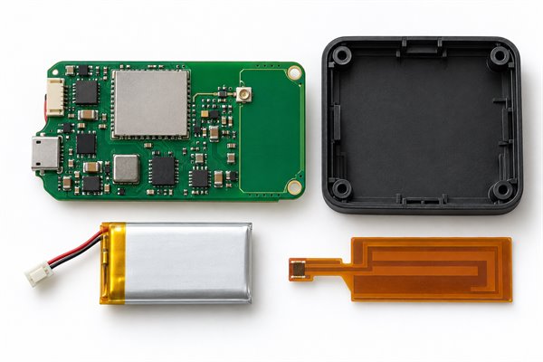
A PCB antenna design review should include the antenna datasheet, released stackup, placement and keepouts, matching network, enclosure model, battery and cable locations, and the planned comparison tests. PCB layout can protect reception conditions, but positioning accuracy also depends on the receiver, antenna, firmware or algorithm, sky view, multipath, movement, and operating environment.
How Can GPS Tracker Circuit Board Design Balance Size and Battery Life?
Balance size and battery life by treating energy consumption, peak-current delivery, and physical space as related but separate design constraints. A tracker may meet an average-current target yet still reset when the cellular modem transmits, especially at low battery voltage or low temperature.
- Separate location and upload schedules: a product may acquire positions frequently but upload them in batches, or wake only for event-driven reports. Model the two intervals independently because GNSS acquisition and network transmission create different loads.
- Include time-to-fix and network retries: weak sky view, expired assistance data, registration delays, coverage loss, and retry logic keep circuits active longer than a typical datasheet example.
- Measure standby as a system state: account for regulator quiescent current, charger leakage, fuel gauge, wake sources, sensors, level shifters, indicators, and unintended I/O back-power paths.
- Verify peak supply separately: test the battery, protection circuit, regulator, copper path, connector, and local capacitance at the lowest expected battery voltage while the maximum agreed loads operate.
Average current = sum of (current in each operating mode × time in that mode) ÷ total operating time. This calculation assumes that the listed modes do not overlap. If GNSS, processing, sensors, and transmission can run together, measure or calculate those combined states instead of adding overlapping times twice.
Use measured prototype current and real state durations to replace early estimates. Before reducing the outline, reserve antenna clearance and ground, battery volume, manufacturable component spacing, thermal and current paths, connector access, and programming or fixture contacts. Rigid-flex or a daughterboard can help in some enclosures, but neither replaces these basic space requirements.
What Should You Verify During GPS Tracker Circuit Board Prototyping?
Prototyping answers whether the design meets the product requirements and which RF, power, mechanical, and recovery risks have been verified. It is a design-learning stage; later production tests should confirm that each manufactured board matches the approved design and limits rather than repeat every development experiment.
- Compare the open board with the enclosed product: use the same antenna, battery, cables, mounting surface, and orientation to identify detuning, shielding, or coupling introduced by assembly.
- Run GNSS while the radio transmits: compare defined receiver indicators before, during, and after communication activity to separate coexistence problems from normal reception variation.
- Test at low battery voltage: reproduce acquisition, network registration, and transmit bursts near the lower operating limit and watch for voltage droop, resets, corrupted data, or delayed recovery.
- Measure real sleep current: use production-intent firmware, wake sources, sensors, charger, fuel gauge, and interfaces; confirm that the product enters and leaves each low-power state as intended.
- Interrupt location and network service: check how the tracker stores records, limits retries, recovers time and connectivity, and resumes reporting when service returns.
Keep the hardware and firmware revisions, configuration, test conditions, results, failures, and approved changes together. That record defines which prototype is approved and what must remain controlled during pilot and repeat production.
What Are the Steps in the GPS Tracker PCB Assembly Process?
Assembly should reproduce the approved RF, power, component, programming, and test configuration without unapproved changes. Tracker-specific controls matter most around radio modules, RF matching parts, antenna connections, firmware identity, and protective processing.
- Review the release package. Cross-check PCB data, stackup, approved BOM and alternates, placement and assembly drawings, antenna and coax requirements, programming package, device-ID method, and test limits; close open questions before the build starts.
- Confirm components. Verify the exact GNSS and communication modules, RF filters and matching values, crystals, power parts, antenna connectors, and approved substitutions, along with package, storage, moisture sensitivity, and traceability requirements.
- Fabricate and test bare boards. Build the released material and stackup, control specified impedance, and verify dimensions, finish, solder mask, continuity, and isolation before assembly.
- Print solder paste and inspect it. Use the approved stencil and paste process, then perform SPI when specified so insufficient, excessive, or misaligned deposits are found before components are placed.
- Place and reflow components. Confirm orientation and critical RF-part values before reflow, use the approved profile, and complete any second-side or through-hole operations in scope.
- Inspect and complete special assembly. Apply visual inspection and AOI after reflow, and X-ray hidden or bottom-terminated joints when required. Assemble antenna connectors, coaxial cables, or external antennas to the agreed workmanship and handling requirements.
- Program, identify, and test. Link the controlled firmware and module configuration to the serial number or device ID, run the agreed board tests, and retain results with the batch record.
- Protect and release the build. Mask connectors, test points, pressure vents, and antenna areas before coating or potting. Review substitutions, defects, rework, yield, programming records, and test coverage before pilot approval or repeat production.
Compare custom PCB assembly services by change control, traceability, programming responsibility, test scope, and lot records.
How Are GPS Tracker Circuit Boards Inspected and Functionally Tested?
Inspection and functional testing answer whether a manufactured board matches the approved build and the project-specific acceptance limits. Visual, AOI, X-ray, electrical, programming, and functional methods each cover different defects, so the test plan should state where each method is used and what constitutes a pass.
| Production Check | Defined Test Condition | Acceptance Basis |
|---|---|---|
| Standby current | Specified firmware state, supply voltage, wake sources, interfaces, and disabled loads | Project limit plus correct entry into and exit from the defined low-power state |
| Transmit power supply | Specified battery or bench voltage and agreed modem operating mode | Allowed current and voltage variation with no reset, data loss, or abnormal recovery |
| GNSS response | Defined antenna connection and either a controlled signal source or a documented outdoor condition | Project-specific receiver response; results from controlled and outdoor methods are not treated as directly interchangeable |
| Communication | Defined module configuration, SIM or network setup, command sequence, and upload scope | Expected module response and completion of the agreed connection or data-transfer check |
| Programming and traceability | Released firmware, configuration, device-ID method, fixture, and database or record format | Correct version and identity with a stored pass/fail result linked to the board or batch |
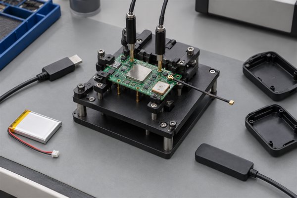
Set the limits, sampling plan, retest rules, and record format for the actual product; generic current, voltage, or GNSS limits are not reliable substitutes. Inspection criteria should also be agreed before production. When J-STD-001 or IPC-A-610 is specified, the purchase or assembly documentation should identify the required revision and class together with any project-specific workmanship requirements.
What Affects GPS Tracker Circuit Board Prototyping and Assembly Cost?
Compare quotations against the same PCB, component, assembly, programming, testing, and order requirements. The following items have the greatest effect on prototype and production cost:
- PCB construction: layer count, material, stackup, controlled impedance, board outline, and rigid-flex features change fabrication work. Use the simplest construction that still meets the RF, power, routing, and mechanical requirements.
- Components: module pricing, minimum order quantities, availability, lifecycle risk, and traceability affect material cost and schedule. Provide exact part numbers and clear substitution rules.
- Assembly complexity: fine-pitch packages, bottom-terminated parts, double-sided assembly, antenna cables, and mixed processes add setup, inspection, and rework requirements.
- Programming and testing: firmware handling, fixtures, test coverage, cycle time, and data records can add one-time development cost and recurring production work. Specify interfaces, limits, sampling, and retest rules before quoting.
- Quantity and added processes: order volume, coating, potting, enclosure work, labeling, packaging, and logistics affect setup and unit pricing. Separate one-time or stage-specific charges from recurring costs.
For a fair comparison, confirm whether critical modules, antenna accessories, programming, functional testing, protective processing, and production records are included in each quotation.
Why Choose EBest Circuit as Your GPS Tracker Circuit Board Manufacturer?
EBest Circuit supports the project from design review through repeat production, helping customers reduce handoff gaps and keep the approved build under control.
- Reduce late redesigns: receive a DFM issue list and open-items list covering the stackup, footprints, RF path, component availability, assembly access, programming, and testability before fabrication.
- Start with a clearer manufacturing scope: align the PCB data, BOM, antenna requirements, enclosure constraints, programming responsibility, test coverage, quantities, and records before the build begins.
- Control component substitutions: use an approved BOM with defined alternates and approval rules so critical GNSS, communication, RF, and power parts do not change without review.
- Keep repeat orders consistent: link the PCB revision, assembly data, firmware package, module configuration, device-ID method, and agreed test records from prototype through production.
- Match construction to the product: select standard FR-4, multilayer, high-frequency, flexible, or rigid-flex options according to the RF, space, and mechanical requirements instead of paying for unnecessary complexity.
- Receive agreed quality evidence: agree on inspection, programming, functional-test, and batch records in advance so your receiving and engineering teams know what evidence will accompany the order.
- Simplify supplier qualification: review EBest Circuit’s listed IATF 16949, ISO 9001:2015, ISO 13485:2016, AS9100D, REACH, RoHS, and UL information, then confirm the applicable legal entity, site, scope, and current revision for your program.
What Files Are Needed for a GPS Tracker Circuit Board Quote?
You can request an initial assessment before every manufacturing file is complete. Send the target product size, main GNSS and communication modules or required functions, antenna approach, prototype and forecast quantities, and target timing. EBest Circuit can identify the missing inputs and whether design review, prototyping, or assembly is the appropriate next step.
For a complete manufacturing quotation, provide the released production data where available:
- PCB package: Gerber, ODB++, or IPC-2581 data, drill files, board outline, fabrication drawing, stackup, and controlled-impedance requirements.
- Assembly package: approved BOM and alternates, centroid or pick-and-place file, assembly drawings, polarity notes, and antenna or cable assembly details.
- Programming and test package: firmware and configuration files, programming method, device-ID rules, test conditions, pass/fail limits, sampling, and required records.
- Commercial scope: prototype and forecast quantities, target schedule, consigned materials, coating or potting, enclosure or labeling work, packaging, and shipping destination.
More complete files produce a firmer price and schedule, but missing information does not prevent the first review.
FAQ About GPS Tracker Circuit Boards
Q1: What is the difference between GPS and GNSS on a tracker circuit board?
A1: GPS is one satellite navigation system, while GNSS is the broader term for receivers that may use several constellations. Confirm the bands and constellations supported by both the receiver and antenna.
Q2: Should a tracker use an active or passive GNSS antenna?
A2: A passive antenna uses no LNA power but needs a low-loss RF path and suitable placement. An active antenna can offset path or cable loss, but it requires bias power and compatible gain. Make the choice with the receiver requirements and final enclosure in view.
Q3: Why can GNSS reception become worse after the tracker is assembled?
A3: The battery, cables, coating, nearby metal, mounting surface, and user’s body can detune or shield the antenna. Switching converters and transmit radios can also reduce receiver margin, so compare the open board with the production-intent device.
Q4: Does a GPS tracker circuit board always need four layers?
A4: No. Layer count depends on routing density, RF reference planes, power distribution, EMC risk, board size, and package choice. Use the simplest stackup that still provides continuous return paths, required impedance, and manufacturable clearances.
Q5: How should battery life be estimated before production?
A5: Build a mode-based energy budget, then replace early current and timing assumptions with prototype measurements. Include acquisition time, network registration and retries, standby loads, regulator loss, temperature, and battery aging.
Q6: Can board-level testing guarantee tracker accuracy in the field?
A6: No. Board tests can verify assembly, power, interfaces, programming, and defined receiver responses. Accuracy still depends on the antenna, enclosure, firmware or algorithm, mounting, movement, sky view, and operating environment, so finished-device and field validation remain necessary.
A reliable tracker depends on more than a working GNSS module. Antenna and enclosure integration, peak-current stability, controlled component choices, repeatable assembly, and project-specific testing must support the same product requirements from prototype through production.
Ready to request a GPS tracker circuit board quote? Send your available design files, target functions, quantities, and test requirements to sales@bestpcbs.com. EBest Circuit will review the information, identify missing inputs, and recommend the next step for design review, prototyping, or assembly.