PCB manufacturing PCB manufacturing
Home > Blog

router PCB

Network Device PCB Manufacturing & Assembly Services | Reliable Quality Control
Tuesday, October 13th, 2026

Network device PCB manufacturing and assembly services take a released router, switch, access point, or gateway design through fabrication, sourcing, assembly, inspection, and agreed board-level tests. Buyers need evidence that the bare board matches the stackup and geometry, the parts and ports are assembled correctly, and the finished PCBA produces repeatable power and communication results under the specified test conditions.

At EBest Circuit, one engineering team coordinates those stages for prototypes and volume orders. We raise build, BOM, connector, mechanical-fit, programming, and test questions before production, then carry the approved configuration and acceptance requirements into repeat orders.
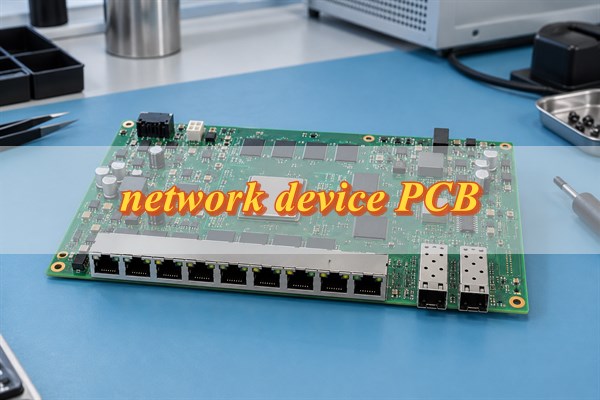
Network device PCB manufacturing and assembly for routers, switches, access points, and gateways

Are you worried about your network device PCB project?

» Will the board meet the released stackup, impedance, connector, and mechanical requirements?

» Can dense packages, multiport connectors, PoE parts, and wireless hardware be assembled consistently?

» Will prototypes and production units pass the same agreed power and communication checks?

EBest Circuit provides PCB manufacturing, sourcing, assembly, inspection, and production-transfer support for network equipment boards.

  • Review the build before fabrication: compare PCB data, stackup, BOM, connector geometry, mechanical constraints, and test access; return open questions before release.
  • Control board-specific risks: match checks to controlled-impedance features, hidden joints, port alignment, PoE paths, shields, and antenna connectors when applicable.
  • Define evidence before production: agree on inspection points, board-level tests, acceptance criteria, and comparison records.

Ready to start your network device PCB project? Send your available files, quantities, and test requirements to sales@bestpcbs.com.

What Is a Network Device PCB?

A network device PCB is the bare board that connects processing, memory, power, data-interface, and control circuits. After components are soldered, it becomes a PCBA that can be programmed, inspected, and tested against the product's board-level requirements.

A router PCB may combine a processor, memory, Ethernet PHYs, and a wireless module; a network switch PCB may add repeated channels, magnetics, RJ45 connectors, SFP cages, and PoE circuitry. These differences change the stackup, assembly route, thermal behavior, and test setup.

Which Network Devices Use These PCBs?

Network equipment PCBs support devices that route, switch, bridge, transmit, or manage data. Each device type brings different manufacturing priorities.

  • Router PCB: Dense processors, memory, PHYs, power, and optional wireless areas need package-appropriate soldering, power-rail checks, and verified RJ45 or antenna-connector fit.
  • Network switch PCB: Repeated channels, RJ45 banks, SFP cages, and optional PoE circuits make port alignment, connector joints, heat paths, and test access important.
  • Wireless access-point PCB: RF modules, PoE input, shields, and antenna connectors require careful handling, correct seating, and enclosure clearance.
  • Industrial gateway PCB: Isolation, field I/O, protection parts, and robust connectors must match the intended installation and mechanical data.

Controlled impedance or lower-loss material is used only when the released channel design requires it. Data rate, trace geometry, connectors, loss budget, and environment determine the build.

What Do Network Device PCB Manufacturing and Assembly Services Include?

The service may cover bare-board fabrication or a coordinated PCBA build. The quotation should identify every purchased deliverable, including inspection and testing.

  • Engineering review: Check fabrication, assembly, BOM, mechanical, programming, and test inputs for one revision.
  • PCB fabrication: Manufacture the board to the approved stackup, material, finish, dimensions, tolerances, and controlled features.
  • Component sourcing: Purchase against approved manufacturer part numbers and raise supply or packaging issues before placement.
  • PCB assembly: Complete SMT and applicable through-hole work for the released package and connector mix.
  • Inspection and testing: Perform the checks and provide the records stated in the order.

Combining fabrication, sourcing, and network PCB assembly reduces handoffs while keeping acceptance criteria clear.

What Is Reviewed Before Network Device PCB Manufacturing and Assembly?

Pre-production review checks whether all files describe the same build. It returns open items to close before purchasing or tooling.

  • Revision and file consistency: Compare PCB data, drills, drawings, BOM, centroid data, assembly notes, and test files. Missing or conflicting files are listed against one revision.
  • Stackup and controlled features: Check layer order, material, copper, thickness, drilling, tolerances, and any impedance or coupon requirement. Replace a vague “high-speed” note with measurable data.
  • Footprints and assembly inputs: Compare designators, packages, polarity, paste needs, coordinates, and inspection access, especially around BGA, QFN, memory, and fine-pitch parts.
  • Connector and enclosure fit: Check RJ45 bodies, SFP cages, shields, antenna connectors, heat sinks, mounting holes, slots, and board edges against front-panel and enclosure data. This can expose an electrically correct footprint whose seating height or body outline prevents assembly into the chassis.
  • BOM and change control: Verify manufacturer part numbers, values, packages, alternatives, and supply concerns. Any material, component, or engineering change requires customer approval before release.

How Is Quality Controlled During Network Device PCB Manufacturing?

Bare-board quality control verifies the PCB against released fabrication data. Useful evidence identifies the checked feature and the represented order or lot.

Check object Control or inspection method Result and available evidence when agreed
Material and stackup Verify laminate, copper, layer order, thickness, and finish Finds build mismatches; material or traveler records can identify the lot
Controlled impedance Control stackup and geometry; measure a coupon when ordered Compares the coupon with the specified range; a coupon or TDR record can be retained
Inner layers Use applicable AOI before lamination Finds opens, shorts, spacing defects, and imaging anomalies before burial
Drilling and registration Inspect drill position, registration, slots, and outline Finds offsets affecting vias, connectors, mounting, or chassis fit
Hole copper and plating Monitor plating; use measurements or microsections when specified Reveals inadequate plating, voids, or sampled structural defects
Finished circuitry Test against the fabrication netlist Finds opens and shorts; results or a lot summary may be supplied
Mechanical interfaces Measure agreed port, hole, slot, and board-edge features Confirms the geometry defined for connectors and the enclosure

Inner-layer AOI does not replace final electrical testing, and an impedance coupon does not prove Ethernet throughput. Buyers should specify required shipment records in the RFQ.
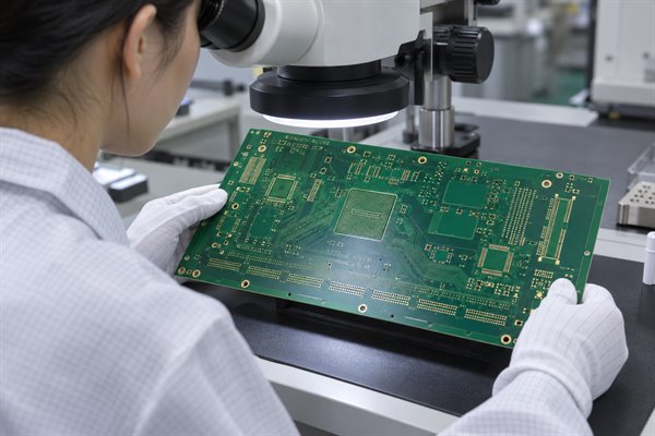
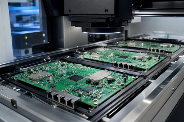
Bare network device PCB inspection and fabrication quality control

How Are Network Device PCBs Assembled?

Network device PCB assembly follows a sequence matched to dense packages, multiport connectors, thermal mass, and handling needs.

  • Verify materials: Match part identity, package, quantity, polarity, moisture condition, and consigned items to the released BOM. Resolve discrepancies before line loading.
  • Print solder paste: Use a stencil suited to fine-pitch parts, QFNs, BGAs, exposed pads, and larger joints. Check deposits before placement.
  • Place SMT parts: Load the approved program and confirm first-off polarity, orientation, and position, with added attention around processors, switch ICs, memory, PHYs, and power sections.
  • Reflow the SMT side: Use a profile suited to board thermal mass and component mix, including bottom-terminated packages.
  • Assemble connectors: Fit RJ45 banks, SFP cages, shields, headers, and through-hole parts using the specified soldering method. Check orientation, seating, board-edge position, coplanarity, and solder fill.
  • Add hardware: Install specified heat sinks, thermal pads, shield covers, fasteners, and antenna connectors. Verify identity, contact area, and fastening.
  • Clean and release: Apply the agreed cleaning and handling requirements, protect exposed contacts and RF interfaces, and send the PCBA to its inspection plan.

How Are Network Device PCB Assemblies Inspected and Functionally Tested?

Inspection and testing move from workmanship to power, programming, interfaces, and recorded pass/fail evidence.

  • Paste and visible joints: Use SPI when specified, then AOI to check component presence, polarity, position, and visible solder features before functional test.
  • Hidden joints: Use X-ray on selected BGA, QFN, or bottom-terminated joints when required by package risk and the inspection plan. X-ray does not replace electrical tests.
  • Connectors and hardware: Check RJ45/SFP alignment, solder fill, shields, antenna connectors, heat sinks, fasteners, markings, and cleanliness.
  • Power-up: Apply the specified input and compare current, rails, reset, startup, and agreed PoE observations with defined limits. Stop abnormal units before further test.
  • Programming and identity: Load or verify approved firmware and configuration, then read back required checksums, serial numbers, or MAC data.
  • Ethernet ports: Use defined link partners to verify negotiation, indicators, and packet criteria. For multiport boards, specify every-port or sampled coverage.
  • SFP, PoE, and wireless: Use the approved module, load, fixture, or connection method. Define PSE/PD role, load, active cages, and expected module response.
  • Failures and records: Isolate failed units, record the failed step, and retest approved repairs. Reports identify procedure revision, tested functions, limits, and represented units or lots.

Production testing confirms the agreed board-level functions only. Maximum system throughput, EMC, wireless coverage, final-enclosure thermal performance, and environmental reliability still require product-level validation.
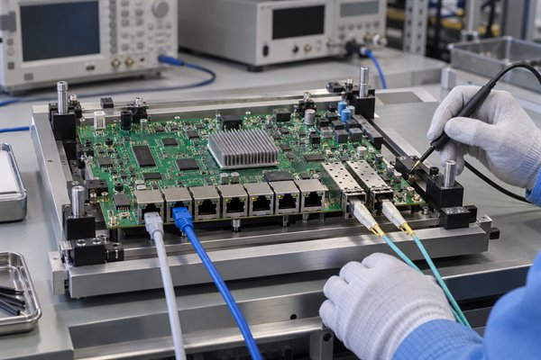
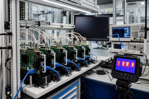
Network device PCB assembly inspection and functional interface testing

How Is Consistent Quality Maintained from Prototype to Mass Production?

A verified first article and frozen production baseline provide the reference for consistent volume quality. The transfer should make these controls visible:

  • First-article acceptance: Confirm PCB revision, components, connector fit, assembly details, programming, and agreed tests; close deviations before release.
  • Controlled production package: Release the stackup, materials, BOM and approved alternatives, assembly data, firmware, fixtures, inspection plan, test procedure, acceptance criteria, and packaging as one identified configuration.
  • Lot and unit traceability: When required, link each PCBA to its revision, relevant lots, firmware, serial or MAC data, and test record.
  • Nonconformance closure: Isolate failures, authorize rework, and retest affected functions. Feed repeated defects back into the process or work instruction.
  • Change revalidation: Assess changes to board material, critical parts, firmware, fixtures, or process conditions against the accepted baseline. Revalidate the affected features before the changed build becomes the next production reference.

What Affects Network Device PCB Manufacturing and Assembly Cost and Lead Time?

Cost and lead time depend on board construction, component supply, assembly route, test coverage, and how quickly open requirements are closed.

  • PCB construction: Layers, size, panel utilization, material, copper, vias, drilling, finish, tolerances, impedance, and records affect fabrication cost and time.
  • Component supply: BOM value, availability, minimum orders, alternatives, consigned parts, and packaging can set price and the earliest build date.
  • Assembly complexity: Fine-pitch or hidden-joint packages, two-sided placement, multiport connectors, shields, through-hole work, and thermal hardware add operations.
  • Programming and testing: Firmware, identity handling, fixtures, active ports, PoE loads, test duration, limits, and reports determine preparation and cycle time.
  • Schedule dependencies: Specified laminates, constrained components, unfinished fixtures, unresolved mechanical data, and late engineering changes can become the critical path even when fabrication capacity is available.

For a more comparable quote, separate prototype and volume quantities, identify fixed requirements and acceptable options, and state exactly which interfaces and records are needed.

Why Choose EBest Circuit as Your Network Device PCB Manufacturer?

EBest Circuit (Best Technology) brings 20 years of PCB and PCBA manufacturing experience to your network device project. From initial prototypes to volume orders, we help your team address manufacturing concerns, simplify purchasing, and verify board quality before shipment.

  • Free DFM review to reduce avoidable rework: Our engineers review your PCB files, stackup, BOM, and assembly requirements before production. Clear feedback helps you resolve manufacturing concerns early, saving time and reducing the cost of changes after fabrication begins.
  • Complete PCB and PCBA services to simplify sourcing: We coordinate PCB fabrication, component sourcing, assembly, programming, and agreed testing. Your team works with one manufacturing partner, reducing supplier coordination and keeping board and assembly requirements aligned.
  • Dedicated engineering support for faster decisions: Your project receives a dedicated engineering team to clarify technical questions and discuss practical manufacturing options. This helps engineers and purchasing teams move forward with a clearer understanding of requirements, scope, and cost.
  • Certified quality management to support supplier qualification: Our certifications include ISO 9001:2015, ISO 13485:2016, IATF 16949, and AS9100D. These provide a documented basis for evaluating our quality management practices and assessing their relevance to your project’s supplier requirements.
  • Inspection focused on critical network board features: Depending on your design, inspection can include X-ray checks of hidden BGA and QFN solder joints, connector alignment, and assembly checks around PoE circuitry, shields, and antenna connections. Targeted inspection helps identify defects that could affect board operation or final product assembly.
  • Testing planned around your product requirements: We coordinate programming and functional testing using your agreed procedures, firmware, fixtures, and acceptance criteria. This gives your team clearer evidence of board performance before shipment and supports more efficient product integration.

Send your Gerber files, BOM, quantities, and test requirements to **sales@bestpcbs.com** for a free DFM review and quotation. Our engineers will review your project and clarify the manufacturing and testing scope before production.

What Files Are Needed for a Network Device PCB Manufacturing and Assembly Quote?

Send the files that match the service you want quoted; unresolved details can be listed for engineering confirmation.

  • Bare PCB: Gerber or ODB++, NC drill, fabrication drawing, stackup if defined, quantity, and delivery location.
  • Assembled PCBA: Add the BOM with manufacturer part numbers, centroid or pick-and-place data, assembly drawing, and prototype or volume quantity.
  • Programmed or tested PCBA: Add firmware, programming method, identity-data requirements, active interfaces, fixtures or link partners, test limits, and required records.

Include an enclosure or front-panel drawing when connector height, board-edge position, mounting hardware, heat sinks, or cable clearance affects fit. We return missing or conflicting inputs as a short question list before finalizing the build scope and quotation.

FAQs About Network Device PCB Manufacturing & Assembly

Q1: Can prototype boards be assembled before production firmware is ready?

A1: Yes, prototype boards can be assembled before production firmware is ready. Define available checks, then verify final firmware, programming, and readback before release.

Q2: How can MAC addresses or serial numbers be kept unique during production?

A2: Use a controlled allocation file or generation rule with readback verification. Define the data format and programming interface so each identity can be confirmed.

Q3: Does every BGA or QFN require X-ray inspection?

A3: No, X-ray is not automatically required for every BGA or QFN. Coverage follows package risk and the inspection plan; it does not replace electrical or functional tests.

Q4: Can customer-supplied processors or network modules be used?

A4: Yes, customer-supplied processors and network modules can be used. Confirm identity, quantity, packaging, handling, shortage allowance, and traceability before the build.

Q5: What happens when a PCBA fails a production functional test?

A5: The failed PCBA is isolated and the failed step is recorded. Authorized repairs are retested, with final disposition recorded when required.

Q6: Can one PCBA be produced in several router or gateway variants?

A6: Yes, one PCBA can support several controlled variants. Define its BOM options, firmware, labels, assembly instructions, and matching test profile.

Ready to turn your released network device design into a repeatable PCB or PCBA? Email sales@bestpcbs.com with your files, quantities, and target service. We will return a focused engineering question list and a quotation defining fabrication, sourcing, assembly, inspection, testing, and records. This supports supplier comparison and prototype release.

You may also like

Router PCB Design, Prototyping and Manufacturing Services for Wi-Fi and Ethernet Products
Monday, August 17th, 2026

A router PCB must move data reliably while controlling RF coupling, power noise, heat and electromagnetic emissions inside a compact enclosure. EBest Circuit supports custom router PCB projects from engineering review and prototype fabrication through component assembly and repeat production. This guide explains the decisions that buyers and hardware teams should settle before requesting a quotation or releasing production data.

Router PCB design prototyping and manufacturing services for Wi-Fi and Ethernet products

Are you worried about delays or unexpected problems during router PCB design, prototyping and assembly?

  • Have the Ethernet, Wi-Fi, RF, power and return-path requirements been defined early enough to avoid late stackup changes and unnecessary board revisions?
  • Are the fabrication files, BOM and test criteria complete and aligned, or will missing details hold up the first build?
  • Can your manufacturing partner handle BGAs, RF components, connectors and approved substitutions while maintaining solder quality and consistent performance?

With 20 years of PCB and PCBA manufacturing experience, EBest Circuit supports router projects from design review through prototyping, assembly and production. Our one-stop service helps turn complex or incomplete requirements into a controlled, buildable manufacturing package.

  • Lock critical board requirements before fabrication: EBest reviews the proposed stackup, impedance table, Ethernet and RF reference routes, power-return paths, component footprints and DFM conflicts, then returns a clear issue list for customer confirmation.
  • Release one build-ready data package: EBest cross-checks Gerber or ODB++, drill data, the BOM, centroid files, drawings, firmware and measurable test limits so purchasing and production work from the same approved revision.
  • Control placement, soldering and verification: EBest confirms approved part numbers and substitutions, plans stencil and reflow requirements for BGAs and RF components, applies AOI and X-ray where appropriate, and checks agreed functions against documented acceptance criteria.

Ready to start your router PCB project? Send your design files, BOM, quantities and test requirements to sales@bestpcbs.com for an engineering review and quotation.

What Router PCB Design and Manufacturing Services Does Your Project Need?

The right service scope depends on how complete and proven your design is. A team with released Gerber files, a validated BOM and finished test software may need fabrication and assembly only. A project at schematic stage needs stackup planning, placement review, impedance definition, DFM feedback and a prototype test plan before production.

  • Design support: schematic review, component placement, stackup coordination, controlled-impedance planning and layout review.
  • PCB prototyping: small-batch fabrication for electrical, RF, thermal and enclosure validation.
  • PCB assembly: component sourcing, stencil preparation, SMT, through-hole assembly, rework and inspection.
  • Production support: panelization, test-fixture planning, traceability requirements and controlled engineering changes.

What Should Be Confirmed Before Starting a Router PCB Design?

Freeze the product interfaces and operating conditions before optimizing the board. The processor, Ethernet PHY, switch, memory, radio module or RF chipset, power architecture and antenna arrangement determine most routing and stackup decisions.

  • Network interfaces: record Ethernet speed, port count, magnetics arrangement, PoE requirement and connector choice.
  • Wireless functions: define Wi-Fi bands, MIMO channel count, antenna type, RF connector locations and coexistence requirements.
  • Mechanical limits: provide board outline, mounting holes, connector keepouts, enclosure height limits and airflow direction.
  • Power conditions: identify every input source, rail current, transient load, sequencing requirement and protection circuit.
  • Environment: state operating temperature, humidity, vibration, installation type and expected service life.

How Should Ethernet, Wi-Fi, RF and High-Speed Interfaces Be Laid Out on a Router PCB?

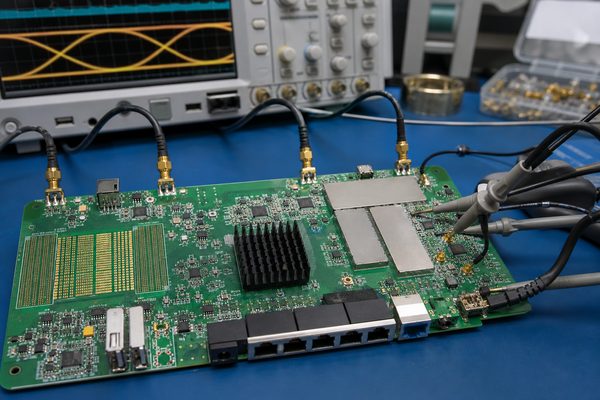
Each high-speed or RF interface needs a continuous return path and a routing rule based on its device documentation. Do not assign one generic trace width to Ethernet pairs, USB, memory and RF lines. Their target impedance, reference layer, loss budget and matching rules differ.

Router PCB RF and high-speed interface testing with oscilloscope probes

  • Ethernet pairs: keep each pair coupled, minimize skew, avoid plane splits and follow the PHY and magnetics reference layout for spacing and termination.
  • RF paths: keep transceiver-to-filter-to-antenna routes short, isolate them from switch nodes and crystals, and use the antenna vendor’s keepout rules.
  • Memory buses: place memory near the processor, control topology and length relationships, and avoid unnecessary layer transitions.
  • Reference transitions: add nearby return vias when a signal changes reference layers so the return current does not take a long detour.

How Do You Select the Stackup, Controlled Impedance and Materials for a Router PCB?

Select the stackup with the fabricator before final routing because dielectric thickness, copper weight and material properties set the impedance geometry. Layer count should provide practical signal layers, uninterrupted reference planes and adequate power distribution rather than simply meeting a board-thickness target.

For ordinary FR-4 multilayer work, EBest’s supplied capability table lists standard production from 1 to 10 layers, with high-Tg material required at eight layers and above; 10 to 32 layers require special evaluation. It lists standard 4/4 mil inner-layer line and spacing for 1/2 oz copper and standard 4/4 mil outer-layer line and spacing for 1 oz copper, with 3/3 mil treated as a special capability. These are manufacturing limits, not automatic design rules. A router PCB should use comfortable geometry wherever space permits.

Decision Confirm Before Layout Release Requirement
Layer stackup Layer order, dielectric thickness, copper weight and finished thickness Fabricator-approved stackup drawing
Controlled impedance Target, tolerance, trace type and reference plane Impedance table tied to net classes
Material Laminate family, Tg needs, loss needs and availability Approved material and substitution rule
Via structure Finished hole, aspect ratio and any blind or buried vias Drill table and fabrication notes

How Can You Control Signal Integrity, Power, Thermal and EMI Risks in Router Hardware?

Treat signal integrity, power integrity, heat and EMI as one coupled system. A noisy regulator can modulate a radio rail; poor return paths can increase emissions; excessive processor temperature can shift performance and shorten component life.

  • Power integrity: place decoupling capacitors at the intended device pins, keep high-current loops compact and verify rail droop during traffic bursts.
  • Thermal control: use thermal vias and copper spreading where appropriate, model enclosure airflow and measure component temperatures under sustained traffic.
  • EMI control: contain switching-current loops, preserve reference planes, separate sensitive RF areas and reserve practical shield-can boundaries when required.
  • Clock control: keep oscillators and clock routes away from antenna feeds, RF inputs and board edges; follow the clock source termination guidance.

What Files and Specifications Are Needed for Router PCB Prototyping?

A buildable prototype package must define the board, the assembly and the expected test result. Gerber or ODB++ data alone does not tell an assembler which component revision to buy or how to judge a programmed board.

  • Fabrication package: Gerber or ODB++, NC drill data, board outline, stackup, impedance table, fabrication drawing and readme.
  • Assembly package: BOM with manufacturer part numbers, centroid file, assembly drawings, polarity notes and approved substitutes.
  • Programming package: firmware image, programming tool requirements, connector or fixture definition and verification method.
  • Test package: power limits, expected rail values, interface checks, test-point map and pass/fail limits.

Cross-check revision identifiers before release. The fabrication drawing, Gerber or ODB++ data, BOM, centroid file, assembly drawing and firmware must all describe the same board revision. A shifted coordinate origin can misplace every component, an unapproved BOM alternative can change RF or power behavior, and a test instruction without measurable limits leaves the first build open to interpretation. Resolve these conflicts before material is ordered, then issue one dated package so purchasing, fabrication, assembly and test use the same baseline.

Which DFM Checks Should Be Completed Before Router PCB Fabrication?

DFM must check whether the released geometry can be fabricated, assembled and tested repeatedly. A basic clearance check is necessary but insufficient for a dense router board with BGAs, shields, fine-pitch RF parts and multiple external connectors.

  • Fabrication review: verify annular rings, drill-to-copper clearance, copper-to-edge spacing, solder-mask registration, aspect ratio and impedance coupons.
  • Assembly review: check paste apertures, BGA fan-out, component spacing, polarity visibility, shield-can access and rework clearance.
  • Panel review: confirm rail width, tooling holes, fiducials, breakaway strategy and connector overhang.
  • Test review: keep critical power, reset, programming and communication nodes accessible to probes or a fixture.

Classify each DFM finding by the action it requires. A copper clearance, annular-ring or solder-mask violation normally needs corrected production data; an impedance geometry question may require stackup confirmation and a revised trace rule; a connector overhang or shield-access issue may need mechanical approval. Record the affected layer, component or net, the proposed change and the person approving it. This prevents a fabricator’s local edit from becoming an undocumented design revision and makes the corrected package traceable for the next build.

What Does Router PCB Assembly Require for BGAs, RF Components and Connectors?

Router PCB assembly needs package-specific process control and a BOM that eliminates part ambiguity. BGAs hide their solder joints, tiny RF passives can be sensitive to placement and paste variation, and connector coplanarity affects enclosure fit.

Router PCB assemblies undergoing automated optical inspection

  • BGA process controls: review package pitch, pad definition, via-in-pad treatment, stencil apertures, moisture sensitivity and reflow compatibility before assembly.
  • RF component controls: verify the orientation of filters, matching components and crystals, and approve substitutions against footprint and RF performance rather than electrical value alone.
  • Connector controls: check RJ45, USB, SIM, coaxial and board-to-board connectors for seating, mechanical support, coplanarity and solder-joint access.
  • AOI inspection: use automated optical inspection to confirm polarity, placement, exposed solder fillets and visible paste-related defects, while recognizing that it cannot assess every joint beneath a BGA.
  • X-ray inspection: evaluate hidden BGA joints for bridges, opens, void patterns or inconsistent ball collapse when these conditions are included in the acceptance plan.
  • Functional verification: combine visual findings with orientation, seating-height and continuity checks, then apply the customer’s functional limits to confirm operation through the intended interfaces.

How Should a Router PCB Assembly Be Inspected and Tested?

Testing should progress from workmanship and shorts to power integrity, programming, interfaces and sustained functional load. A board that powers on is not yet a validated router assembly.

Router PCB functional traffic and thermal testing in production fixtures

  1. Inspect the assembly: use visual inspection and AOI for visible solder joints, polarity, missing parts and placement errors; use X-ray where hidden BGA joints require evaluation.
  2. Check unpowered nets: screen critical rails for shorts and compare resistance against an approved reference when available.
  3. Apply controlled power: use current limits, verify sequencing and measure each rail before full functional loading.
  4. Program and identify: load the approved firmware and record board revision, programmed version and traceability ID.
  5. Exercise interfaces: test Ethernet links at intended rates, wireless functions, USB, serial interfaces, LEDs, buttons and reset behavior as applicable.
  6. Stress the product: run sustained traffic and thermal checks in a representative enclosure and power condition.

How Do PCB Requirements Differ Across Wi-Fi Routers, 4G/5G Routers and Industrial Gateways?

The product category changes the dominant design risk even when the same manufacturing processes are used. Consumer Wi-Fi products emphasize RF coexistence, antenna integration and compact cost targets; cellular routers add modem power bursts, SIM interfaces and more RF paths; industrial gateways add wider environmental and protection requirements.

Product Primary PCB Concerns Validation Focus
Wi-Fi router MIMO antenna isolation, Ethernet routing, processor heat and compact placement Wireless throughput, Ethernet traffic, coexistence and enclosure effects
4G/5G router Modem current transients, multiple RF bands, SIM protection and RF connector placement Power bursts, cellular RF paths, antenna configuration and thermal load
Industrial gateway Input protection, isolation, rugged connectors, temperature range and service access Interface protection, long-duration load, environmental limits and maintainability

How Can a Router PCB Prototype Be Prepared for Stable Volume Production?

Convert prototype learning into controlled production data before increasing quantity. A stable pilot build requires more than correcting the faults found on the first samples.

  • Close every deviation: decide whether each rework wire, substituted part and manual adjustment becomes a documented design change.
  • Lock approved sources: identify alternates by manufacturer part number and validate critical RF, timing and power substitutions.
  • Define acceptance: convert engineering measurements into repeatable test limits and fixture instructions.
  • Review yield risks: examine defects by package, process step and board location before a larger build.
  • Control revisions: release one synchronized fabrication, assembly, firmware and test package.

Do not scale until the pilot build has a defined disposition. Separate design faults from process defects, component problems and test-fixture errors, then confirm that every accepted correction appears in the released data rather than only in rework notes. Compare defect counts and functional failures by board location or package type, confirm that critical alternates have been evaluated, and repeat the agreed tests on the corrected revision. Volume production should start from that approved baseline, with any later deviation routed through documented change control.

How Does EBest Manage Router PCB Prototyping, Assembly and Volume Production?

EBest uses one controlled release path from engineering review through fabrication, assembly and test coordination. The practical objective is to identify incomplete data and manufacturing risks before they become line-side questions.

The process begins with a review of the fabrication package, BOM, placement data and test requirements. Questions about stackup, impedance, material availability, component alternatives or panelization are returned for approval. After prototype assembly, inspection and customer-defined tests provide feedback for the next revision. When the design is ready to scale, the approved files, process notes and test criteria become the production baseline.

Customers receive decisions that can be traced to the released revision. Open items are returned as specific questions tied to the affected file, component or manufacturing feature instead of being resolved through undocumented shop-floor assumptions. Approved material choices, substitutions, panel details and inspection or test requirements are carried into the build package. For repeat orders, the same controlled baseline helps the customer identify what changed, what remained approved and which checks must be repeated before production continues.

Why Choose EBest Circuit for Router PCB Manufacturing Services?

Choose a supplier that can discuss board-level risks, not only quote layer count and quantity. Router products combine dense digital circuitry, RF paths, external connectors and power conversion, so early feedback can prevent expensive prototype spins.

  • Integrated support: fabrication, assembly and test-planning discussions can be coordinated within one project.
  • Manufacturing review: stackup, drill structure, fine geometry, panelization and assembly access are reviewed against the released data.
  • Prototype-to-production continuity: approved revisions, substitutions and process notes can be carried into repeat builds.
  • Clear engineering boundary: unverified capabilities and project-specific tests are confirmed before commitment.

The value is fewer unresolved decisions at the point of manufacture. One coordinated project path can expose a stackup conflict before impedance geometry is frozen, a BOM ambiguity before components are purchased, or an inaccessible test node before a fixture is built. The customer still approves design changes, substitutions and acceptance limits, while EBest keeps those decisions connected to the fabrication, assembly and test records used for the build. This is more useful than a quotation that confirms price and layer count but leaves technical assumptions unresolved.

FAQs About Router PCB Design and Manufacturing

Q1: How many layers does a router PCB need?

A1: There is no universal layer count. Select it from interface density, BGA escape needs, impedance geometry, continuous reference planes and EMC risk.

Q2: Does every router PCB require controlled impedance?

A2: Define controlled impedance for the relevant net classes. Most modern designs contain interfaces that require it; use the component guidance and a fabricator-approved stackup.

Q3: Can standard FR-4 be used for a Wi-Fi router PCB?

A3: Standard FR-4 is suitable for many router boards. Confirm it against frequency, route length, loss budget, temperature and the selected components rather than the product name alone.

Q4: What is the most common cause of a router PCB prototype delay?

A4: Incomplete or inconsistent release data is a frequent delay cause. Synchronize the BOM, centroid file, drawings, Gerber or ODB++ data, firmware and test instructions before release.

Q5: How are BGA solder joints checked?

A5: X-ray inspection is commonly used when hidden BGA joints require evaluation. Combine it with controlled assembly parameters and electrical testing.

Q6: Should antenna matching be finalized on an open prototype board?

A6: Final antenna verification should use the intended mechanical configuration. The enclosure, cables, shields and nearby structures can change antenna behavior.

Q7: What testing should be specified for router PCB assembly?

A7: Every production test needs a measurable pass/fail limit. Specify inspection, short checks, rail measurements, programming, Ethernet and wireless functions, peripherals and load conditions.

Q8: Can components be substituted during router PCB assembly?

A8: Components should be substituted only through an agreed approval process. RF, timing, power and high-speed parts may perform differently even when value and footprint appear compatible.

Q9: When is a router PCB ready for volume production?

A9: A working engineering sample alone is not sufficient. Close design changes, control sources and revisions, prove the intended production process and release test limits before scaling.

Q10: What should be sent for a router PCB manufacturing quotation?

A10: Send one synchronized fabrication, assembly and test package. Include stackup and impedance requirements, BOM, placement data, drawings, quantity, test scope and schedule needs.

How Can You Start a Custom Router PCB Project with EBest Circuit?

Start by sending a synchronized project package and a short description of the router’s interfaces, environment and test expectations. EBest can review the fabrication and assembly data, identify open engineering questions and confirm a practical prototype or production scope.

For custom router PCB design support, prototyping, assembly or manufacturing services, contact sales@bestpcbs.com. Include the target quantity, board revision, required interfaces and any controlled-impedance, material, component-sourcing or testing requirements.

You may also like