Photonic PCB manufacturing usually means building the electrical board that powers, controls, connects, and cools laser diodes, photodetectors, photonic integrated circuits (PICs), and optical modules. The quotation must separate standard PCB/PCBA work from specialist operations such as optical-waveguide fabrication, die attach, wire bonding, passive alignment, and fiber coupling.
EBest Circuit supports custom PCB fabrication, component sourcing, SMT and through-hole assembly, inspection, and the programming, electrical, or functional tests listed in the quotation. Before purchasing begins, our engineers compare the PCB files, stackup, fabrication drawing, BOM, placement data, assembly drawing, and requested tests. The returned question list identifies mismatched revisions, missing tolerances, unapproved material substitutions, inaccessible test points, and optical operations that require a separate supplier.
What Is a Photonic PCB, and Where Is It Used?
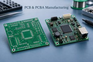
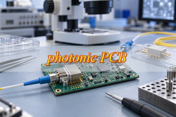
A photonic PCB is usually an electrical circuit board designed around optoelectronic components and their mechanical, thermal, and signal-integrity requirements. It may carry laser drivers, transimpedance amplifiers, photodiodes, optical-engine control circuits, or a PIC package while providing power distribution, grounding, control interfaces, and heat transfer.
Confirm whether the quotation covers a conventional electrical PCB or an electro-optical board with embedded waveguides. A conventional board routes power and electrical signals to packaged optical devices; an electro-optical board adds optical layers and requires a separate fabrication process, file set, and inspection plan.
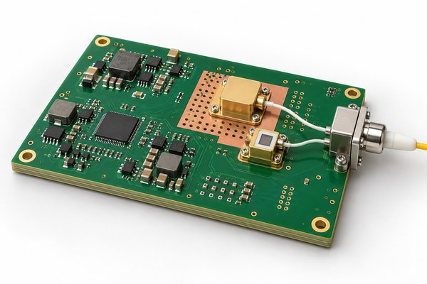
- Optical communications: Transceiver control, coherent-optics support electronics, optical engines, and board-level interconnect modules.
- Laser modules: Laser-diode drive, bias control, monitoring, protection, and heat spreading.
- LiDAR and sensing: Emitter control, detector front ends, timing, power conversion, and signal processing.
- Medical and scientific instruments: Optical sensing, imaging, spectroscopy, and measurement electronics.
- PIC packaging: Electrical fan-out and mechanical support around a separately packaged photonic device.
Record the selected architecture on the fabrication and assembly drawings. The quotation should then state who supplies the PCB, ceramic or metal submount, packaged optical device, waveguide layer, die attach, alignment, fiber coupling, and final optical test.
What Should You Consider When Designing a Photonic PCB?
Start photonic PCB design with the interfaces that can change optical-module fit or performance: board geometry, electrical channels, heat flow, component attachment, and test access. Release the board outline and datums, controlled-impedance nets, loss targets, thermal-interface drawing, component attachment method, and test-point or fixture requirements with the design package.
- Mechanical fit: Define the outline, finished thickness, datum scheme, cutouts, mounting holes, connector position, flatness or bow-and-twist requirement, and clearance to the housing or optical bench.
- Electrical performance: Identify controlled-impedance nets, return paths, reference planes, power integrity constraints, isolation needs, and the measurement method for high-speed channels.
- Thermal path: Calculate how heat travels from the laser, driver, or detector package through pads, copper, vias, submounts, interface materials, and the external heatsink.
- Attachment method: State whether each device is reflowed, selectively soldered, adhesively attached, socketed, press-fit, wire-bonded, or installed after the standard PCBA process.
- Inspection and test access: Reserve access for dimensional measurement, AOI or X-ray where applicable, electrical probes, programming, and functional fixtures.
Do not apply the tightest tolerance to every feature. Mark only dimensions that control socket engagement, optical-package location, heatsink contact, connector alignment, or enclosure fit; otherwise the board may become more expensive without improving module performance.
Which Materials and Stackups Are Right for Your Photonic PCB?
Select the material system from the electrical channel, heat load, mechanical envelope, and assembly temperature rather than from the photonic label alone. The table below separates common starting points by the problem they solve.
| Material or structure | Best-fit requirement | What to verify before release |
| High-Tg FR-4 multilayer | Control, power, monitoring, and moderate-speed digital routing | Confirm loss, thermal expansion, thickness stability, and assembly temperature for the actual design |
| Low-loss laminate | High-speed electrical channels with a defined insertion-loss budget | Use dielectric data at the relevant frequency and model the complete channel; low loss does not create an optical waveguide |
| Heavy-copper or localized copper structure | Current carrying and heat spreading around drivers or emitters | Check copper balance, manufacturable clearances, thermal interfaces, and resulting board flatness |
| Metal-backed PCB | Short thermal path to a chassis or cold plate | Review electrical isolation, machining, via options, and component-side routing limits |
| Alumina or aluminum-nitride submount | Localized device support where thermal or dimensional behavior justifies a ceramic | The ceramic may be a separate submount rather than the complete multilayer PCB |
| Hybrid board and submount assembly | Electrical routing combined with a localized optical or thermal carrier | Control the mechanical stack, attachment process, coplanarity, and supplier responsibility at every interface |
For a multilayer board, release the layer count, copper weights, dielectric materials, dielectric thicknesses, finished thickness, impedance targets, and any resin-fill or via-fill requirements as one controlled stackup. When a specific low-loss laminate is required, provide the manufacturer, grade, core and prepreg thicknesses, copper type, permitted substitute, and impedance target. The supplier should return the proposed build stackup and identify any material or thickness change before fabrication.
Approve the material only after the returned stackup shows each dielectric, copper weight, finished thickness, impedance construction, via-fill requirement, and allowed substitute. Any change that alters impedance, board thickness, heat flow, soldering temperature, or price should be listed for approval.
What Manufacturing Options Does Your Photonic PCB Need?
Choose each fabrication option from a named board feature: a socket cutout, heatsink area, bond pad, plated edge, or controlled-impedance channel. Put the required geometry, finish, tolerance, and inspection method beside that feature on the fabrication drawing.
- Controlled dimensions: Use fabrication drawings to identify critical outline features, slots, cutouts, datum-to-hole positions, finished thickness, and any localized flatness requirement.
- Thermal structures: Define filled and capped vias, thermal-via arrays, heavy copper, copper coins, or metal-backed constructions together with the intended heatsink interface.
- Bondable surface areas: Identify pads intended for soldering, wire bonding, conductive adhesive, or probing. ENEPIG may support soldering and compatible wire-bonding applications, but the finish, wire system, cleanliness, and bonding process still require qualification.
- Edge metallization: Provide geometry and acceptance criteria for plated board edges, castellations, or socket-contact surfaces rather than relying on a general edge-plating note.
- Controlled-impedance routing: Mark the nets, target impedance, reference layer, coupon requirement, and reporting expectation for high-speed electrical interfaces.
Replace “high precision” with measurable callouts for finished thickness, cutout position, hole-to-datum distance, edge finish, and local flatness. Put the nominal value and tolerance beside each controlled feature, then state whether it will be checked by optical measurement, CMM, gauge, coupon, or first-article inspection.
Can Your Photonic PCB Be Assembled with Optical Components?
Conventional PCBA processes can assemble the electronic portion of many photonic modules, but optical-device packaging must be scoped separately. SMT drivers, controllers, power devices, resistors, capacitors, connectors, and packaged photodiodes may fit a standard or mixed assembly route; bare dies, wire bonds, precision alignment, and fiber coupling may not.
- Included PCBA operations: Confirm stencil design, SMT placement, reflow, through-hole operations, connector seating, cleaning, AOI, X-ray, and electrical test requirements.
- Temperature-sensitive parts: Identify components with reflow, storage, moisture, cleaning, or handling limits and decide whether they are installed before or after the main thermal process.
- Die and submount attachment: Supply the die-attach or adhesive specification, cure profile, placement tolerance, material controls, and inspection criteria; capability must be confirmed for the exact package and process.
- Wire bonding: Define wire material and diameter, pad metallurgy, loop or pull requirements, contamination control, and acceptance evidence before assuming that a bondable finish alone is sufficient.
- Optical alignment and coupling: Treat active or passive alignment, lens installation, fiber attach, and optical-power verification as specialist operations requiring separate equipment, procedures, and acceptance limits.
Allocate responsibility before quotation: the PCB supplier may deliver bare boards or partially assembled PCBAs, while a qualified optical-packaging partner completes dies, alignment, coupling, and optical testing. Mark every optical operation as supplier-provided, customer-provided, subcontracted, or excluded so it cannot disappear inside a single PCBA price line.
How Quickly Can You Get a Custom Photonic PCB Prototype?
Prototype timing is determined by the longest confirmed dependency, not by a generic “rapid” label. Specialty laminate availability, stackup approval, controlled mechanical features, surface finish, consigned optical components, fixtures, and optical-packaging operations can each set the schedule.
- Release the board package: Provide Gerber or ODB++, NC drill data, fabrication drawing, approved stackup, impedance information, quantities, and critical mechanical requirements.
- Add the assembly package: Provide a BOM with manufacturer part numbers, centroid data, assembly drawings, polarity information, special handling notes, and approved alternatives.
- Close manufacturability questions: Resolve material substitutions, tolerance conflicts, surface-finish compatibility, panel support, thermal structures, and responsibility for optical operations.
- Approve evidence and schedule: Confirm the inspection, test, reports, delivery destination, and the date only after materials and outsourced specialist processes have been checked.
Ask the quotation to show five separate dates: material arrival, bare-board completion, PCBA completion, specialist optical work, and inspection or test release. This makes it clear whether a proposed shortcut changes only the schedule or removes required work.
How Can You Ensure Photonic PCB Quality and Reliability?
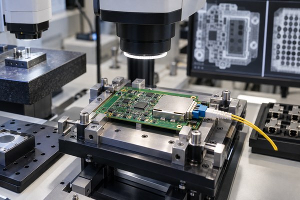
List every defect or function that can block shipment, then assign it a measurement or test and a shipment record. Bare-board electrical test cannot prove socket fit, wire-bond readiness, heatsink contact, optical alignment, or complete product function.
| Risk to control | Verification method | Evidence to request |
| Board does not fit the optical housing or socket | Dimensional inspection from the released datum scheme | First-article measurements for the named critical dimensions |
| Finished board is too warped for the thermal or optical interface | Bow, twist, or localized coplanarity measurement using the specified method | Measured result and acceptance limit for the controlled area |
| High-speed electrical channel misses its target | Controlled-impedance coupon and, when specified, channel measurement | Coupon result or agreed signal-integrity test record |
| Hidden solder joints contain process defects | Process control plus X-ray for specified BGA, QFN, or bottom-terminated packages | Inspection result tied to the lot or first article |
| Bonding or contact surface is unsuitable | Finish, cleanliness, packaging, and project-specific bonding qualification | Finish record and any agreed sample or bond-test result |
| Assembly does not perform its electrical function | Programming, electrical, or functional test using approved firmware and limits | Pass/fail record and traceability level defined in the quotation |
Before placing an order, ask the supplier to map each acceptance criterion to a method, sample plan, record, and owner. If optical power, insertion loss, or alignment is part of final acceptance, the quotation must also identify the equipment, fixture, reference condition, and party responsible for that measurement.
What Affects the Cost of Photonic PCB Manufacturing?
Cost rises when the design adds special materials, tighter controls, nonstandard processes, difficult assembly, or records that require dedicated fixtures and engineering time. Compare quotations only when they use the same material grade, quantity, assembly operations, inspection records, test work, packaging, and delivery terms.
- Material system: Specialty low-loss laminates, ceramics, metal backing, heavy copper, and hybrid constructions affect material price, availability, panel utilization, and processing.
- Stackup and geometry: Layer count, copper weight, finished thickness, aspect ratio, controlled impedance, small format, cutouts, and tight tolerances change fabrication difficulty.
- Special features: Filled and capped vias, copper coins, edge plating, bondable finishes, controlled-depth work, and localized mechanical inspection add process and verification steps.
- Assembly route: Fine-pitch packages, bottom-terminated components, mixed SMT/THT work, temperature-sensitive parts, consigned optical devices, and multiple attachment methods add setup and handling.
- Inspection and test: First-article measurement, X-ray, programming, custom fixtures, functional testing, special reports, and optical tests must be priced to the requested evidence.
- Quantity and schedule: Prototype setup, minimum material purchases, attrition allowance, panel usage, repeat-order learning, and expedited dependencies affect unit and total cost.
Request separate quotation lines for bare PCB, sourced materials, PCBA, fixtures, specialist optical operations, inspection, testing, and excess material. The breakdown reveals whether a lower price excludes work that another supplier included.
Why Choose EBest Circuit for Your Photonic PCB Project?
EBest Circuit applies 20 years of PCB and PCBA experience to a file-by-file preproduction review. Before purchasing, engineers compare the released PCB data, stackup, fabrication drawing, BOM, placement data, assembly notes, and test inputs. Open items are returned in one question list so the customer can approve changes before material is ordered.
- Free DFM review: Engineers review PCB data, stackup, fabrication notes, BOM, placement files, and assembly requirements so conflicts can be resolved before release.
- PCB and PCBA coordination: Fabrication, component sourcing, SMT, through-hole, mixed assembly, inspection, programming, and specified electrical or functional tests can appear in one line-item quotation.
- Prototype-to-volume continuity: Approved stackups, BOM decisions, process notes, first-article findings, and acceptance requirements can become the reference for repeat orders.
- Project-specific process review: Thermal structures, edge plating, special finishes, small board formats, fine-pitch packages, and consigned components are evaluated against the actual files rather than treated as universal promises.
- Inspection matched to risk: Dimensional checks, AOI, X-ray, electrical test, programming, and functional checks are selected according to the board features and agreed acceptance plan.
- Certificates available for supplier review: EBest Circuit lists ISO 9001:2015, ISO 13485:2016, IATF 16949, and AS9100D. Buyers can request the current certificate files and compare the named holder, manufacturing site, covered activities, and expiration date with their approved-supplier requirements.
For projects that also need die attach, wire bonding, optical alignment, fiber coupling, or embedded optical waveguides, the quotation marks each operation as included, customer-provided, subcontracted, or excluded and names the inspection or test record required for acceptance.
What Do You Need to Request a Photonic PCB Quote?
For a comparable quotation, submit the same PCB revision, BOM, quantity, supply model, optical-operation split, inspection records, test requirements, packaging, and delivery location to every supplier. List any missing optical or mechanical input as an open item instead of allowing each supplier to price a different assumption.
- PCB production data: Gerber or ODB++, NC drill files, fabrication drawing, netlist when available, stackup, impedance information, quantity, and delivery location.
- Mechanical interfaces: Critical dimensions, datums, finished thickness, cutouts, flatness or coplanarity limits, enclosure or socket drawings, and heatsink-contact requirements.
- Material and finish requirements: Approved laminates, copper weights, via-fill or copper-coin details, surface finish, bond-pad notes, and permitted alternatives.
- Assembly inputs: BOM with manufacturer part numbers, centroid data, assembly drawings, polarity, customer-supplied parts, storage conditions, attachment methods, and temperature restrictions.
- Optical work ownership: State who performs die attach, wire bonding, alignment, lens or fiber installation, optical calibration, and optical-performance testing.
- Acceptance and records: Specify dimensional reports, impedance coupons, finish records, AOI or X-ray, programming, electrical or functional test, optical results, traceability, packaging, and first-article needs.
The supplier’s response should list included operations, exclusions, approved or proposed material substitutions, customer-supplied parts, inspection records, test fixtures, price lines, and the dated schedule for each production stage.
FAQs About Photonic PCBs
Q1: Can a photonic PCB be smaller than 10 × 10 mm?
A1: Yes, if the fabricator confirms a suitable handling and panelization route. Very small boards may need breakaway rails, carrier panels, special routing, or post-separation inspection. Ask the supplier to show how the board will be supported, separated, cleaned, and measured before approving the array.
Q2: Can a corner cutout be made to fit a PLCC socket or optical housing?
A2: Yes, when the mating drawing defines the controlled geometry. Provide the datum, cutout radius, finished thickness, contact position, and board-edge finish. The first-article report should measure the features that control engagement instead of relying on a visual fit check alone.
Q3: Does laser wavelength determine the PCB laminate?
A3: Usually not for an electrical board carrying packaged optical components. Electrical loss, temperature, dimensional stability, and assembly conditions normally drive the laminate. Wavelength becomes a direct material concern when light propagates through an integrated optical structure, which requires a separate optical-material and waveguide review.
Q4: Can wire-bond pads and SMT pads share one board?
A4: Yes, but the finish and assembly sequence must support both operations. The supplier needs the wire system, pad geometry, cleanliness limit, masking plan, and bonding qualification requirement before selecting the finish. The process plan should also protect the bond area from solder, flux, handling, and packaging contamination.
Q5: Can several laser diodes share one copper thermal structure?
A5: They can share it only after combined heat flow and temperature interaction are checked. Review device losses, spacing, copper geometry, interface resistance, heatsink conditions, and the permitted junction or case temperature. A prototype should verify the worst simultaneous operating condition, not only one emitter at a time.
Q6: How should exposed bond pads be packaged?
A6: Packaging should prevent contact, abrasion, particles, moisture exposure, and uncontrolled handling. Agree on trays, separators, protective covers, moisture barriers, or cleanliness controls according to the finish and subsequent bonding process. The packaging instruction should remain with the order so receiving personnel do not open or stack boards incorrectly.
Q7: Can customers consign laser diodes, PICs, or detector modules?
A7: Yes, subject to receiving, identity, storage, handling, quantity, and loss-allowance rules. Supply part numbers, lot information, packaging condition, moisture or ESD limits, and enough setup allowance for the approved process. The purchase order should define who approves damage disposition and what happens to unused or rejected material.
Q8: Can several photonic-module variants be included in one order?
A8: Yes, when each variant has controlled BOM, placement, firmware, labeling, and test records. Common panels or setup can reduce duplication, but the traveler and labels must identify each configuration. Do not mix variants if shared processing would make material traceability, programming, or pass/fail identification ambiguous.
Q9: What records can be requested with the shipment?
A9: Request the records listed beside each inspection and test item in the quotation. Examples include first-article dimensions, electrical-test status, impedance coupon results, inspection reports, programming logs, functional-test results, material or finish records, and lot identification. Confirm the report format and sampling level before ordering so the records are usable at incoming inspection.
Q10: What happens to unused customer-supplied optical components?
A10: The disposition should be agreed before the build. Define whether excess parts are returned, stored for a repeat order, scrapped with approval, or reconciled in a material report. Include the required return packaging, lot identification, storage period, shipping account, and authorization needed before any material is discarded.
Conclusion
A photonic PCB order is ready for quotation when the drawing controls board geometry and interfaces, the stackup controls materials and impedance, the BOM controls component identity, and the assembly and test documents assign each electrical and optical operation to an owner. These files give engineering a fixed build reference and let purchasing compare the same work across suppliers.
If you are preparing a prototype or production optical module, send the Gerber or ODB++ data, stackup, fabrication drawing, BOM, quantities, mechanical interfaces, attachment requirements, and inspection or test needs to sales@bestpcbs.com. EBest Circuit will return a DFM question list, line-item quotation, proposed stackup or process notes, included inspection and test records, exclusions, and a dated manufacturing schedule.