A PCB test fixture holds a printed circuit board in a repeatable position and connects selected nets, components or interfaces to test equipment. A well-designed fixture reduces manual probing, stabilizes electrical contact and makes the same test sequence practical across a production lot. It does not define the test by itself: coverage still depends on the board design, probe access, test program and acceptance limits.
What Is a PCB Test Fixture?
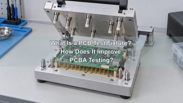
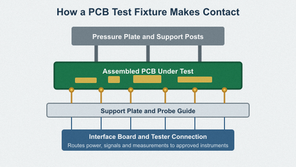
A PCB test fixture is a mechanical and electrical interface between a board under test and the instruments that stimulate or measure it. The fixture locates the board, applies controlled pressure and routes signals through probes, connectors or cables. A fixture may test a bare PCB, a partially assembled board or a complete PCBA, but those tasks require different hardware and test programs.
A bare-board electrical fixture checks continuity and isolation against a netlist. An assembled-board fixture can support in-circuit test (ICT), programming, boundary scan or functional test (FCT). Calling all of these a single “PCB tester” hides the most important question: what faults must the process detect?
How Does a PCB Test Fixture Work?
The operator or automated handler places the board against locating features. A press, vacuum plate or pneumatic mechanism then moves the board and spring probes into a controlled contact position. The test system applies power or test stimuli, measures the selected nodes and compares the result with the approved limits.
Reliable operation requires more than electrical continuity. Each probe must land on the intended pad with sufficient travel, the support plate must limit board deflection, and the interface wiring must preserve signal integrity and current capacity. The test program must also match the correct PCB revision.
What Are the Main PCB Test Fixture Parts?
PCB test fixture parts can be grouped by the job they perform: locating the board, making electrical contact, supporting the board, connecting to instruments and controlling the test cycle.
| Fixture part | Function | Common failure risk |
|---|---|---|
| Base, nest and alignment pins | Set the board position and orientation | Wrong datum, wear or reversed loading |
| Pressure plate and press posts | Apply contact force without loading components | Board bow, cracked components or uneven probe travel |
| Pogo pins and receptacles | Contact test pads, vias or connector points | Contamination, bent tips, wear or wrong probe style |
| Support plate | Limit deflection near dense probe areas | Unsupported zones and solder-joint stress |
| Interface board and wiring | Route test nodes to the tester | Crosstalk, excessive resistance or current overload |
| Interlocks and sensors | Confirm closure and safe operating conditions | Bypassed safety or incomplete engagement |
Types of PCB Test Fixtures
The correct type follows the test objective, board volume, node count, signal requirements and operator workflow. A bed-of-nails PCB test fixture provides many simultaneous contacts and is commonly used when repeatability and cycle time justify dedicated tooling.
| Fixture type | Best suited to | Main limitation |
|---|---|---|
| Manual clamshell fixture | Prototype, engineering validation and moderate volumes | Operator-dependent loading and cycle time |
| Pneumatic fixture | Higher-volume repeated tests with controlled actuation | Requires guarding, air supply and validated force |
| Vacuum fixture | Even board actuation across many probes | Seal design and board porosity affect operation |
| ICT bed-of-nails fixture | Network and component-level access | Requires DFT test points and dedicated programming |
| PCB functional test fixture | Power-up, I/O and behavior under defined conditions | Needs product-specific loads, interfaces and limits |
| Universal PCB test fixture | Reusable carriers or configurable low-node-count tasks | Usually less optimized than dedicated tooling |
A flying probe tester is different: it moves programmable probes between points and normally avoids a dedicated bed-of-nails fixture. That flexibility suits prototypes and changing designs, while fixed fixtures usually become more attractive as volume and repeated test time increase.
PCB Test Fixture vs Test Jig: What Is the Difference?
In electronics manufacturing, “fixture” and “test jig” are often used interchangeably. A useful distinction is that a fixture primarily locates, supports and interfaces the board, while a jig may also guide an operation or provide a simpler application-specific test setup. The name is less important than the documented function.
A purchase specification should identify the board revision, test coverage, actuation method, probe map, instrument interface, software ownership, cycle-time target, maintenance items and acceptance method. This prevents a PCB test fixture jig from being accepted only because the board physically fits.
ICT vs Functional Test Fixtures
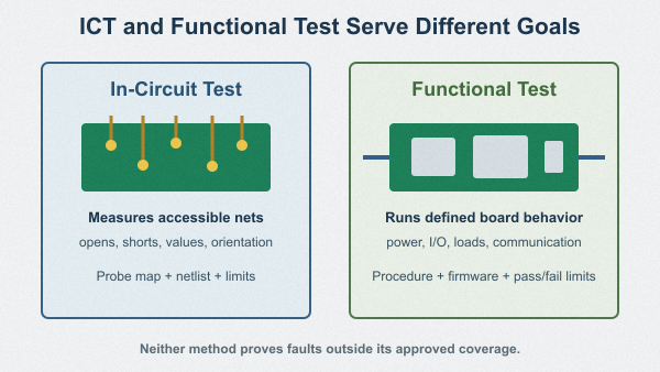
In-circuit testing examines electrical networks and component-related measurements through accessible nodes. It can identify faults such as opens, shorts, some wrong values, orientation errors and missing parts when the test method and access allow them. ICT does not prove that every product function works under its real operating conditions.
Functional circuit testing powers the assembly and checks defined behavior through connectors, loads, communication interfaces or simulated sensors. A PCBA functional test fixture may need controlled supplies, programmable loads, isolation, data communication and product-specific software.
| Question | ICT fixture | Functional test fixture |
|---|---|---|
| Primary objective | Find network and component-level manufacturing faults | Verify defined board behavior |
| Typical access | Test pads through pogo pins | Connectors, programmed I/O and selected probe points |
| Board state | Usually unpowered or powered under controlled test conditions | Powered and operating in a controlled test mode |
| Required inputs | Netlist, BOM, probe map, device models and limits | Functional procedure, firmware, loads, interfaces and pass/fail limits |
The two methods can complement each other. The required coverage should be assigned explicitly instead of assuming that one fixture will detect every possible defect.
What Does PCB Test Fixture Design Require?
PCB test fixture design begins with the test requirement and the released board data, not with the enclosure. The designer must know which nodes need access, which signals are sensitive, how much current each contact carries, where the board can be supported and which components must remain clear of pressure posts.
- Electrical inputs: netlist, test coverage, expected values, power rails, current limits, interface pinout and instrument requirements.
- Mechanical inputs: board outline, thickness, tolerances, datum holes, keepouts, connector locations, component heights and panel condition.
- DFT inputs: test-point coordinates, pad dimensions, mask openings, probe side, no-probe zones and expected access percentage.
- Production inputs: target volume, cycle time, operator steps, barcode or traceability needs, repair route and expected fixture life.
- Change control: PCB revision, BOM revision, firmware version, test-program version and fixture drawing revision.
For FR4 PCBs, datum holes, board-edge clearance and test pads should be fixed before layout release. On multilayer PCBs, internal connections cannot be inspected visually, so netlist control and intentional test access become more important.
How Should Test Points Be Designed for a Bed-of-Nails Fixture?
Test points should provide a clean, repeatable landing surface without forcing probes onto fragile component leads or solder fillets. Exact pad size and spacing depend on the selected probe series, drill accuracy, board tolerance and fixture vendor rules, so they must be agreed before the PCB layout is frozen.
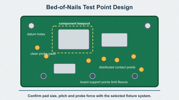
- Use stable mechanical datums and prevent 180-degree loading where the outline is symmetric.
- Keep mask openings and probe pads free from silkscreen, paste residue and nearby tall components.
- Distribute high probe-force areas and add support beneath the board to limit flexure.
- Separate sensitive analog or high-speed nodes from long unshielded fixture wiring.
- Define accessible ground references and power contacts with suitable current capacity.
- Reserve access for programming, boundary scan and debug only where the production test plan requires it.
Dense HDI PCBs often leave less room for dedicated test pads. Early DFT review may use connector access, boundary scan or selected functional coverage where full bed-of-nails access is not practical; the reduced coverage must be understood rather than hidden.
When Is a PCB Test Fixture Worth the Cost?
A dedicated fixture is justified when its setup cost is offset by shorter repeat test time, lower handling variation, better traceability or broader simultaneous access. The break-even point depends on fixture cost, test time saved per board, expected production quantity, product lifetime and the cost of escapes or false failures.
For early prototypes or frequently changing revisions, flying probe testing and bench functional tests can avoid premature tooling. For stable designs moving into repeated production, a manual PCB test fixture or automated fixture can reduce operator probing and support consistent data capture. The decision should include expected ECOs because a pad map or connector change can require fixture rework.
What Causes False Failures in PCB Fixture Testing?
A false failure occurs when the test reports a bad board even though the assembly meets the intended requirement. Intermittent contact is a common cause, but it is not the only one.
| Symptom | Likely fixture-related cause | Check |
|---|---|---|
| Failure moves between nodes | Dirty or worn pogo pins | Inspect tips, clean, cycle and replace by record |
| Failure changes with pressure | Uneven travel, board bow or poor support | Measure probe compression and inspect support points |
| One revision fails repeatedly | Fixture or program revision mismatch | Compare PCB, BOM, firmware and test-program versions |
| High-current rail drops voltage | Undersized contacts or interface resistance | Measure loaded voltage at the board, not only at the supply |
| Intermittent communication | Long wiring, ground reference or shielding problem | Review return paths, cable length and signal bandwidth |
Limits that are too tight can also create false rejects when instrument uncertainty, fixture resistance and component tolerance were not included. A known-good board is useful for setup checks, but it does not replace correlation against the approved specification.
How Do You Maintain a PCB Test Fixture?
Maintenance should be based on cycle count, contact performance and observed defects. Clean probe tips with a method approved for the probe material, remove debris from the board nest, check alignment features and replace damaged probes with the specified series and spring force.
Record probe replacement, fixture repairs, calibration or correlation checks, and the board revisions supported by the fixture. A universal PCB test fixture or reusable kit still needs configuration control; reusable hardware does not make every adapter or program interchangeable.
What Files Are Needed for Fixture-Based PCBA Testing?
A manufacturable board package and a test specification must arrive together. For fixture-based testing, provide Gerber or ODB++ data, drill files, fabrication drawings, stack-up, IPC-356 or another approved netlist, BOM, centroid data, assembly drawings and a clearly identified PCB revision.
The test package should add the test-point list and coordinates, expected readings, tolerance limits, power sequence, current limits, firmware and programming files, connector pinout, required loads, communication commands, pass/fail logic, expected cycle time and handling instructions. For our PCB assembly services, we review customer-defined electrical and functional test requirements against the released design and agreed production scope.
PCB Test Fixture FAQs
Is a PCB Test Fixture the Same as a Flying Probe Tester?
No. A fixed fixture uses dedicated contacts and mechanical tooling. A flying probe machine moves programmable probes and normally does not require a dedicated bed-of-nails fixture.
Can One PCB Test Fixture Test Different Board Revisions?
Only when the mechanical datums, contact locations, interfaces and test program remain compatible. Every revision change should be checked against the fixture drawing and probe map before production.
What Is Included in a PCB Test Fixture Kit?
A kit may include a base, press mechanism, interchangeable plate, probes, receptacles, wiring and an interface board. Contents vary, so the probe map, tester connection, software and acceptance test should be specified rather than assumed.
Does a Passing Fixture Test Guarantee a Defect-Free PCBA?
No. A pass confirms only the faults and operating conditions covered by the approved procedure. Environmental, long-term reliability, enclosure-level and untested functional defects require other controls.
How Can We Support PCB Assembly and Testing?
At EBest Circuit (Best Technology), we support SMT, through-hole and mixed PCBA builds from prototype through volume production. Our documented inspection and test resources include 3D SPI, AOI, X-ray inspection and functional testing. The applicable sequence depends on component packages, defect risk, customer test procedures and the agreed acceptance criteria.
Send the released PCB data, BOM, assembly package and test specification to sales@bestpcbs.com. We can review DFT access, assembly constraints and fixture-interface requirements with the manufacturing package. A production-ready PCB test fixture must remain aligned with the actual board revision, test program and measurable pass/fail limits.