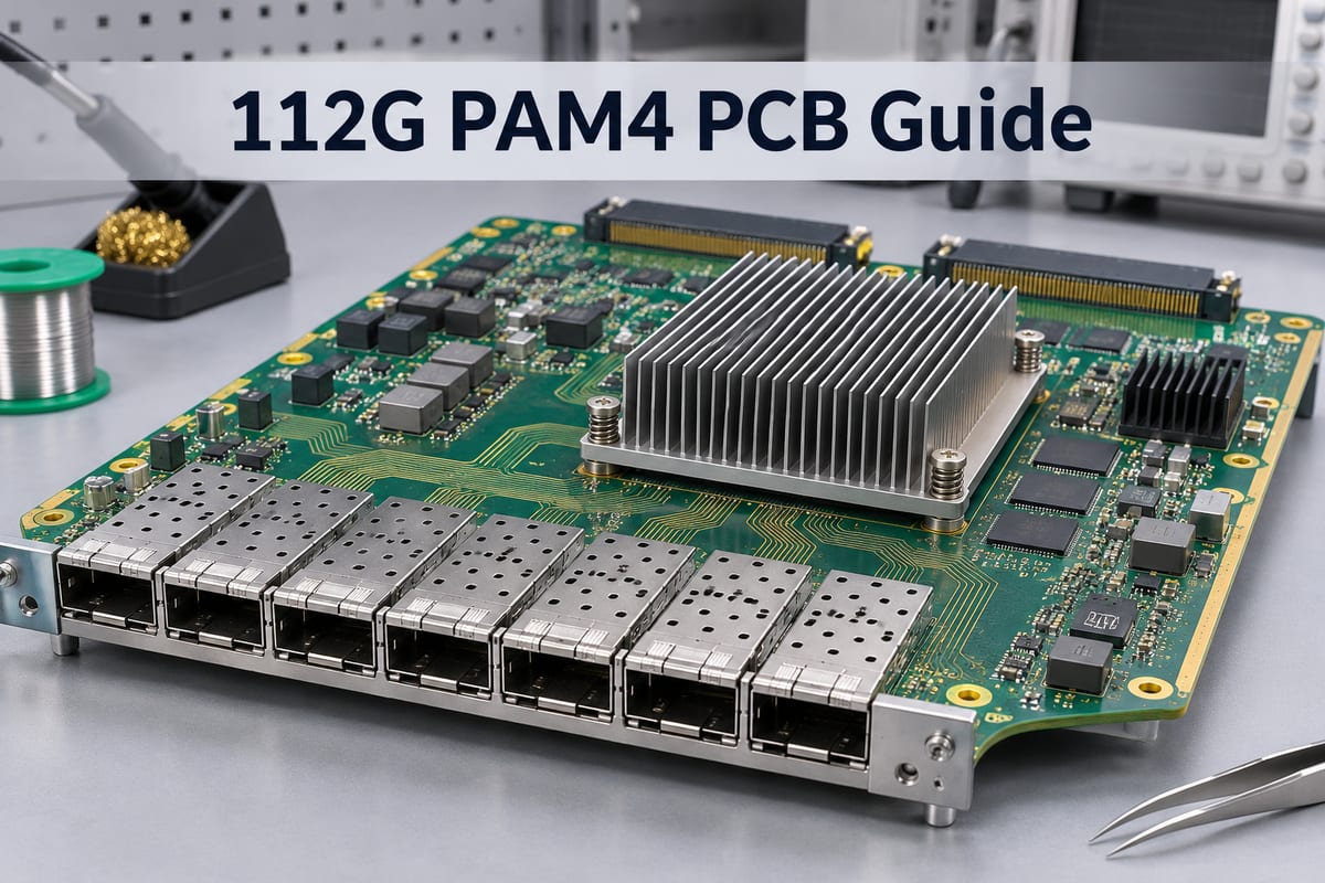
A 112G PAM4 PCB is not qualified by choosing a low-loss laminate and routing a nominal differential impedance. The complete electrical channel—package, traces, vias, connector launches and receiving circuitry—must meet the requirements of the selected interface. Start by identifying the exact lane rate, channel class and measurement reference planes. Then agree the stackup, models and manufacturing controls before releasing fabrication data.
This guide separates rate calculations from compliance limits and explains what engineers and PCB buyers should exchange. It does not prescribe a universal trace width, reach or backdrill depth: those depend on the actual construction and channel.
What Does 112G PAM4 Mean?
PAM4 uses four amplitude levels to encode two bits per symbol. Consequently, an illustrative gross rate of 112.0 Gb/s corresponds to 56 GBd. However, “112G” is also used as a technology-family label. A specific interface may use another exact rate; payload throughput additionally depends on coding and forward error correction.
Do not infer the electrical specification from a switch port’s aggregate data rate. A port can contain several lanes, and its optical and host electrical interfaces need not have identical lane arrangements. Record the governing specification and revision, SerDes mode, lane count and gross bit rate first.
Detailed Rate Parameters and Their Practical Meaning
For ideal PAM4 encoding, symbol rate equals gross bit rate divided by two. Symbol interval is the reciprocal of symbol rate; the Nyquist frequency is half the symbol rate. These calculations describe the signaling rate, not the required analog bandwidth of every device or instrument.
| Parameter | 112.0 Gb/s PAM4 example | 106.25 Gb/s PAM4 example | Design meaning |
| Bits per symbol | 2 | 2 | Four encoded amplitude levels |
| Symbol rate | 56 GBd | 53.125 GBd | Use the selected mode, not a rounded family name |
| Symbol interval | 17.857 ps | 18.824 ps | State whether timing budgets use symbol or bit intervals |
| Nyquist frequency | 28 GHz | 26.5625 GHz | A useful channel evaluation frequency, not a brick-wall bandwidth |
A reference clock frequency is a separate parameter. It must match the SerDes clock architecture, with the specified jitter integration band and operating conditions. It must not be substituted for the serial baud rate.
PAM4 vs NRZ: Lower Baud Rate, Tighter Vertical Separation
At the same gross bit rate, PAM4 halves the symbol rate relative to binary NRZ. That reduces the fundamental frequency burden, but introduces three eyes and smaller adjacent-level spacing. With the same ideal outer-level voltage span and equally spaced levels, adjacent PAM4 levels are separated by one-third of that span. Real receiver tolerance also depends on noise, linearity, jitter and equalization.
| Item | NRZ | PAM4 | Trade-off |
| Levels / bits per symbol | 2 / 1 | 4 / 2 | PAM4 carries more information per symbol |
| Symbol rate | 112 GBd | 56 GBd | PAM4 reduces the rate-related channel bandwidth burden |
| Nyquist frequency | 56 GHz | 28 GHz | Neither value alone specifies an instrument bandwidth |
| Eye structure | One eye | Three eyes | PAM4 requires level and eye-specific evaluation |
| Selection risk | Assuming bandwidth is sufficient | Assuming equalization fixes all impairments | Evaluate the complete specified link |
Define the Whole Channel Before Allocating Loss
Build a block list from transmitter reference plane to receiver reference plane. Include package models when required, every routed segment, layer transition, connector and applicable test fixture. Assign ownership of each model. A missing launch can make a simulation optimistic; including it in both a connector model and a PCB model can count its loss twice.
Insertion loss at one frequency is not a complete channel specification. Return loss, crosstalk, mode conversion and frequency-dependent behavior matter too. OIF defines multiple channel classes rather than one universal “112G reach.” Use the selected agreement and device requirements, not an unrelated backplane example, to establish the actual limits.
Select the Laminate Construction, Not Just a Material Name
Request the proposed laminate family, glass styles, resin content, cured dielectric thickness and associated electrical property data. Dk and Df depend on test method and conditions; values from different methods are not automatically interchangeable. The stackup used for simulation should match the construction that will actually be built.
Compare candidate constructions on modeled channel performance, fabrication availability and reliability requirements. A lower quoted Df is not by itself proof of a better finished channel. A thicker dielectric may permit wider conductors, but can change via geometry, board thickness and connector integration. Have the fabricator return the final impedance geometry for approval.
Include Copper Roughness and Finished Geometry
Conductor roughness contributes to high-frequency loss and can affect propagation. Specify the foil/interface information needed by the field solver and verify whether the model represents the relevant treated surfaces. Avoid mixing roughness parameters or models without understanding their definitions.
Finished trace width, thickness and cross-sectional shape are more useful than nominal artwork alone. Ask which geometry the impedance solver assumes and how process tolerances are evaluated. Do not claim a channel is robust simply because a single nominal stackup meets an impedance target.
Treat Connector Launches as Electromagnetic Structures
A connector’s headline data-rate label does not qualify its PCB footprint in a different stackup. Pads, antipads, reference-plane transitions, nearby ground structures and the connector itself form a coupled structure. Use a vendor-supported footprint and model for the relevant configuration, then reconcile the model boundary with the PCB extraction.
Before modifying a recommended footprint for routing convenience, identify whether it changes the modeled launch. A smaller pad may reduce one discontinuity while compromising assembly margin. Evaluate the electrical and manufacturing consequences together.
Control Via Stubs, Return Paths and Backdrill Boundaries
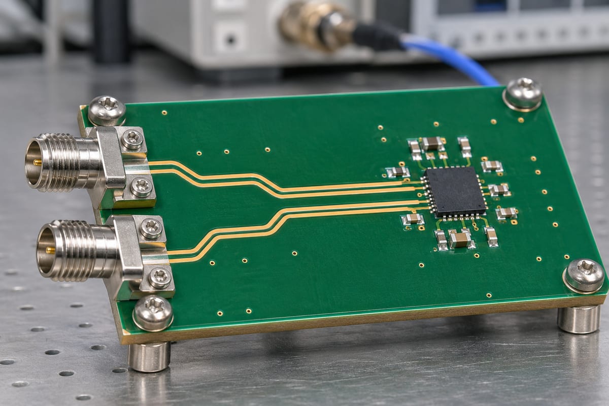
A layer transition must preserve a suitable signal and return-current path. Analyze the via barrel, unused stub, pads, antipads and surrounding return structures together. A generic instruction to “add ground vias” is not a substitute for a configuration-specific model.
If backdrilling is required, provide drill side, target layer, keep-out requirements and an agreed residual-stub tolerance. Check the tolerance against board thickness, layer position and the fabricator’s process. Do not specify an impractical zero stub, or assume that every via needs backdrilling regardless of its electrical role.
Manage Pair Skew Without Creating a Different Problem
Match the relevant electrical path, including breakout and transitions, rather than only CAD centerline lengths. Local asymmetry, different reference environments and material effects can change delay. Tight meanders used to remove a displayed mismatch can introduce coupling and impedance disturbances.
For scale only, 0.5 ps is about 2.8% of a 17.857 ps symbol interval. This calculation is not an allowable-skew specification. Obtain the actual budget from the interface and device requirements, and distinguish intra-pair skew from lane-to-lane timing.
Keep Power Integrity and Reference Clock Requirements in Scope
A passive channel can be acceptable while the assembled system fails because of supply noise or clocking behavior. Follow the SerDes vendor’s power, decoupling and reference clock recommendations. Specify how clock jitter is measured; a single unexplained femtosecond number is not a transferable qualification.
Power integrity review and channel review should share physical constraints. Changing a reference plane, clearance or power distribution feature to solve one issue can affect the return path of another. Review such changes before the final extraction rather than after manufacturing release.
Correlate Models and Measurements at Matching Reference Planes
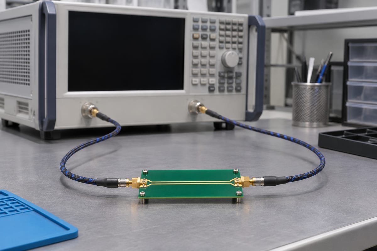
Record S-parameter port ordering, reference impedance, frequency range and de-embedding assumptions. Check that cascaded blocks use compatible definitions. The measurement fixture and launch must be included or removed consistently; otherwise measured and simulated results can disagree for reasons unrelated to the production trace.
For an active link, document transmitter settings, receiver equalization, operating conditions, test pattern and the relevant error/compliance method. A clear-looking eye screenshot alone does not establish compliance. A coupon also cannot prove that every populated connector and package transition behaves identically.
Manufacturing Release Checklist: Files, Owners and Acceptance
Release a controlled package rather than an email saying “112G capable.” Identify the stackup revision, final routing revision, approved launch geometry and models. Define who may approve material substitutions, copper changes, backdrill changes and CAM edits affecting the channel.
| Deliverable | What to specify | What it does not prove |
| Stackup and impedance drawing | Construction, finished geometry, target and tolerance, reference layers | Complete channel compliance |
| Via and backdrill definition | Layer transitions, drill side, residual-stub requirement, approval boundary | Acceptable connector launch without modeling |
| Channel model package | Ports, reference planes, versions, extraction assumptions | Correlation with hardware unless measured |
| Coupon and inspection plan | Structure represented, measurement method, acceptance criteria | Performance of every assembled system path |
| Change-control record | Substitution restrictions and named engineering approval route | That an unreviewed “equivalent” material is interchangeable |
Before approval, confirm: exact rate and channel class; complete block ownership; nominal and tolerance-aware extraction; no duplicated launch; agreed fabrication limits; documented test conditions; and a plan to resolve failed correlation. Electrical testing for shorts and opens remains necessary, but is not a high-frequency channel measurement.
FAQ
Is 112G PAM4 always 56 GBd?
Exactly 112.0 Gb/s gross PAM4 corresponds to 56 GBd. However, a product described as 112G-class can use a different exact rate in a selected protocol mode. Read the interface specification and device configuration before calculating Nyquist frequency or choosing a model and test setup.
Does a 400G port mean each PCB lane runs at 400 Gb/s?
No. Aggregate port throughput can be distributed across multiple electrical or optical lanes. Establish which side of the interface is being discussed and obtain its lane count, modulation and exact gross rate. The aggregate label alone does not define the PCB channel or a suitable SerDes component.
Can ordinary FR-4 be used for a short 112G channel?
Do not decide from the broad FR-4 label alone. Evaluate the actual construction, length, transitions and material properties against the applicable channel requirements. A short route is not automatically acceptable, and a low-loss material is not automatically necessary or sufficient for every design. Confirm the proposed stackup through analysis and validation.
Is a nominal differential impedance enough to approve the board?
No. Impedance is one part of the channel. Frequency-dependent insertion and return loss, crosstalk, mode conversion, transitions and active-device requirements also matter. An impedance coupon can verify the represented transmission-line structure but does not replace evaluation of the complete routed and assembled link.
Should every high-speed via be backdrilled?
Not automatically. The unused stub and full transition must be evaluated for the actual stackup and channel. Backdrilling adds manufacturing constraints and needs defined tolerances. Some transitions may meet requirements without it; others may need a different layer strategy or via structure. Use modeled behavior rather than a universal rule.
Can equalization compensate for any PCB loss?
No. Equalization operates within the transmitter and receiver’s supported capabilities and the applicable test assumptions. It does not make arbitrary reflections, crosstalk, noise or mode conversion harmless. State the equalization configuration when comparing simulation and measurements, and evaluate the specified channel rather than relying on an optimistic eye plot.
Does a 56G component label mean it supports a 112G PAM4 lane?
No. Gbit/s and GBd are not interchangeable. A component marketed for a particular data-rate family must be checked against its supported baud rates, modulation modes and exact operating conditions. Do not infer 112 Gb/s compatibility merely because a datasheet or marketing page includes the number 56.
What should be sent for a manufacturing feasibility review?
Send the stackup, target impedance and tolerances, relevant routing geometry, via and backdrill definitions, required material construction and controlled fabrication data. Include any substitution restrictions and validation requirements. Keep SerDes and complete-channel qualification responsibilities explicit; a fabrication review alone does not certify an assembled link.
References and Technical Scope
- Samtec: a case study in a 112Gbps-PAM4 silicon and connector test platform.
- OIF: implementation agreements and applicable channel definitions; select the required agreement and revision rather than assuming one universal reach.
- Texas Instruments: 112G and 224G PAM4 SerDes clocking.
- Rogers: transmission-line materials and copper roughness considerations.
Rate and timing examples are mathematical illustrations, not guaranteed performance or fabrication capability. Design limits must come from the applicable interface, device documentation and approved construction.
Request a PCB Manufacturing Review
For a PCB fabrication review, send your controlled stackup and fabrication package to sales@bestpcbs.com. Best Technology can review the requested construction and confirm applicable manufacturing details before quotation. Start from the Best Technology website; do not treat a quotation as a substitute for complete-channel electrical validation.