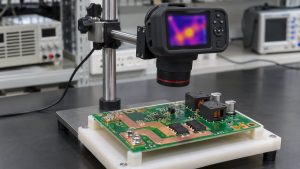
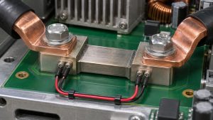
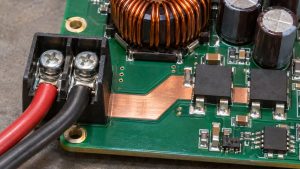
PCB busbar joint resistance is meaningful only when the measurement boundary is defined. A four-wire meter can remove most lead-voltage error, but it cannot decide which copper, solder, fastener or parallel path belongs in the result. Before accepting a joint, specify the sense locations, test current, temperature and circuit isolation. Then compare like-for-like results rather than applying a universal micro-ohm limit.
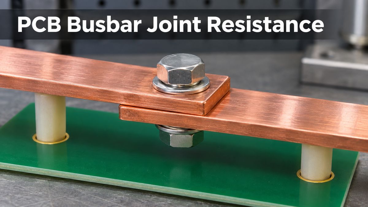
What Does a PCB Busbar Joint Resistance Test Measure?
The reading includes everything between the voltage-sense points that carries the measured current. It may include bulk conductor, a contact interface, solder and current-spreading regions. It is not automatically the interface resistance alone. A low result also does not prove adequate mechanical retention, insulation or long-term thermal performance.
This guide covers an isolated, unpowered assembly using a controlled DC resistance test. Live equipment and stored-energy systems require a separate approved safety procedure and appropriately rated instruments.
Why Can a Two-Wire Reading Be Misleading?
A two-wire instrument measures voltage across the device plus its test leads and contacts. Those additional resistances can overwhelm a low-resistance joint. Four-wire, or Kelvin, measurement drives current through one pair of connections and senses voltage through another high-impedance pair. Sense current is very small, reducing the effect of voltage drop along the sensing leads.
Four-wire sensing improves the electrical measurement; it does not remove errors from incorrect probe placement, an unstable contact or unintended current routes.
Detailed Test Parameters to Define Before Measurement
| Parameter | Record | Why it matters |
| Measurement boundary | Drawing coordinates or marked sense points | Defines the conductor length and interfaces included |
| Test current | Magnitude, direction and dwell | Controls signal level and possible self-heating |
| Temperature | Joint or assembly temperature and stabilization condition | Conductor resistance changes with temperature |
| Instrument | Range, resolution, uncertainty and calibration status | Display digits alone do not establish accuracy |
| Offset handling | Current reversal or approved compensation method | Thermoelectric voltage can bias small voltage readings |
| Circuit state | Isolated paths, connectors and stored-energy checks | Parallel conductors can reduce the apparent resistance |
Where Should Current and Sense Probes Be Placed?
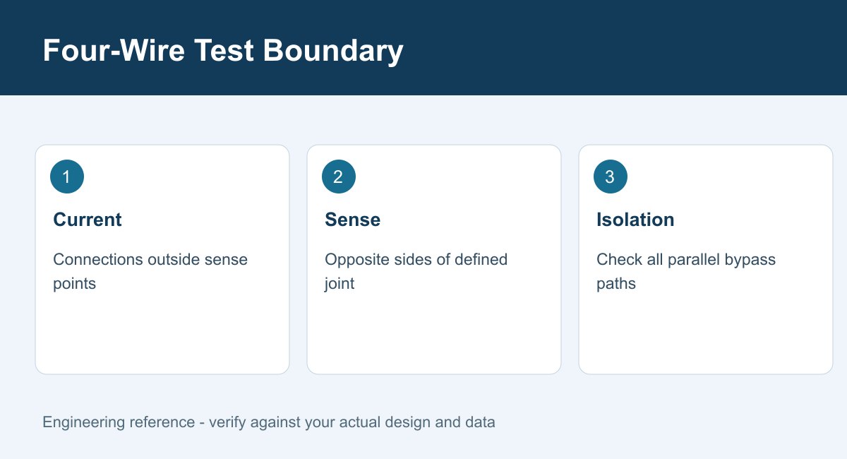
Put the current connections outside the intended sensing boundary. Locate the voltage probes on the controlled conductor surfaces on opposite sides of the joint. Use a drawing or fixture to reproduce those positions. Moving a sense probe farther along a copper bar adds conductor resistance; placing both probes on the same side of the interface may exclude the joint entirely.
Probe pressure, surface condition and current distribution near a connection can affect repeatability. Avoid claiming a single placement is correct for every busbar geometry: validate it for the actual assembly.
How Can Parallel PCB Copper Hide a Poor Joint?
A PCB plane, second busbar, cable, connected module or another joint can create a bypass around the test boundary. The meter then reports an equivalent network resistance rather than the intended joint. Disconnecting external power does not necessarily remove those paths.
Review the schematic and physical assembly together. Where isolation is impossible, document the network and use an approved model or another verification method. Never label a network reading as a standalone contact resistance without that qualification.
How Do Thermoelectric Offsets Affect Microvolt Signals?
Dissimilar-metal contacts at different temperatures can generate a small voltage independent of the test current. At low resistance, that voltage may be significant compared with the wanted signal. Keithley describes current reversal as one way to separate a stable offset from the resistive component.
For equal positive and negative current magnitudes, R = (V+ − V−)/(2I), provided the offset and resistance remain sufficiently stable between readings. Rapid temperature changes, settling errors or self-heating can invalidate that assumption. Use the instrument’s specified procedure rather than reversing an arbitrary power source manually.
How Should Test Current and Dwell Be Selected?
Choose current high enough for a resolvable voltage but compatible with the joint, PCB tracks, connectors and instrument compliance. Excess current or long dwell can heat the assembly and change the resistance being measured. A room-temperature resistance check is not the same as an operating-current temperature-rise test.
For illustration only, 10 A through 100 µΩ produces 1 mV and 0.01 W. These numbers explain signal scale; they are not recommended test settings or an acceptance threshold. Validate settings against the actual assembly and uncertainty target.
Kelvin DC Test vs Two-Wire Meter vs Thermal Test
| Method | Useful for | Limitation |
| Two-wire resistance | Continuity and higher-resistance checks | Lead/contact voltage drop can dominate a low-resistance joint |
| Four-wire DC resistance | Controlled low-resistance comparison | Requires defined boundaries, isolation and offset control |
| Operating-current thermal test | Temperature rise under defined cooling and loading | Depends on environment; does not isolate contact resistance by itself |
| AC impedance tester | Frequency-specific impedance measurements | Not interchangeable with DC joint resistance without validation |
What Acceptance Limit Is Defensible?
Derive limits from the electrical loss budget, allowable temperature rise, mechanical design and validation evidence. The simple relation P = I²R connects resistance to local loss, but it does not predict temperature without a thermal model or test. Consider current distribution and surrounding heat paths.
Record a qualified reference population under the same method, evaluate measurement uncertainty and define decision rules for readings near the limit. A limit from a power-distribution busway manual belongs to that manufacturer’s construction and procedure; it must not be copied directly onto a PCB-mounted joint.
Common Failure Patterns and Their Root Causes
| Observation | Check first | Do not assume |
| Unexpectedly low resistance | Parallel paths; both sense points on one side | That the joint is exceptionally good |
| Reading changes when probes move | Included conductor length and surface contact | That all variation comes from the joint |
| Drift during repeated readings | Thermal stabilization, offset and self-heating | That instrument resolution proves stability |
| High but repeatable result | Boundary, interface condition and assembly process | That tightening alone is an approved repair |
For bolted designs, use the drawing’s approved hardware and assembly process. For soldered or welded designs, investigate the applicable process evidence. Do not prescribe a universal torque, reflow profile or rework method across different constructions.
What Should the Repeatability Checklist Include?
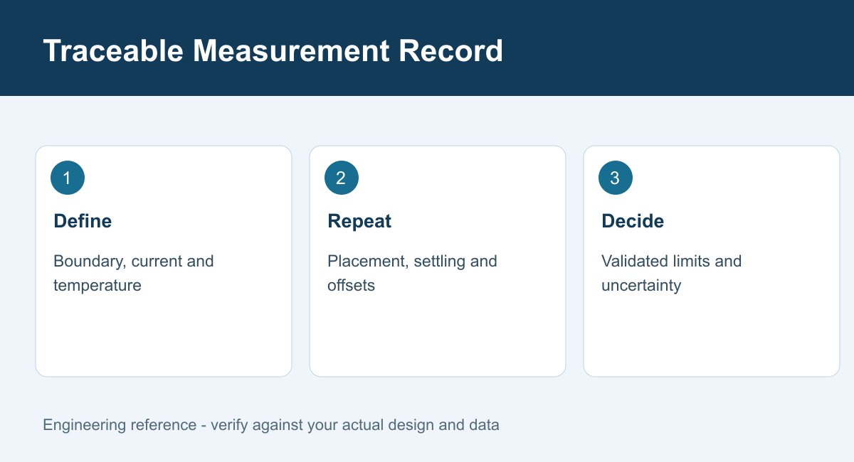
Confirm de-energization and discharge; identify current and sense points; check bypass isolation; verify instrument range and calibration; stabilize temperature; apply the validated current and settling time; repeat the measurement with controlled probe placement; record both the result and abnormal behavior. If reversal is used, retain enough information to detect an unstable offset.
What Should an Engineering or Supplier Review Receive?
Provide the busbar/PCB drawing, joint construction, intended current duty, thermal constraints, measurement boundary and acceptance method. Include the complete fixture and instrument conditions when comparing suppliers or production lots. A naked micro-ohm number is not a transferable specification.
For a special PCB manufacturing review, send the controlled design and test requirements to sales@bestpcbs.com. Test availability and production limits require project-specific confirmation.
FAQ
Can a normal multimeter measure a busbar joint accurately?
It may check continuity, but a two-wire reading can include more lead and probe resistance than the joint itself. Confirm range and uncertainty. For low-resistance acceptance, use a validated four-wire method with defined sense points and circuit isolation. Record the instrument model and selected range.
Are Kelvin clips sufficient to guarantee a correct result?
No. They provide separate current and voltage contacts, but placement, surface condition and circuit topology still matter. Confirm which contact is the voltage sense and which conductor sections lie between the two sense locations. Keep placement photographs or fixture references with the measurement record.
Can a battery tester replace a DC micro-ohmmeter?
Not automatically. Some testers measure AC impedance at a specified frequency rather than DC resistance. Different excitation and processing can produce different values. Use the instrument type required by the approved procedure or demonstrate equivalence for that assembly. Check the specified excitation frequency before comparing readings.
Why does the result drift after connecting the probes?
Possible causes include thermal EMF, unsettled contacts, changing temperature and test-current heating. Check the instrument’s settling requirements and repeat at controlled conditions. Drift is not enough by itself to identify a defective joint. Compare stabilized readings using the same current and sensing boundary.
Must PCB parallel paths be disconnected?
They must be removed, shown to be irrelevant or included explicitly in a validated measurement model. Otherwise, the result may describe a parallel network instead of the joint. An unpowered PCB can still contain conductive bypass paths. Document the isolation configuration with the measured value.
Is there a universal acceptable micro-ohm value?
No single number applies to every material, geometry and current duty. Establish a limit from the qualified design and thermal/electrical requirements, then account for the measurement method and uncertainty. Keep the probe boundary identical when comparing results. Avoid transferring limits between different joint constructions.
Can the busbar itself be used as a current shunt?
Only with suitable characterization and an approved design. Sense spacing, temperature coefficient, current distribution and calibration affect accuracy. A busbar selected for low loss is not automatically a precision shunt, even if its voltage drop can be measured. Separate current-monitoring accuracy requirements from joint-acceptance requirements.
Does passing resistance testing prove the joint is reliable?
No. It verifies one characteristic under one condition. Mechanical retention, insulation, thermal cycling, corrosion and operating temperature may need separate qualification. The required tests depend on the actual product and application, not the resistance reading alone. Keep qualification evidence separate from routine production measurements.
References
- Seaward/Cropico: low-resistance measurement and test-current selection
- Keithley Low Level Measurements Handbook
- Tektronix: low-voltage measurement techniques
- EAE KX manual: example of construction-specific busbar test requirements
Technical guidance is for engineering planning. Use qualified personnel, approved procedures and the actual instrument manual for testing.