The selective soldering process creates through-hole solder joints only at programmed locations on a PCB assembly. It is commonly used after SMT reflow when connectors, relays, transformers, terminals, switches, or other plated through-hole components still need to be soldered without exposing the entire underside of the board to a full solder wave.
Its advantage is control, but localized soldering does not automatically guarantee good joints. Flux placement, preheat, nozzle condition, solder contact, travel direction, withdrawal, PCB thermal mass, and inspection must work as one connected process. A setting that produces complete barrel fill on a plane-connected power pin may overheat a nearby low-mass joint. A nozzle path that works on an open connector row may bridge pins when an adjacent component changes the solder flow.
This guide explains how each stage works, which variables change the result, and how a stable selective soldering process turns mixed SMT and through-hole assemblies into repeatable production builds.
What Is the Selective Soldering Process?
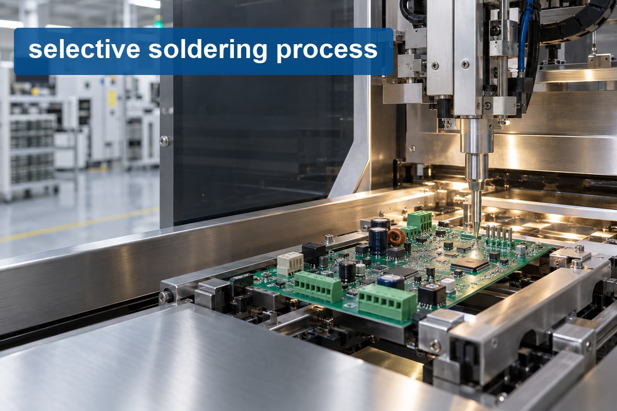
Selective soldering is an automated through-hole assembly process that delivers flux, heat, and molten solder to chosen joints instead of treating the entire PCB underside. A programmed system moves either the PCB or a small solder nozzle so that the solder fountain reaches the required pins while avoiding nearby areas.
The method is especially useful after one or both PCB sides have already passed through SMT reflow. Bottom-side resistors, capacitors, ICs, or other packages may sit close to the remaining through-hole pins. Full wave soldering could require a protective pallet or expose too much of the assembly to heat, while extensive hand soldering may add operator variation. Selective soldering in PCB assembly gives the assembler a repeatable route to the remaining joints when the layout provides sufficient access.
The process is not simply a smaller version of wave soldering. Each target receives its own controlled flux pattern and thermal history. The machine program must account for connector geometry, pin spacing, component mass, copper distribution, board thickness, solder alloy, surface finish, and the location of nearby components.
Selective Soldering Process Steps from Fluxing to Inspection
A production cycle normally follows five connected stages:
- Flux application: Flux is deposited only where the selected through-hole joints need it.
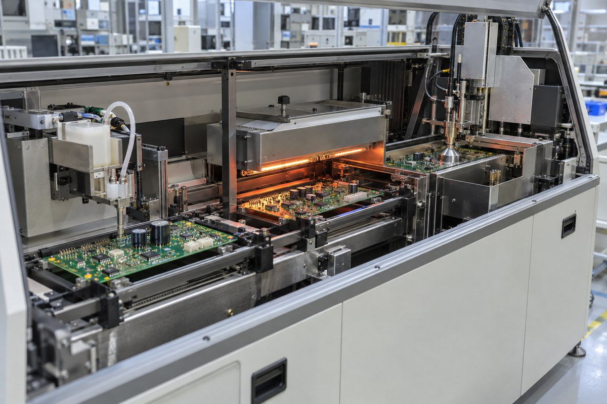
- Preheating: The PCB and component leads are brought to a suitable temperature so that the flux activates and the joint can accept solder.
- Localized soldering: A nozzle creates a stable mini-wave and follows the programmed path beneath the required pins.
- Cooling: The solder solidifies while the component and PCB remain stable.
- Inspection: The finished joints are checked for wetting, barrel fill, bridging, solder balls, damage, and other agreed acceptance criteria.
These stages cannot be tuned independently. Too much flux may spread beyond the intended area or leave active residue when preheat is insufficient. Weak preheat may force a longer solder-contact time, which can increase copper dissolution and thermal exposure. An unstable solder fountain can make a correct travel path produce inconsistent results.
For this reason, the first article should use the actual PCB, components, alloy, flux, nozzle, and production program. Once the joint results are approved, the program and material combination should remain under revision control.
How Flux Application and Preheating Prepare the PCB
Flux prepares the metal surfaces for wetting. It removes light oxides from the PCB finish and component leads, then helps molten solder spread into the plated hole. Selective equipment usually applies a controlled drop, jet, or spray pattern around the target area rather than coating the complete underside.
The deposit must reach the joint without flooding nearby components. Too little flux can cause non-wetting or incomplete barrel fill. Too much flux can splash, spread under low-clearance components, create solder balls, or leave residues that have not received enough heat to become benign. Flux chemistry must also match the alloy, board finish, cleaning plan, and product reliability requirements.
Preheat then activates the flux and reduces the temperature difference between the assembly and the molten solder. This is especially important for thick PCBs, heavy-copper constructions, large connector pins, and pins tied to power or ground planes. These structures draw heat away from the barrel. Without enough preheat, solder may wet the bottom pad but fail to rise adequately through the hole.
More heat is not always the answer. Excessive preheat can exhaust the useful flux activity before solder contact, stress temperature-sensitive parts, warp the PCB, or reduce the margin for nearby low-mass joints. A stable profile prepares the most demanding joints without overheating the rest of the assembly.
How the Solder Nozzle Forms Through-Hole Joints
The nozzle pumps molten solder into a small, continuously flowing fountain. The PCB or nozzle moves until the selected pins enter the controlled solder wave. Heat transfers through the leads, pads, and plated barrels; activated flux supports wetting; and capillary action helps solder rise through the hole.
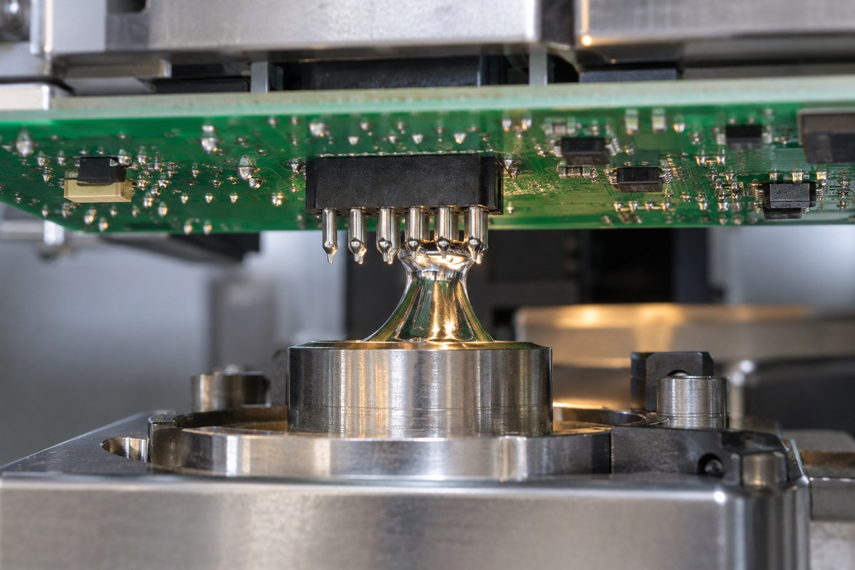
Nozzle diameter and shape must suit the accessible space and joint group. A larger nozzle can transfer more heat and process a row efficiently, but it requires more clearance. A smaller nozzle can reach isolated pins close to bottom-side SMDs, although its narrower thermal capacity may require a different speed or contact time.
Movement is part of joint formation. Approach direction, immersion depth, travel speed, dwell time, solder-flow height, and withdrawal angle affect how solder enters and leaves the joint. If the nozzle pauses too long, the PCB receives unnecessary heat. If withdrawal is poorly controlled, solder may remain between adjacent pins and create a bridge or icicle.
The nozzle also needs a clean and stable surface. Oxide buildup, contamination, uneven solder flow, or incorrect pump behavior can change the fountain even when the program remains unchanged. Routine nozzle maintenance and process checks therefore protect repeatability as directly as the stored motion program.
Which Parameters Control Selective Soldering Results?
The result comes from the combined thermal, chemical, mechanical, and geometric conditions at each joint. The most influential parameters include:
| Control | If it is too low or too short | If it is too high or too long |
|---|---|---|
| Flux deposit | Non-wetting or poor fill | Residue, splashing, or solder balls |
| Preheat | Inactive flux and cold barrels | Flux exhaustion, warpage, or component stress |
| Solder contact | Incomplete wetting or fill | Excess heat and copper dissolution risk |
| Travel speed | Insufficient heat transfer | Bridging or prolonged exposure |
| Solder-wave height | Unstable contact | Flooding or contact with nearby areas |
Board construction determines how those settings behave. Finished hole size, lead diameter, copper weight, plane connections, thermal reliefs, PCB thickness, surface finish, and component mass can make two visually similar pins need different thermal treatment.
The correct process window therefore comes from the actual assembly, not a universal temperature or speed copied from another job. When one pin is difficult, the team should identify whether the restriction comes from solderability, flux delivery, hole fit, thermal mass, nozzle access, or motion before changing the complete profile.
Selective Soldering Defects and Their Process Causes
Selective soldering defects are usually the visible result of an earlier process condition. Effective correction starts by tracing the defect back to fluxing, preheat, geometry, solder contact, movement, materials, or handling.
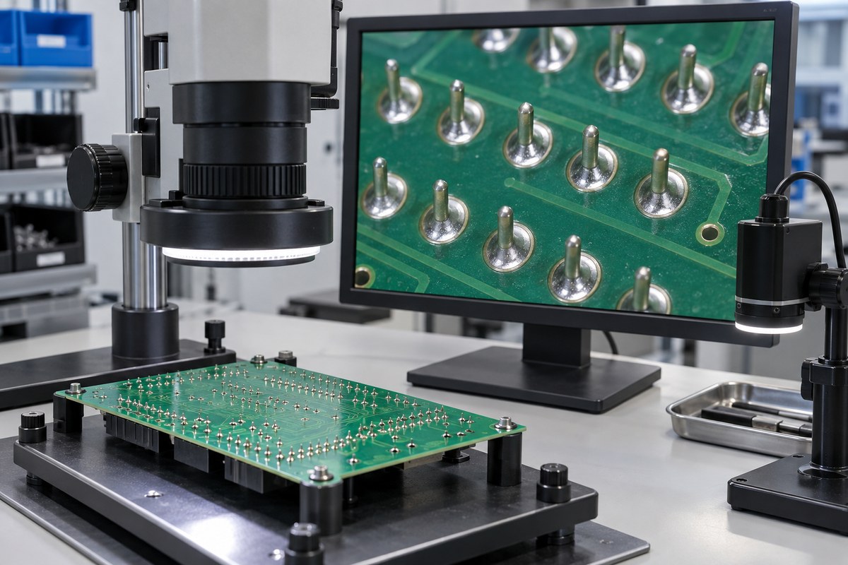
| Defect | Likely process causes | Practical investigation |
|---|---|---|
| Bridging | Excess contact, tight pitch, poor withdrawal, unstable flow | Check path, speed, nozzle, lead length, and mask geometry |
| Poor barrel fill | Low preheat, high thermal mass, weak wetting, unsuitable hole fit | Compare difficult pins with ordinary pins and review the thermal path |
| Non-wetting | Oxidized finish or leads, insufficient flux, contamination | Check storage, solderability, flux delivery, and surface condition |
| Solder balls | Excess flux, splashing, moisture, inadequate preheat | Review deposit volume, drying, material condition, and nozzle stability |
| Icicles | Slow or unstable withdrawal, excess solder contact | Review exit direction, travel speed, wave height, and lead protrusion |
| Pad or barrel damage | Excessive heat or repeated touch-up | Review contact time, solder temperature, rework history, and PCB condition |
Increasing solder temperature can appear to improve fill, but it can also accelerate copper dissolution, shorten the usable flux window, and increase thermal stress. Likewise, adding more flux may temporarily improve wetting while creating residue or reliability concerns elsewhere.
A useful defect review compares the failed joint with a successful joint on the same assembly. Differences in plane connection, pin mass, hole fit, local clearance, nozzle direction, or flux coverage often reveal the actual cause faster than changing several machine settings at once.
Selective Soldering vs Wave Soldering Process Differences
Both methods solder plated through-hole components with molten solder, but they create very different exposure and production conditions.
| Process factor | Selective soldering | Wave soldering |
|---|---|---|
| Solder contact | Programmed joints or groups | Most of the PCB underside |
| Typical fit | Mixed SMT/THT assemblies | THT-heavy, wave-compatible layouts |
| Main setup | Flux pattern, nozzle, path, and local profile | Conveyor profile, full wave, pallet or masking |
| Cycle behavior | Time grows with the programmed path | Many accessible joints solder at once |
| Main limitation | Nozzle access and local cycle time | Broad heat exposure and component protection |
Selective soldering is often preferable when bottom-side SMDs sit near a limited number of THT locations, when a connector needs more consistency than repeated hand soldering, or when board variants change the required joint locations. Wave soldering can remain more efficient when the underside is designed for broad solder exposure and many through-hole joints must be processed in one pass.
The choice should reflect the actual board. A selective process may avoid a dedicated wave pallet and reduce touch-up, yet its programmed cycle may be slower. Wave soldering may offer higher throughput, but masking, pallet cost, heat exposure, and rework can change the total production result.
Selective Soldering Process for Mixed SMT and Through-Hole Assemblies
Consider a double-sided SMT assembly that receives a multi-pin connector, a relay, and a plane-connected power terminal after reflow. Bottom-side passives sit close to the connector pins, while the power terminal draws heat into a large copper area.
The connector row may suit a shaped nozzle that solders several pins along one controlled path. Nearby SMDs determine the available nozzle diameter and travel direction. The power terminal may need stronger preheat or a separate dwell condition because its copper connection removes heat faster than the connector pins. The relay body and leads must remain clear of the nozzle approach and withdrawal path.
This assembly should not be validated by looking only at the easiest connector pins. Inspection must include the plane-connected terminal, the connector ends where bridging may occur, and any joint close to a bottom-side package. If those locations meet the agreed criteria without excessive touch-up, the process has demonstrated control across the actual thermal and geometric range of the PCB.
If the nozzle cannot reach a pin, the solution may require a layout adjustment, different PCB assembly fixtures or panel support, another nozzle, approved hand soldering for that location, or a different overall soldering method. Programming cannot recover physical access that the assembled board does not provide.
How EBest Circuit Controls the Selective Soldering Process
For a released PCBA project, EBest Circuit reviews the board data, BOM, assembly drawing, component geometry, panel method, soldering requirements, and inspection criteria before production. This helps identify blocked joints, high-thermal-mass pins, tight connector spacing, special alloy or cleaning requirements, and locations that may need separate process treatment.
PCBA process control focuses on the items that determine repeatability:
- matching the PCB and assembly revisions to the approved production package;
- confirming component orientation, insertion, lead condition, and accessibility;
- setting flux, preheat, nozzle, path, and solder-contact conditions for the actual board;
- checking ordinary joints and thermally demanding joints during the first article;
- recording the approved process and controlling later changes;
- inspecting finished joints against the customer’s specified workmanship criteria;
- completing agreed electrical testing, traceability, and production records.
The customer remains responsible for the released circuit design, component approval, regulatory requirements, and final product validation. EBest Circuit’s role is to turn the approved PCB and PCBA data into a controlled manufacturing process and to resolve manufacturability questions before they become repeated soldering defects.
For a selective-soldering review, send the Gerber files, drill data, BOM, placement file, assembly drawing, component details, quantities, solder alloy, cleaning requirements, and inspection or testing requirements to sales@bestpcbs.com.
FAQs About the Selective Soldering Process
Is selective soldering used before or after SMT reflow?
It is commonly used after SMT reflow. The SMT components are soldered first, and the remaining through-hole connectors, terminals, relays, or other components are then processed at selected locations.
Is selective soldering the same as selective wave soldering?
Selective wave soldering is the common automated method that uses a localized mini-wave or nozzle. “Selective soldering” is the broader term and can include other localized soldering methods.
Can every through-hole component be selectively soldered?
No. The nozzle needs physical access, suitable clearance, a stable thermal path, and a workable soldering surface. Blocked pins or incompatible component geometry may require a layout change or another approved process.
What usually causes poor hole fill in selective soldering?
Common causes include insufficient preheat, high copper mass, unsuitable hole-to-lead fit, weak solderability, inadequate flux activation, or too little solder-contact time. The cause should be identified before raising temperature or dwell time.
Does selective soldering eliminate manual soldering?
It can greatly reduce manual work on accessible, repeatable joint groups. Very low-volume builds, blocked joints, wires, or exceptional component locations may still require a controlled and approved manual operation.
The best selective soldering process is not the one with the highest temperature or the longest contact time. It is the process that delivers enough flux and heat to every required joint, avoids unnecessary exposure elsewhere, and produces repeatable evidence that the complete assembly meets its approved acceptance criteria. Send your PCB files, BOM, quantities, and requirements to sales@bestpcbs.com for a PCBA manufacturing review.
You may also like





Tags: selective soldering process, selective wave soldering, through-hole pcb assembly